Minimal resonator loss for circuit quantum electrodynamics
Abstract
Single photon level quality factors of are shown in NbTiN superconducting resonators at millikelvin temperatures. This result originates from the intrinsic low dielectric loss of NbTiN, as demonstrated by comparison with Ta, and by removing unnecessary parts of the dielectric substrate.
In circuit quantum electrodynamics quantum information processing is done by coupling the qubit state to a single photon bound to a superconducting resonator wallraff . The lifetime of a single photon with frequency is defined by: wang , therefore a high resonator quality factor () is needed to maximize the lifetime. Presently used resonators, made from Nb or Al, have quality factors on the order of to wang ; oconnell ; palacios ; macha ; lindstrom . In contrast, superconducting resonators for astronomical photon detection day have shown quality factors in excess of a million. However, these quality factors are measured in the many-photon regime. One would like to maintain these high values down to the single photon level. Therefore, we study the unloaded quality factor of NbTiN and, for comparison, Ta quarterwave resonators down to the single photon level. NbTiN has been shown to follow Mattis-Bardeen theory more closely than Nb, Al or Ta, indicating it has a minimal dielectric layer compared to the latter materials barendsapl . We find that in the single photon regime the quality factor of NbTiN resonators is so high that the loss is largely due to the exposed substrate surface. In contrast, for Ta resonators the quality factor is limited by the metal surface. We show that a further reduction of the loss in NbTiN resonators is achieved by removing the substrate from the regions with a high electric field density. This increases the quality factor to half a million for resonators with a central line width of 6 m, three times higher than recently reported for Re wang .
We use NbTiN quarterwave coplanar waveguide resonators which are capacitively coupled to a feedline day ; barendsapl . This allows extracting the unloaded quality factor from the feedline transmission. For comparison we have also made Ta resonators. The NbTiN films, 300 and 50 nm thick, are DC sputter deposited on a hydrogen passivated high resistivity ( kcm) -oriented Si wafer. The NbTi target used contains 70 at. % Nb and 30 at. % Ti. Patterning is done by reactive ion etching in an SF6/O2 plasma. For the 300 nm thick film the critical temperature is K, the low temperature resistivity is cm and residual resistance ratio . For the 50 nm thick film: K, cm and . The 150 nm thick Ta film ( K, cm and ) is sputtered on a similar wafer and patterned in a CF4/O2 plasma. The devices are cooled to 310 mK using a He-3 sorption cooler, with the sample space magnetically shielded by a superconducting shield, and down to 60 mK using an adiabatic demagnetization refrigerator with the sample space shielded by an outer cryoperm and inner superconducting shield barendsthesis . Measurements have been done using a vector network analyzer which is locked to a frequency standard. A microwave isolator is placed in front of the low noise amplifier.
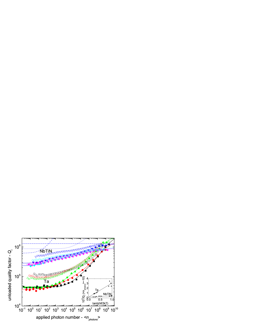
The unloaded quality factor of NbTiN and Ta resonators is plotted versus applied photon number numberofphotons in the resonator in Fig. 1. The resonators have resonance frequencies in the 3-6 GHz range, a central line width of m and a gap width of m. Bath temperatures are 60 mK and 310 mK. In the many-photon regime, quality factors between and are observed for both materials. In addition, in this regime the 60 mK and 310 mK data overlap. With decreasing applied photon number the quality factors decrease. For NbTiN resonators, a weak intensity dependence is observed and quality factors decrease to at 60 mK in the single photon regime. On the other hand, Ta quality factors degrade quickly, decreasing to . Interestingly, an inflection point is visible in the NbTiN data around , whereas Ta data show a plateau at low intensities. Additionally, at low intensities a temperature and frequency dependence develops for both materials. At 310 mK (open symbols) the quality factors are increased, for resonators with lower frequencies the increase is larger.
Previously, we have shown that NbTiN resonators contain fewer dipole two-level systems (TLS) than Ta, by measurements of the resonator frequency temperature dependence barendsapl . Dipole TLS are configurational defects with dipole moment which reside in amorphous dielectrics phillips , such as native oxides. Dielectric loss at low temperatures () arises from resonant absorption: phillips ; martinis . The factor reflects the thermal population difference between the lower and upper level. With increasing intensity TLS are excited, lowering the loss. The saturation field is controlled by the dipole moment and relaxation times and .
The microwave loss of our resonators in the single photon regime scales with , see the inset of Fig. 1, consistent with resonant absorption from TLS. Moreover, different resonators made from the same material follow the same trend, indicating that the loss is very comparable over the whole chip. In addition, the slope for Ta is steeper than for NbTiN, consistent with a larger TLS density for Ta, compared to NbTiN resonators.
In order to identify the location of these TLS and quantify the influence of their saturation on the quality factor, we calculate the effect of a hypothetical thin dielectric layer with thickness containing TLS. Dielectric loss in a quarterwave resonator due to a distribution of dipole TLS is given by wang ; gao
| (1) |
with the standing wave voltage inside the resonator, its length and the capacitance per unit length. The dielectric loss of the layer is , with the TLS density of states and and the volume and relative permittivity of the dielectric layer hosting the TLS.
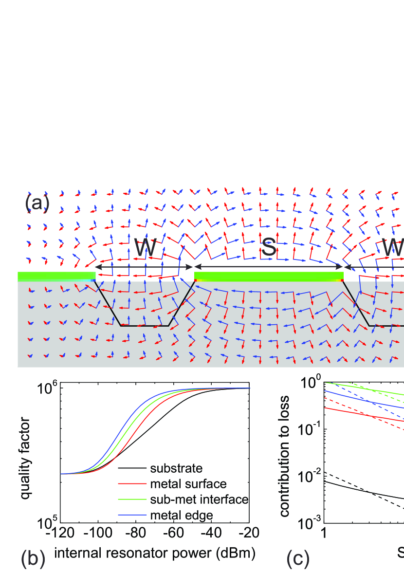
The electric fields for our resonator geometry are calculated by using the potential matrix to find the charge density : wang ; finiteelements . The substrate is included using the method of partial image charges. The potential matrix elements are given by for , and , with the location of the -th element, the location of the -th element mirrored in the plane of the substrate surface, its radius, and the relative permittivity of the substrate. The electric fields and magnetic fields are shown in Fig. 2a.
We place this hypothetical layer on either the exposed substrate surface, top metal surface, etched metal edges or at the substrate-metal interface. Interestingly, when the dielectric layer is placed on any of the metal surfaces, its contribution to the loss is two orders of magnitude larger than when placed on the exposed substrate surface (Fig. 2c). This can be attributed to the high electric fields near the metal surfaces. In addition, a dielectric placed in the vicinity of the metal leads to a much stronger power dependence than when the dielectric layer is located on the exposed substrate surface (Fig. 2b). We make use of this to distinguish between surfaces. Furthermore, the quality factor increases with increasing central line width, irrespective of the location of the dielectric.
In Fig. 1, we show that the power dependence of the quality factor arises from the superposition of loss (solid lines) from TLS (Eq. 1) located at the metal surfaces (dashed line) as well as at the exposed substrate surface (dotted line). Interestingly, for NbTiN resonators the exposed substrate, together with the metal surfaces, is a significant contributor to the microwave loss. This superposition of loss closely describes the observed point of inflection at as well.
| material | () | (1/nm) | (kV/m) |
|---|---|---|---|
| NbTiN | 0.9-1.3 | 330-450 | 0.05 |
| Ta | 1.7-3 | 70-90 | 0.1-2 |
| Si (NbTiN) | 13-16 | 5 | |
| Si (Ta) | 1.1-1.9 | 2 |
The saturation fields of NbTiN are on the order of 50 V/m, see Table 1, similar to values for Re and Al wang . For Ta we find a large spread in the saturation fields. The dielectric loss of NbTiN is clearly smaller than that of Ta. The substrate surface values are consistent with SiOx. The saturation field is kV/m; comparable to measurements on vitreous silica: D, s and ns schickfus . Moreover, a value of kV/m has been reported for SiO2 also by Martinis et al. martinis . The quality factor of the Si surface layer, assuming nm and , lies around 15-200, which is on the order of the value of reported for SiO2 martinis . At high intensity the quality factors are temperature independent, suggesting loss other than due to TLS. We include an intensity-independent fitting term to account for this loss. We suspect that we reach the level of the intrinsic loss of the superconductor. For Ta, relaxation times saturate for barendsPRL , suggesting that the quasiparticle density becomes temperature independent. At we estimate based on Mattis-Bardeen, on the order of values found for .
The data in Fig. 1 and the analysis provide a clear guide towards improving the quality factor. We have shown that Ta suffers from significant microwave loss due to dipole TLS in its metal surface, i.e. its native oxide. We believe that the presence of a native oxide is the reason why resonators made of Nb, Ta, Al, or deposited on top of SiO2, consistently show low quality factors in the single photon regime wang ; oconnell ; palacios ; macha ; lindstrom . In this respect NbTiN is different, because the metal atoms are bound to nitrogen. Moreover, resonators with m and m have quality factors around , nearly a doubling compared to Re on Si resonators which have quality factors around (loaded, with ) and are wider ( m and m) wang . Nevertheless, the NbTiN resonator quality factor is significantly limited by the exposed and oxidized Si surface. Therefore NbTiN has a clean surface compared to Si, as the metal surface influences the loss much stronger than the exposed substrate (Fig. 2c). Consequently, removal of the Si from the gaps will increase the quality factor.
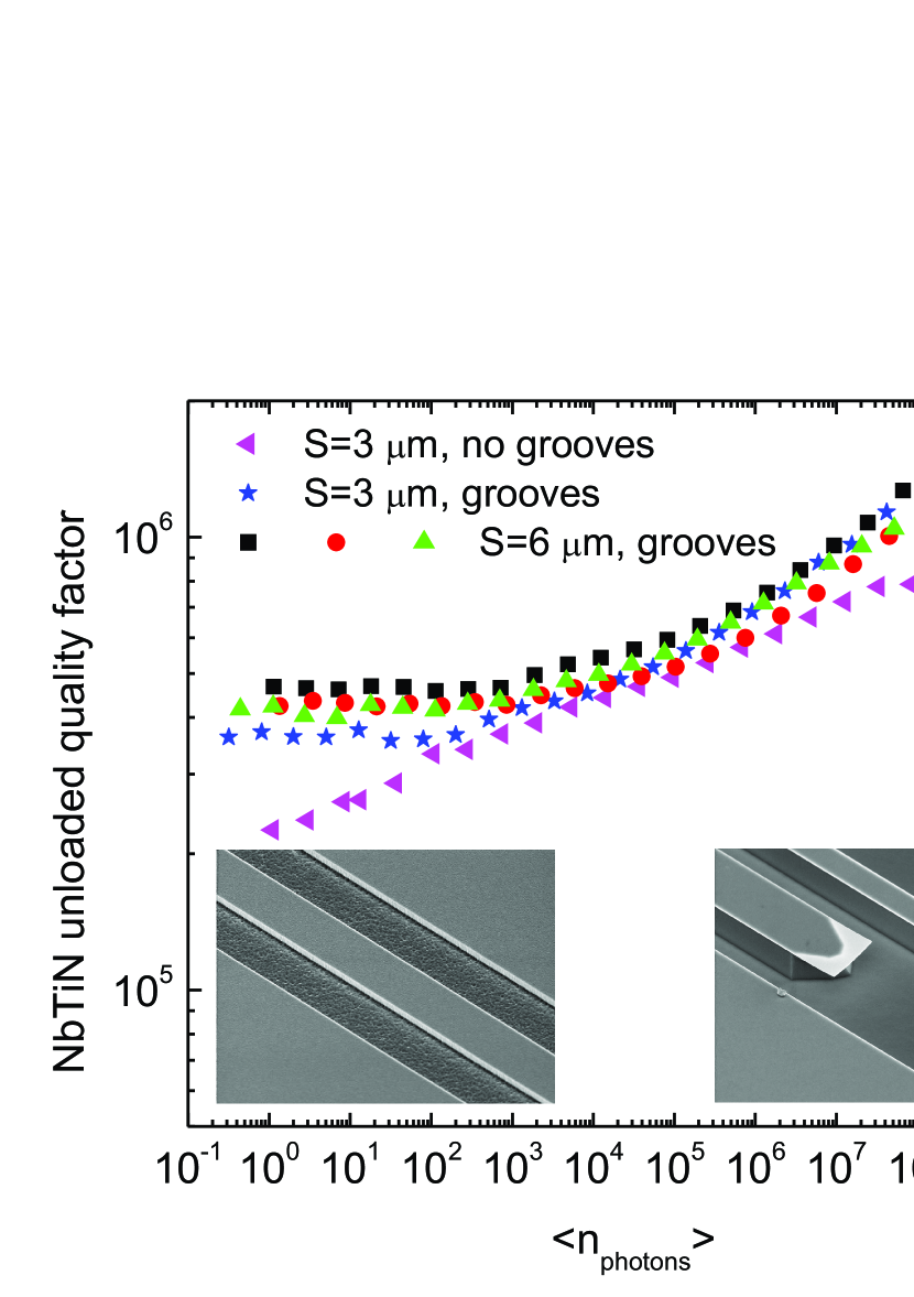
With NbTiN shown to be a superior superconductor, we have redesigned our resonators to have fewer dielectrics. We have made 50 nm thick NbTiN resonators, fully straight, which are aligned along the axis of the -oriented HF-cleaned Si wafer. Using KOH wet etching, grooves of 0.9 m deep are etched in the gaps along the full length of the resonators, see the inset of Fig. 3; this removes the substrate surface from the region with the highest electric field density (black lines in Fig. 2a).
The NbTiN resonators with grooves etched in the gaps have significantly higher quality factors, see Fig. 3. In the single photon regime, the quality factor has improved from a value of for the standard design to an intensity-independent plateau value of for the etched resonators, for m and m. Moreover, this increase is a clear indication that the Si surface was the limiting factor also for another reason: the decrease of dielectric has lead to a decrease in the capacitance in Eq. 1. Therefore, if the metal surfaces would dominate the losses, the quality factors would decrease. The intensity-independent plateau points towards a single surface dominating loss. With the Si removed, the loss at the single photon level is dominated by the metal surfaces. Determining which surface is complicated by the similarity in dependence on intensity and width (Fig. 2). In the many-photon regime the loss is more due to the exposed substrate surface, indicated by the higher quality factors for etched resonators and the high saturation field values. Finally, when increasing the width to m and m, the quality factor improves to around . This 30 % increase is consistent with our calculation (Fig. 2b) and shows that further increases can be obtained by widening the resonator.
With quality factors as high as , we estimate single photon lifetimes of 18 s at 4.2 GHz, one order of magnitude longer than decoherence times measured for superconducting qubits bertet ; houck . These long lifetimes make superconducting resonators, as shown in Fig. 3, appealing building blocks for a quantum processor, as they can be used as quantum memory elements leek and for a quantum bus for long-range qubit-qubit coupling sillanpaa ; majer .
To conclude, we have found NbTiN resonators to have a higher quality factor in the single photon regime than any of the previously studied superconductors, indicating it has a minimal lossy dielectric layer. The losses arise largely due to a surface distribution of two-level systems on the exposed Si substrate. By removing the substrate from the region with highest electric fields the quality factor is increased further, showing that using NbTiN resonators and removing dielectrics is a straightforward route to high quality factors in the single photon regime.
Acknowledgements.
The authors thank J. M. Martinis and P. Forn-Díaz for stimulating discussions. The work was supported by the Pieter Langerhuizen Lambertuszoon funds of the Royal Holland Society of Sciences and Humanities and by the EU NanoSciERA project “Nanofridge”.References
- (1) A. Wallraff, D. I. Schuster, A. Blais, L. Frunzio, R. S. Huang, J. Majer, S. Kumar, S. M. Girvin, and R. J. Schoelkopf, Nature 431, 162 (2004).
- (2) H. Wang, M. Hofheinz, J. Wenner, M. Ansmann, R. C. Bialczak, M. Lenander, E. Lucero, M. Neeley, A. D. O’Connell, D. Sank, M. Weides, A. N. Cleland, and J. M. Martinis, Appl. Phys. Lett. 95, 233508 (2009).
- (3) A. D. O’Connell, M. Ansmann, R. C. Bialczak, M. Hofheinz, N. Katz, E. Lucero, C. McKenney, M. Neeley, H. Wang, E. M. Weig, A. N. Cleland, and J. M. Martinis, Appl. Phys. Lett. 92, 112903 (2008).
- (4) P. Macha, S. H. W. van der Ploeg, G. Oelsner, E. Il ichev, H.-G. Meyer, S. Wünsch, and M. Siegel, Appl. Phys. Lett. 96, 062503 (2010).
- (5) T. Lindström, J. E. Healey, M. S. Colclough, C. M. Muirhead, and A. Ya. Tzalenchuk, Phys. Rev. B 80, 132501 (2009).
- (6) A. Palacios-Laloy, F. Nguyen, F. Mallet, P. Bertet, D. Vion, and D. Esteve, J. Low Temp. Phys. 151, 1034 (2008).
- (7) P. K. Day, H. G. LeDuc, B. A. Mazin, A. Vayonakis, and J. Zmuidzinas, Nature 425, 817 (2003).
- (8) R. Barends, H. L. Hortensius, T. Zijlstra, J. J. A. Baselmans, S. J. C. Yates, J. R. Gao, and T. M. Klapwijk, Appl. Phys. Lett. 92, 223502 (2008).
- (9) R. Barends, Ph. D. thesis, Delft University of Technology, 2009.
- (10) Applied number of photons: , with the standing wave voltage, the internal resonator power barendsthesis and the waveguide impedance.
- (11) W. A. Phillips, Rep. Prog. Phys. 50, 1657 (1987).
- (12) J. M. Martinis, K. B. Cooper, R. McDermott, M. Steffen, M. Ansmann, K. D. Osborn, K. Cicak, S. Oh, D. P. Pappas, R. W. Simmonds, and C. C. Yu, Phys. Rev. Lett. 95, 210503 (2005).
- (13) J. Gao, M. Daal, A. Vayonakis, S. Kumar, J. Zmuidzinas, B. Sadoulet, B. A. Mazin, P. K. Day, and H. G. LeDuc, Appl. Phys. Lett. 92, 152505 (2008).
- (14) P. P. Silvester and R. L. Ferrari, Finite elements for electrical engineers, 2nd edition (Cambridge University Press, 1989).
- (15) M. von Schickfus and S. Hunklinger, Phys. Lett. 64A, 144 (1977).
- (16) R. Barends, J. J. A. Baselmans, S. J. C. Yates, J. R. Gao, J. N. Hovenier, and T. M. Klapwijk, Phys. Rev. Lett. 100, 257002 (2008).
- (17) P. Bertet, I. Chiorescu, G. Burkard, K. Semba, C. J. P. M. Harmans, D. P. DiVincenzo, and J. E. Mooij, Phys. Rev. Lett. 95, 257002 (2005).
- (18) A. A. Houck, J. A. Schreier, B. R. Johnson, J. M. Chow, J. Koch, J. M. Gambetta, D. I. Schuster, L. Frunzio, M. H. Devoret, S. M. Girvin, and R. J. Schoelkopf, Phys. Rev. Lett. 101, 080502 (2008).
- (19) P. J. Leek, M. Baur, J. M. Fink, R. Bianchetti, L. Steffen, S. Filipp, and A. Wallraff, Phys. Rev. Lett. 104, 100504 (2010).
- (20) M. A. Sillanpää, J. I. Park, and R. W. Simmonds, Nature 449, 438 (2007).
- (21) J. Majer, J. M. Chow, J. M. Gambetta, J. Koch, B. R. Johnson, J. A. Schreier, L. Frunzio, D. I. Schuster, A. A. Houck, A. Wallraff, A. Blais, M. H. Devoret, S. M. Girvin, and R. J. Schoelkopf, Nature 449, 443 (2007).