Highly sensitive, photon number resolving detectors mediated by phonons using -doped GaAs transistors
Abstract
We report a photon number resolving detector using two-dimensional electron gas (2DEG) based transistors. When the photon pulses impinge on the absorption region, the generated phonons dissipate ballistically in the 2DEG toward the trench isolated nanowire transistors near the surface. The phonon-electron interaction induces a positive conductance in the transistors, resulting in a current increase. With this principle, we obtain an internal quantum efficiency for this type of detector of up to 85%.
Highly sensitive photon detection is in demand for the implementation of quantum information processing1 and improved optical sensors 2. Recently, several photon number resolved (PNR) detectors have been demonstrated using superconducting nanowires 3, 4, quantum dot gated field-effect transistors 5, superconducting transition-edge sensors 6, 7, visible light photon counters 8, charge integration photon detectors 9, silicon photomultipliers 10 and avalanche photodiodes 11. Among them, there are two types of PNR detector. One assembles multiple pixels to increase detection area 10, 3 while the other only has a single detector element 4, 5, 11. In the first case, only the photon number can be counted and it is not possible to resolve which pixel detected the photons. In contrast, the single element detector gives the chance to resolve photon energy and photon number when the photons impinge on the absorber. In semiconductor-based optical detection, optical to electrical conversion is normally realized by optically generated carriers in semiconductors 12, 5, 11, 9. The generated carriers either change the device current directly or act as a gate through capacitive coupling. Because of the recombination of the carriers, the sensitivity of the photon detection is intrinsically limited, which restricts the use of such devices for high sensitivity applications. However, phonons are also created with optical excitation 13, and it is possible to use these optically generated phonons for photon detection.
When light with a photon energy larger than the band gap is absorbed by a semiconductor, charge carriers are generated with a certain kinetic energy. The excited electrons and holes then typically relax down to the conduction and valence band edges via phonon emission. If the excess energy is larger than the energy of one LO phonon, then LO phonons are emitted, rapidly decaying to acoustic phonons within several picoseconds 14; otherwise, only acoustic phonons are expected. When photon pulses impinge on an absorption region, the generated phonons dissipate ballistically in the first instance.
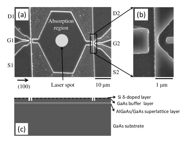
In this letter, we report a photon number resolving detector, which comprises an absorption region and two nanowire transistors, as shown in Figure 1 (a) and (b). When photons impinge on the absorption area, phonons are generated and then dissipated in a ballistic way towards the transistors aided by the phonon focussing effect. The phonons reflected by the superlattice buffer layer, and the back surface of the wafer, can be absorbed by electrons in the nanowires, increasing their conductance. The quantum efficiency of this type of photon detector can be up to 85%.
When the phonons propagate towards the trench-isolated nanowire transistors nearby (as shown in Figure 1 (a)), they can be absorbed by the transistors across the trench because of the reflection from the superlattice layer and the back surface of the wafer 15, 16. Hot phonons have been detected laterally using a 2DEG based nanowire transistor 17, 18. Here we focus on the optically-generated phonon assisted effect. In a two dimensional electron gas (2DEG) system, the transport properties depend largely on electron-electron and electron-phonon interactions. When the electron-electron interaction is much faster than the electron-phonon processes, phonon absorption will increase the electron energy, generally resulting in a conductivity change 19, 20. -doped GaAs has been demonstrated to be a good candidate of this type of system 21 because of the strong scattering by impurities. Recently, a positive phonon-conductivity has been demonstrated in a quasi-2D -doped GaAs based nanowire device, resulting in an increase (up to 40 S/square) in the drain current of the transistor 22. With this principle, we expect optically-generated phonons will induce a current increase, allowing photon detection.
A Si -doped GaAs wafer with a carrier concentration around cm-2, about 30 nm below the wafer surface, was used for these optical detection devices. A superlattice buffer layer around 200 nm was grown on the GaAs wafer to minimise defect propagation from the substrate into the active region. A buffer layer of GaAs was then deposited with a thickness of 1.5 m before the -doped layer growth. The device mesa was patterned using standard electron-beam lithography and reactive ion etching techniques. A layer of polymethylmethacrylate (PMMA) electron beam resist with a thickness around 700 nm was used as an etch mask during the etching of the isolation trenches. Ohmic contacts to the electrodes were formed by annealing a deposited Au:Ge:Ni alloy at . The depth of the mesa trench is about 1 m. A cross section through the device is illustrated in Figure 1 (c). Although the lithographic size of the wires is 100 nm, surface depletion means that the electrical width of the wire is much smaller, and can be controlled by the lateral gate electrode.
The device was mounted onto a cold-finger cryostat, and measured at a temperature of around 8.0 K. A DC bias from a low-noise voltage source in series with low-noise filters was applied to each drain lead and to the gates of both transistors. The gate voltages were optimized for sensitivity and visibility. The outputs of the source electrodes were fed into two low-noise current preamplifiers. A laser diode with emission wavelength at 808 nm was driven with a dc bias and a superimposed voltage pulse from a function generator. The frequency can be tuned from 0.01 Hz to 200 MHz. The power from the laser was carefully calibrated and attenuated using neutral density filters. Each neutral density filter was calibrated separately to obtain an accurate light intensity. The variation of the stability of the laser diode driver is around 0.5 % and the error of the photon number calibration is about 1%. The laser light after the attenuators was focused to the absorption area using a long working distance objective (100). The beam spot is about 5 m in diameter, as shown in Figure 1 (a). The reflection from the surface of the absorption area is about 27.6 2 %, which was calibrated using a beam splitter before the objective. This value corresponds well to the result (28.3 %) calculated by the Fresnel equation with a refractive index for GaAs of 3.3. The average photon number referred to in this paper is the photon number incident on the chip, excluding the reflection from the surface.
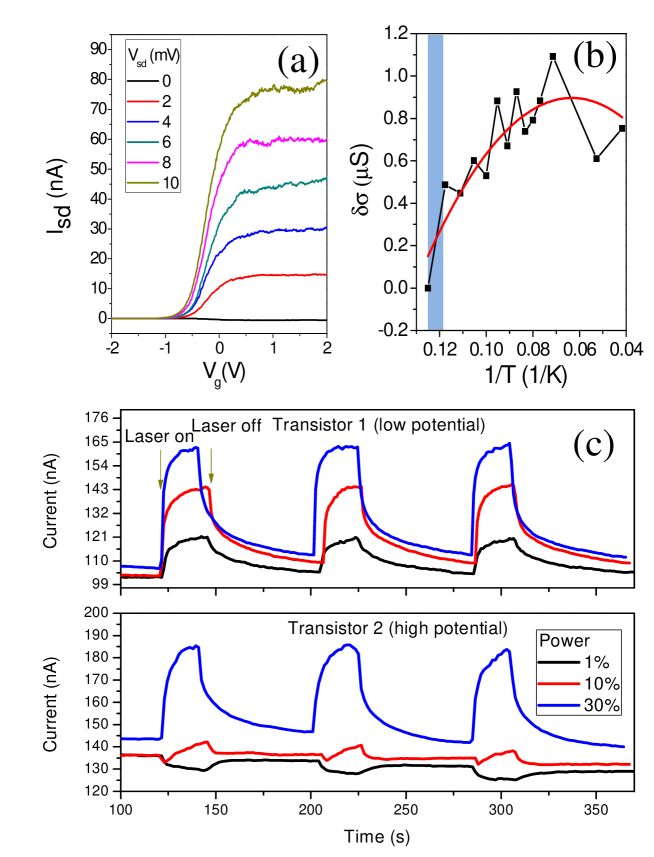
Figure 2 (a) shows the source-drain current of one of the transistors as a function of gate voltage at different drain voltages. A typical transistor characteristic can be observed and the drain current is saturated when the gate voltage is around 0.5 V. This transistor can be operated as a single electron transistor at 4.2 K or even in the optical cryostat at 8K, which means it is very sensitive to changes in local charge distribution to well below the single-electron level.
To demonstrate the phonon-induced conductance of the transistors, the temperature-dependent conductance of one transistor is plotted in Figure 2 (b). It can be seen that the conductance increases when the temperature increases from 8 to 14 K. This indicates the positive phonon-induced conductance (PIC) in the nanowire transistors. Assuming the time of electron-phonon interaction is much greater than the time of electron-electron collisions 19, it is possible to observe positive PIC when the length of a wire is longer than the elastic mean free path 23. This positive PIC is due to the increase of electron temperature under the absorption of phonon flux, which is given by 22
| (1) |
where , is the Boltzmann constant and is the temperature before heating. The solid line (red) shows the fitted results in Figure 2 (b). In this case, the electron temperature is same as the crystal temperature. It should be noted that for the weak light detection, especially for the photon number resolved detection in this work, the photon induced crystal temperature change can be neglected, being much less than 1 mK.
Further evidence for an optically generated phonon-induced positive current can be found by biasing the two transistors relative to one-another. The two transistors were floated and a bias voltage was applied between them. With this lateral field, the electron-hole pairs generated by optical pumping will be separated; electrons moving to one transistor and holes to the other. The top (bottom) panel in Fig. 2 (c) shows the optical response of the low (high) potential transistor. At the transistor with low (high) potential, holes (electrons) move towards it and act as a positive (negative) gate voltage, resulting in a current increase (decrease) at low optical power. For the transistor at high potential, the current decreases only at low optical power (1% of the laser power, the bottom trace). When the optical power is increased to 10%, the current decreases quickly due to the negative charge gating, then increases slowly, which we ascribe to the heating effect. With a power around 30%, no negative gate effect can be observed.
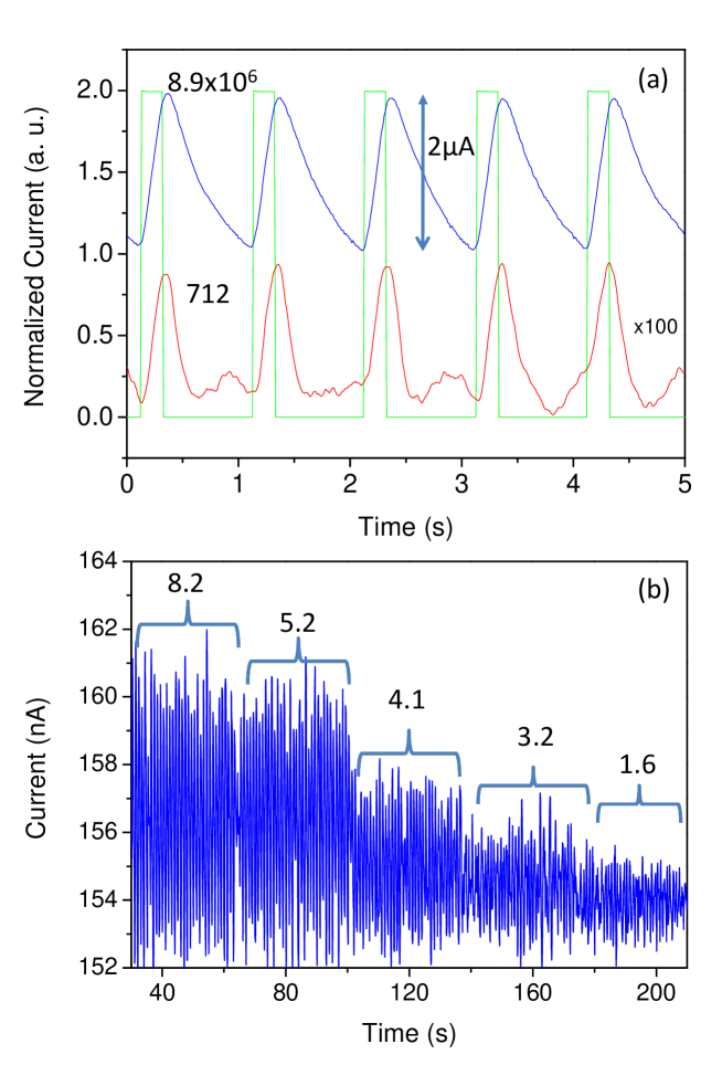
To perform single-shot measurements, the laser diode was modulated at 1 Hz, and the drain currents were measured by a voltage meter via low-noise current pre-amplifiers. Figure 3 (a) shows the single-shot measurements of photon induced current of one of the transistors with an average photon number () in each pulse of and 712, respectively. The current builds up within the optical pulse up to about 2 A and then decreases slowly. When decreases, the amplitude of the current peaks reduces. With at , the current continues to increase about 50 ms after the optical pulse is switched off, then decreases. This slower response, compared with the results in ref [22], is due to the low-pass filters in this measurement. It should be noted that the current did not drop to the equilibrium level at high optical power before the next pulse arrived, therefore the current increase does not linearly depend on the power. The responses of the two transistors are similar. The current change can be measured when the laser intensity was attenuated to a few photons per pulse. The real-time signal with () from 1.6 to 8.2 per pulse is shown in Figure 3 (b). We concentrate on low photon number detection here because the conductance does not always respond linearly with phonon number 22.
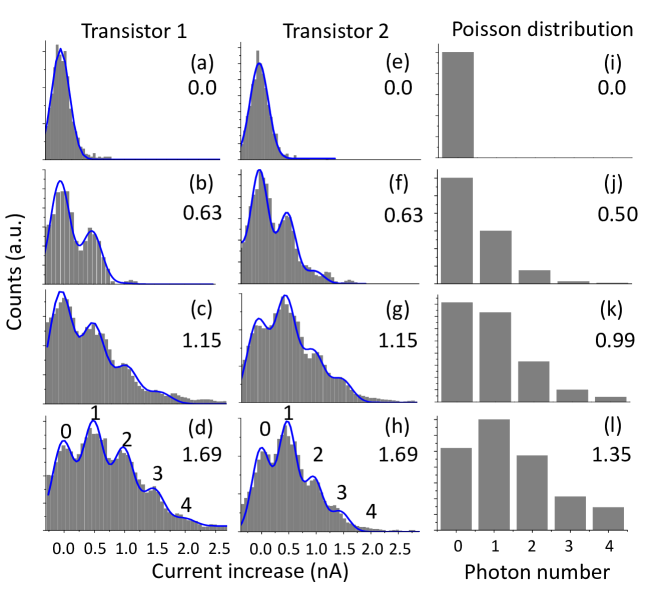
In order to confirm photon number resolution, histograms of the current change of the two transistors were constructed, as shown in Figure 4. Figure 4 (a)-(d) and (e)-(h) show the histograms of Transistor 1 and Transistor 2 respectively, with average photon number of 0, 0.63, 1.15, and 1.69. It can be seen that each number of photons can be well resolved. The solid blue line is the sum of a series of Gaussian functions with the same peak separation. The average current increase for one photon step is approximately nA. The photoconductive responsivity of these devices is around A/W. The overall envelope current histogram in each shows a Poisson distribution, as would be expected from the photon number distribution in laser pulses. Figure 4 (i)-(l) shows the calculated Poisson distribution with average photon number of 0, 0.50, 0.99, 1.35, which corresponds to the when considering the quantum efficiency of 80 %. It can be seen that the observed results are in accordance with what was expected from theory. The intensities of 0 and 1 photon peaks in Figure 4 (c) and (g) slightly deviate from the theory shown in Fig. 4 (k), which may be due to the laser spot being slightly off-centre. Because of the overlap between two adjacent Gaussian peaks, the accuracy of determining the photon number is around 855 %.
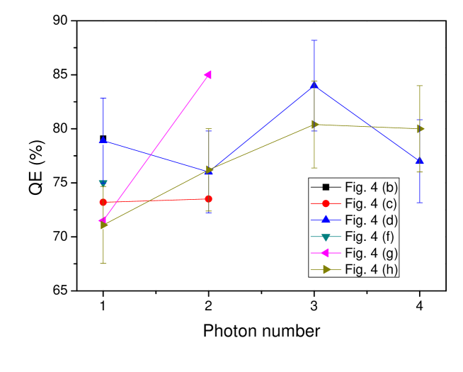
By counting the photon numbers measured within the each number state bin, and considering the Poisson distribution of photons from a laser, the internal quantum efficiency can be calculated. Figure 5 shows the internal quantum efficiency as a function of each photon number state. It can be seen that the quantum efficiency varies from 70 % to 85 % with an error bar about 5 %, and does not change very much up to 4 photons. This internal quantum efficiency is comparable to that of charge integration photon detectors 9 and slightly lower than that of the superconducting transition-edge sensor 7. It should be noticed that the quantum efficiency here represents the proportion of detected photons for a given number of absorbed photons. This is different from the efficiency of optically generated phonons detected by the transistors: The photon detector counts once when there are phonons absorbed by the transistor, which can be a small percentage of the phonons generated by each photon.
The dark count rate is about 0.08 per second with a discrimination level of 0.25 nA, which is due to the noise from the nanowire devices without passivation. For PNR detectors, the noise equivalent power (NEP) is usually defined as 6, where is the photon energy, is the detection efficiency and is the dark count rate. It gives a NEP for our devices of about . The current responsivity is about 2.6 times of that of quantum dot gated field-effect transistors for the detection of one photon 5. We noticed that the NEP can be as low as , when the light is shining directly on one transistor. However, a single transistor device is not practical for photon detection because of the small absorption area. This high sensitivity is due to the following reasons: At a low temperature (less than 10 K), the generated acoustic phonons dissipate ballistically at the speed of sound 24. Because of the anisotropy of the GaAs crystal structure, the phonon phase and group velocities are not colinear, resulting in a phonon focusing effect 25, 13, 26. Karl et al. 27 observed the phonon focusing pattern on the 2DEG by measuring the phonon-drag voltage pattern. When light impinges on the 2DEG, the generated phonons propagate along the {100} planes and {110} planes, which correspond to the fast transverse phonons and slow transverse photons, respectively. In this work, the detection devices were patterned along the [100] direction, as shown in Figure 1 (a).
Another reason for this high responsivity might be due to resonant excitation. For Si -doped GaAs, the main luminescence peak is around 830 nm at 8 K, which is ascribed to a donor to Si acceptor transition. The energy difference between the laser diode (808 nm) and the main luminescence peak is around 37 meV, which is similar to the optical phonon energy (around 36 meV) in GaAs. The phonon emission can be enhanced at this resonant condition because of the resonant enhancement of inelastic light scattering by the 2DEG 28, 29.
In conclusion, we have demonstrated an ultra-high sensitivity photon detector using -doped GaAs based devices, mediated by phonons. The photon number can be resolved up to 4 photons with an accuracy of 855 %. The responsivity is around A/W, where the NEP is about . The internal quantum efficiency is measured to be around 80%. Overall, we believe this phonon mediated optical sensor offers a new approach for highly sensitive photon detectors using semiconductor-based devices.
We acknowledge Dr Andrew Armour and Dr Hongwei Li for very helpful discussions and comments.
References
- Takesue et al. 2007 Takesue, H.; Nam, S. W.; Zhang, Q.; Hadfield, R. H.; Honjo, T.; Tamaki, K.; Yamamoto, Y. Nature Photonics 2007, 1, 343
- Konstantatos et al. 2006 Konstantatos, G.; Howard, I.; Fischer, A.; Hoogland, S.; Clifford, J.; Klem, E.; Levina, L.; Sargent, E. H. Nature 2006, 442, 180
- Divochiy et al. 2008 Divochiy, A.; Marsili, F.; Bitauld, D.; Gaggero, A.; Leoni, R.; Mattioli, F.; Korneev, A.; Seleznev, V.; Kaurova, N.; Minaeva, O.; Gol’tsman, G.; Lagoudakis, K. G.; Benkhaoul, M.; Levy, F.; Fiore, A. Nature Photonics 2008, 2, 302
- Bell et al. 2007 Bell, M.; Antipov, A.; Karasik, B.; Sergeev, A.; Mitin, V.; Verevkin, A. IEEE Trans. Appl. Supercond. 2007, 17, 289
- Gansen et al. 2007 Gansen, E. J.; Rowe, M. A.; Greene, M. B.; Rosenberg, D.; Harvey, T. E.; Su, M. Y.; Hadfield, R. H.; Nam, S. W.; Mirin, R. P. Nature Photonics 2007, 1, 585
- Miller et al. 2003 Miller, A. J.; Nam, S. W.; Martinis, J. M.; Sergienko, A. V. Appl. Phys. Lett. 2003, 83, 791
- Rosenberg et al. 2005 Rosenberg, D.; Lita, A. E.; Miller, A. J.; Nam, S. W. Phys. Rev. A 2005, 71, 061803
- Waks et al. 2004 Waks, E.; Diamanti, E.; Sanders, B. C.; Bartlett, S. D.; Yamamoto, Y. Phys. Rev. Lett. 2004, 92, 113602
- Fujiwara and Sasaki 2007 Fujiwara, M.; Sasaki, M. Apllied Optics 2007, 46, 3069
- Buzhan et al. 2006 Buzhan, P.; Dolgoshein, B.; Filatov, L.; Ilyin, A.; Kaplin, V.; Karakash, A.; Klemin, S.; Mirzoyan, R.; Otte, A.; Popova, E.; Sosnovtsev, V.; Teshima, M. Nuclear Instruments and Methods in Physics Research A 2006, 567, 78
- Kardynal et al. 2008 Kardynal, B. E.; Yuan, Z. L.; Shields, A. J. Nature Photonics 2008, 2, 425
- Clifford et al. 2009 Clifford, J. P.; Konstantatos, G.; Johnston, K. W.; Hoogland, S.; Levina, L.; Sargent, E. H. Nature Nanotechnology 2009, 4, 40
- Bron 1984 Bron, W. E. Nonequilibrium Phonon Dynamics; Plenum Press: New York, 1984
- Baumberg and Williams 1996 Baumberg, J. J.; Williams, D. A. Phys. Rev. B 1996, 53, R16140
- Mizuno and ichiro Tamura 2002 Mizuno, S.; ichiro Tamura, S. Appl. surf. Sci. 2002, 190, 200
- Kato 1997 Kato, H. J. Acoust. Soc. Am. 1997, 101, 1380
- Dzurak et al. 1992 Dzurak, A. S.; Ford, C. J. B.; Kelly, M. J.; Pepper, M.; Frost, J. E. F.; Ritchie, D. A.; Jones, G. A. C.; Ahmed, H.; Hasko, D. G. Phys. Rev. B 1992, 45, 6309
- Schinner et al. 2009 Schinner, G. J.; Tranitz, H. P.; Wegscheider, W.; Kotthaus, J. P.; Ludwig, S. Phys Rev. Lett. 2009, 102, 168801
- Blencowe 1996 Blencowe, M. P. J. Phys.: Condens. Matter 1996, 8, 3121
- Blencowe and Shik 1996 Blencowe, M. P.; Shik, A. Phys. Rev. B 1996, 54, 13899
- Asche et al. 1992 Asche, M.; Friedland, K.-J.; Kleinert, P.; Kostial, H. Semicond. Sci. Tech. 1992, 7, 923
- Poplavsky et al. 2000 Poplavsky, D.; Danilchenko, B.; Kostial, H. Phys. Rev. B 2000, 61, 10941
- Kent et al. 1997 Kent, A. J.; Naylor, A. J.; Hawker, P.; Henini, M.; Bracher, B. Phys. Rev. B 1997, 55, 9775
- Kent et al. 1996 Kent, A. J.; Strickland, R. E.; Strickland, K. R.; Henini, M. Phys. Rev. B 1996, 54, 2019
- Taylor et al. 1971 Taylor, B.; Maris, H. J.; Elbaum, C. Phys. Rev. B 1971, 3, 1462
- Wolfe 1998 Wolfe, J. P. Imaging Phonons; Cambridge University Press: Cambridge, 1998
- Karl et al. 1988 Karl, H.; Dietsche, W.; Fischer, A.; Ploog, K. Phys. Rev. Lett. 1988, 61, 2360
- Danan et al. 1989 Danan, G.; Pinczuk, A.; Valladares, J. P.; Pfeiffer, L. N.; West, K. W.; Tu, C. W. Phys. Rev. B 1989, 39, 5512
- Nakayama et al. 2007 Nakayama, M.; Mizoguchi, K.; Kojima, O.; Furuichi, T.; Mizumoto, A.; Saito, S.; Syouji, A.; Sakai, K. Phys. Stat. Sol. (a) 2007, 204, 518