Electron transport in waveguides
with spatially modulated strengths of the Rashba
and Dresselhaus terms of the spin-orbit interaction
Abstract
We study electron transport through waveguides (WGs) in which the strengths of the Rashba () and Dresselhaus () terms of the spin-orbit interaction (SOI) vary in space. Subband mixing, due to lateral confinement, is taken into account only between the two first subbands. For sufficiently narrow WGs the transmission exhibits a square-like shape as a function of or . Particular attention is paid to the case of equal SOI strengths, , for which spin-flip processes are expected to decrease. The transmission exhibits resonances as a function of the length of a SOI-free region separating two regions with SOI present, that are most pronounced for . The sign of strongly affects the spin-up and spin-down transmissions. The results show that the main effect of subband mixing is to shift the transmission resonances and to decrease the transmission from one spin state to another. The effect of possible band offsets between regions that have different SOI strengths and effective masses is also discussed.
pacs:
71.10.Pm, 72.25.-b, 73.21.-bI Introduction
There has been growing interest in the studies of spin-orbit interaction (SOI) in low-dimensional semiconductor structures made of III-V materials. The spin degree of freedom, often neglected in transport studies in semiconductors like silicon or germanium, may be important in other materials depending on the crystal structure, growth condition, and band alignment of the whole heterostructure. SOI, of relativistic origin, is a coupling between the intrinsic angular momentum (spin) and the orbital angular momentum in an external electric field. SOI manifests itself in semiconductor structures either due to the lack of (macroscopic) inversion symmetry of the whole structure, referred to as the Rashba SOI term bych , or due to the lack of inversion symmetry of the crystal structure, referred to as the Dresselhaus SOI term wink ; dres . The Rashba term can also be viewed as an effective magnetic field in the local frame, perpendicular to both momentum and electric field. Apart from the band alignement, it also depends on any external potential if it lifts the overall inversion symmetry which means it can be tuned by applying a bias nit ; gate2 ; gate3 . On the other hand, the Dresselhaus SOI (DSOI) term arises as a consequence of the lack of inversion symmetry of the underlying crystal structure. It is commonly present in III-V semiconductors, like GaSb that has the zinc-blende structure, where the difference between cations and anions breaks the degeneracy of the band structure with respect to the spin degree of freedom, and is present in both bulk materials and semiconductor nanostructures. In low-dimensional semiconductor structures the DSOI manifests itself through terms that are linear and cubic in the wave vector ; here we consider only the former, which is dominant for small and is referred to as the linear Dresselhaus term. There is an additional source of spin splitting present in semiconductor heterostructures due to the reduced symmetry at the interface Ivch ; Krebs . This manifestation of spin-orbit coupling is often named interface inversion symmetry or interface Dresselhaus SOI Gan2 .
The studies of spin-dependent phenomena in semiconductor structures have been particularly intensified after the proposal of a spin-field effect transistor (FET) by Datta and Das Datta . This kind of the device would make use of the Rashba SOI only, by controlling the electron spin during its passage through the transistor. Ever since this proposal, there have been many refinements of the idea, notably the non-ballistic spin field-effect transistor schl1 which would utilize both the Rashba and Dresselhaus terms of equal strength. In this design it is expected that the transistor is robust against spin-indepedent scattering mechanisms. Further, a modification of the Datta-Das device has been proposed SFET_DSO whose function would be based on solely the DSOI. Motivated by this idea a wealth of related studies appeared in similar systems that dealt with spin-dependent transport, see, e.g, the review paper zut .
In previous work, coauthored by one of us, ballistic transport and spin-transistor behavior was studied, due only to the RSOI, in stubbed wan1 WGs with constant strength or unstubbed WGs with periodically modulated wan2 . An encouraging result was a nearly square-wave form of the transmission as a function of some stub parameters wan1 or the strength wan2 . In this work we extend these studies by treating simultaneously both SOI terms, taking into account mixing between the lowest two subbands, and by studying longitudinal transmission resonances that occur when the length of a SOI-free region, separating two regions with SOI present, varies. As will be seen, if only one subband is occupied and both SOI terms are present, a phase difference arises in the spin eigenfunctions that strongly affects the spin-up and spin-down transmissions especially when changes sign. In Sec. II we present a model of a WG with two subbands, due to a lateral confinement, having nonzero mixing. We also derive the relevant dispersion relations and one-electron wave functions. In Sec. III we briefly explain the numerical procedure and present the main results. Concluding remarks follow in Sec. IV.
II Theoretical model

One unit of the WG we consider is shown in Fig. 1. It is made, e.g., of two layers of InxGa1-xAs with different content of In, , and has SOI strengths and . The WG consists of a finite number of such units periodically repeated in the direction. Along the direction a confining potential is present that gives rise to bound states having energies . In principle a confinement along could be created by etching after the usual 2D one along . The two different growth directions which will be discussed are and .
II.1 grown waveguide
The one-electron Hamiltonian reads
| (1) |
where is given by
| (2) |
Here is the wavevector of the electron and its effective mass. and are the Rashba and Dresselhaus terms, respectively, given by
| (3) |
where are the Pauli spin matrices, and , the strengths of the Rashba and Dresselhaus terms, respectively. In writing Eq. (3) we assumed that the strength depends mainly on the confinement along the axis, only the linear-in-wave vector Dresselhaus term is important, and neglected any dependence on the lateral confinement along the axis. The idea of linearly changing by changing the well width along has recently been reconfirmed in Ref. jak, .
We write the total wave function as a linear combination of eigenstates of the unperturbed Hamiltonian
| (4) |
with labelling the discrete subbands due to the confining potential . The unperturbed states satisfy , with and . is the solution of
| (5) |
with the square-type assumed high enough so that at the edges of the WG.

Using the full Hamiltonian given by Eqs. (1)-(3) and setting and , Eq. (4) leads to the secular equation
| (6) |
The factor embodies the subband mixing due to confinement and is nonzero for ,
| (7) |
To assess the magnitude of subband mixing we assume that the confining potential is that of a quantum well with infinitely high walls at the edges of the WG whose width is . Then and considering mixing between the lowest two subbands the only non-vanishing matrix elements are , with wan1 . Under these assumptions the eigenvalue problem resulting from Eq. (6) takes the form
| (8) |
where . The eigenenvalues, readily found from Eq. (19), are
| (9a) | |||
| (9b) | |||
| (9c) | |||
| (9d) |
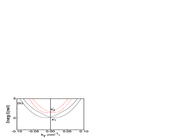
with , (), and . The energy dispersions are given in the left panel of Fig. 2 for and in the right one for .
Note that the energy dispersion curves do not start from , at but rather from
| (10a) | |||
| (10b) |
where , as a result of the subband mixing.
Analytical expressions for the wavevector as a function of the energy are complicated for the general case . Particular attention will be paid to the case in which a suppression of spin-flip processes is expected schl1 ; Golub . The relevant expressions are
| (11a) | |||
| (11b) |
that determine the nature of the wave vectors in the following manner:
for fixed () all solutions are complex and conjugate in pairs;
the solutions are real and the ones complex conjugate;
all solutions are real.
For vanishing Dresselhaus strength , the eigenvalue problem Eq. (19) simplifies significantly and the eigenvectors
acquire Wangsubbmix the simple analytical form
| (14a) | |||
| (14b) |
where , , , and . Further, , , and .
If one goes further and neglects subband mixing, by taking the limit , and if only the first subband is occupied, the original eigenvalue problem, Eq. (19), reduces essentially to a problem. Then the energy spectrum is given by
| (15) |
and the spinors acquire the simple form
| (16) |
This form of the spinors is important for the analysis of the transport problem through WGs. More precisely, one easily sees that the effect of the presence of the DSOI term is not just a simple increase of the overall SOI coupling, that is, in place of ; one also has the change in the phase of the spinor component, that may significantly alter the transmission from one spin state to another. For illustrative purposes, we derive an analytical expression for the total transmission through a simple WG segment, with equal SOI strengths () and length , sandwiched between two SOI-free segments. The result is
| (17) |
where , , , and . Once again, the effect of having both SOI terms present is not limited to the replacement ; the transmission amplitude is also modulated through the factor in Eq. (17), if one compares with the simplest case () wan2 . From now on we will evaluate the transmission of spin states with being the quantization axis.
II.2 Waveguide grown along the direction
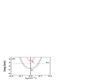
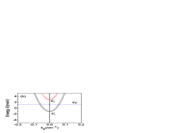
Apart from the usual growth direction along the crystallographic axis , the growth along the direction is also important to investigate. The Dresselhaus term has a somewhat simpler form Dres110
| (18) |
while the Rashba term retains the same form since it is related to the structural (macroscopic) inversion asymmetry anothWang . Employing a procedure similar to that in Sec. III A, we arrive at the eigenvalue problem
| (19) |
where the notation is the same as in Eq. (8).
The eigenenvalues, readily found from Eq. (19), are given by Eq. (9) with and replaced, respectively, by and . The energy dispersions are given on the left panel of Fig. 3 for and on the right one for . The dispersion curves are qualitatively different than those pertaining to the direction due to the different form of the Dresselhaus term . Further, the difference between equal and unequal SOI strengths is not as drastic as for WGs grown along the direction.
III Numerical procedure and results
As shown in Fig. 1, the WG consists of two segments, with different values of the Rashba and Dresselhaus couplings and , periodically repeated along the axis. In each of the segments the wave vector is constant so that the wave function in the -th segment is a superposition of plane wave-like states consisting of the eigenvectors () of Eq. (19), in both directions along the axis
| (20) |
where . To find the complete solution, we first match the wave function at the interfaces between the and segments. Due to the presence of the off-diagonal elements in the Hamiltonian the continuity of the derivative of the wave function may not hold. A more general procedure is to require that the flux through materials with different SOI strengths or/and effective masses be conserved mol . The velocity operator is given by
| (21) |
The continuity of the wave function at the interface gives and that of the flux . The unknown coefficients from Eq. (20) from one segment to another can be related through the transfer-matrix formalism by introducing the propagation matrix and the boundary matching matrix in each segment . The transfer matrix Xu for the -th segment is the matrix product
| (22) |

In all numerical calculations we assumed that the incident electrons are (spin) unpolarized and we investigate only the transmission of one spin state, for instance, the spin-up one. We take the axis as the quantization axis. We measure the SOI strengths in units of eVm (Ref. gate3 ) and we first consider an energy meV+ below the second subband.


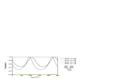
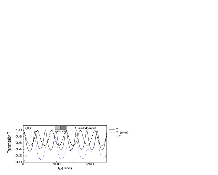
First, we investigate the electron transmission through two segments having equal SOI strengths and being separated by a SOI-free region of length . The results are shown in Fig. 4 for several cases: (1) and have the same sign in both segments; the total transmission is shown by the solid curve and the transmission from the spin-up to the spin-down state by the dotted curve; (2) the same as in case (1) but with negligible subband mixing (, solid dashed curve); (3) in the second segment and shown by the dash-dotted curve. We note that the total transmission is the same in cases (1) and (3), only the spin-up and spin-down transmissions are different in these cases. Here the value of is taken to be , close to the experimental value given in Ref. nit . It can be inferred that changing the sign of suppresses the transmission to the opposite spin state, while the subband mixing shifts the resonance maxima and has a minimal effect on the shape of the curve.
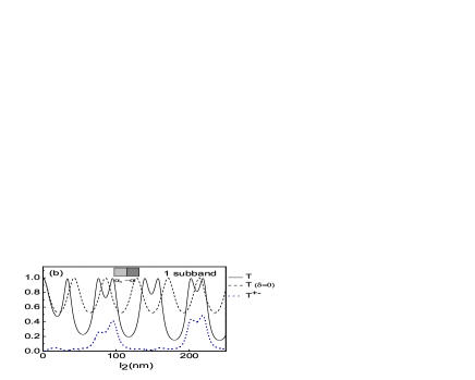
In Fig. 5 we plot the total transmission through units, as a function the length , for fixed nm and in the SOI-free region, see Fig. 1, in two arrangements: with subband mixing present in panel (a) and absent () in panel (b). For illustrative purposes here we take . Comparing the two graphs, one notices that the subband mixing introduces aperiodic features mainly in the transmission. Inspecting Fig. 5(b), one sees the effect of increasing : the minima become deeper and shifted to the left.
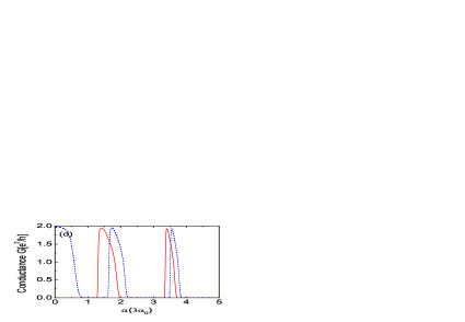
It would be useful to investigate transport through a WG with significantly more than several units. The transmission through units is shown in Fig. 6(a) and Fig. 6(c), as a function of the ratio . In panels (a) and (b) the SOI strengths are given in units of and those in panels (c) and (d) in units of . For a clearer comparison the unit lengths nm and the energy meV are the same in all panels. Also, in all cases the SOI is absent in the first segment of the unit. Only ballistic transport was considered and the aim of taking a large number of units, , is to demonstrate the near binary behaviour of the transmission last . This is readily seen by contrasting the upper with the lower panels. Notice though that the lower panels involve rather big SOI strengths.
Apart from the transmission , the conductance provides valuable information about the nanostructure especially at finite temperatures. is given by the standard expression
| (23) |
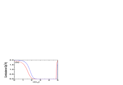
where is the Fermi-Dirac distribution. In Fig. (6)(b)
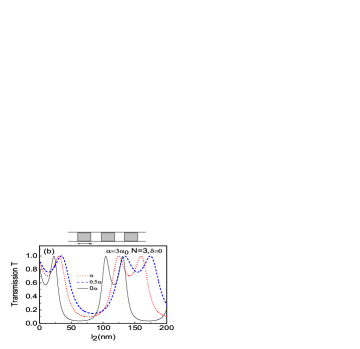
we show for the same WG, at finite temperature K, as a function of with kept constant and equal, respectively, to and (solid red curves), and (dashed blue curves). As can be seen, the dashed and dotted curves coincide since the SOI strength is the same in units of . The conductance when or starts from since then the WG is completely transparent (no SOI), whereas when both SOI terms are present starts from a value between and due to phase and a non-trivial energy dispersion , see Eqs. 15 and (16). In all cases the first segment of the unit has zero SOI. For higher values of the SOI strengths, (dashed curve in Fig. 6(d)) the conductance exhibits a more binary behavior. For higher temperatures the qualitative behavior of remains the same but the dips get shallower. We now assess the dependence of the transmission on the phase . In Fig. 7 we show through two successive WG segments, with the same length and strength , versus . Panel (a) is for and panel (b) for . The solid curves show the total transmission while the dotted ones correspond to . For comparison, the values of the total transmission for zero mixing () are shown as dashed curves. Comparing the two graphs one sees a strong effect the change of the sign of has on the spin-down contribution which is almost filtered out for and smaller than about nm as well as for approximately in the range nm nm .
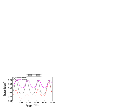
At this point one may wonder how realistic the difference in SOI strengths is from one region to another or how it can be changed. Firstly, one can use the same material throughout the WG and instead apply gates that can change , from region 1 to region 2, by a factor of 2 to 5. Secondly, if one uses different materials for regions 1 and 2, a band offset exists between them, i.e., is not everywhere zero. As is well known, the Rashba term is controlled by an external gate and is taken to be zero within the layer made of InGaAs. That is, one can take but keep in the first segment, since it was assumed that . As usual we take for InGaAs. In Fig. 8(a) we show the case when the two InGaAs segments are separated by a pure GaAs segment (), free of the Rashba SOI, as a function of the separation length . For an indium content , the conduction band mismatch between pure GaAs and InxGa1-xAs is experimentally determined Lu to be . In
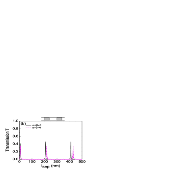
Fig. 8(b) we show the transmission through two InGaAs () segments separated by a RSOI-free segment but now made of InGaAs with .
In the case we consider, , we assume , for . The effective masses of In0.2Ga0.8As and In0.1Ga0.9As are and , respectively effmassInGaAs . We have taken into account this effective-mass difference between the two materials through the matching of the flux at the interfaces. The solid and dashed-dotted curves show the total transmission with and without SOI present, respectively. As shown, with a band offset present the transmission is smaller. The higher content of indium results in narrower transmission peaks when plotted vs . In both cases, the peak-to-valley ratio is enhanced by the presence of SOI, thus improving the performance of a WG as a possible transistor. We further notice that, although the band offset is large compared to the change in the conduction-band structure caused by the SOI, in the order of a few , the influence of the SOI, through the phase factor in Eq. (16), is still important and changes the period of the transmission.
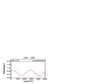
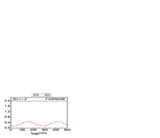
Next, we consider the situation when both subbands are occupied, which occurs for . The electron transmission was evaluated through two simple units () separated by a SOI-free region of length . The total transmission (solid curve) and the transmission from the spin-up to the spin-down state (dashed curve) of the second subband are shown in Fig. 9(a), when both units have positive strength , and in Fig. 9(b) when the second unit has a negative . In both cases the total transmission is close to unity, as a result of the high value of the Fermi energy, meV, while the value of is suppressed when the Rashba coupling changes sign as in the case of only one subband occupied, see Fig. 4. One can see the filtering effect only in particular components of the transmission, while the total transmission varies very little with . We emphasize that the shape and values of are more sensitive to changes in the energy and the strength than in the case when only one subband is occupied.

Finally, we consider a WG grown along the direction that was treated theoretically in Sec. II.2. The Dresselhaus term acquires the simple form and, as was shown in Sec. III, this affects the dispersion relation significantly. We show numerical results for the transmission through two InGaAs segments separated by a Rashba SOI-free region in Fig. 10 when only one subband is occupied. The solid curve shows the total transmission and the dotted one, barely visible, the transmission. . As seen, the peak values are noticeably lower than in the previous case and the number of peaks is increased due to the different dispersion relation .
IV Concluding remarks
We presented results for the electron transmission through WGs in which both terms of the SOI are present and the mixing of the first two subbands is taken into account. In general, the influence of subband mixing is to shift the (longitudinal) resonances and suppress the spin-down to spin-up transmission. Two growth directions were considered and , with more attention given to the former. Further, changing the sign of the RSOI strength has a very strong filtering effect on the spin-down contribution while leaving the total transmission intact.
For two segments separated by a SOI-free region, of length , shows resonances, as a function of , that are most pronounced for . When both subbands are occupied, the total transmission varies little and remains close to unity, so that the filtering effect is contained only in . Similar to the case when one subband is occupied, changing the sign of the Rashba strength reduces the spin-up to spin-down transmission, cf. Fig. 9. In addition, we took into account possible band offsets between these segments and the SOI-free region that separates them. As shown in Fig. 8, this reduces the amplitude of the transmission but does not affect its qualitative dependence on , notice in particular the highly binary structure of the transmission in Fig. 8(b) and consequently that of the conductance (not shown) at least for very low temperatures as reflected by Eq. (23).
The transmission and conductance oscillate as a function of , , or if and are sufficiently strong. In such a case a nearly square-wave form is shown in Fig. 6(c) for and in Fig. 6(d) for at temperature K. Both results are in line with those wan2 for . For higher temperatures the qualitative behaviour of remains the same but its maxima are a bit rounded off. Together with the control of by a bias nit and the independent one of reported very recently jak , the results indicate that a realistic spin transistor is possible if the SOI-free regions are relatively narrow.
Acknowledgements.
Our work was supported by the Canadian NSERC Grant No. OGP0121756.References
- (1) Y. A. Bychkov and E. I. Rashba, J. Phys. C 17, 6039 (1984).
- (2) R. Winkler, Spin-orbit coupling effects in two-dimensional electron and hole systems, Springer Tracts in Modern Phys. Vol. 191 (Springer, New York, 2003).
- (3) G. Dresselhaus, Phys. Rev. 100, 580 (1955).
- (4) J. Nitta, T. Akazaki, H. Takayanagai, and T. Enoki, Phys. Rev. Lett. 78, 1335 (1997); C-M Hu, J. Nitta, T. Akazaki, H. Takayanagi, J. Osaka, P. Pfeffer and W. Zawadzki, Phys. Rev. B 60, 7736 (1999).
- (5) G. Engels, J. Lange, T. Schäpers and H. Lüth Phys. Rev. B 55 R1958 (1997).
- (6) D. Grundler, Phys. Rev. Lett. 84, 6074 (2000).
- (7) E. L. Ivchenko, A. Y. Kaminski, and U. Rössler, Phys. Rev. B 54, 5852 (1996).
- (8) O. Krebs, D. Rondi, J. L. Gentner, L. Goldstein, and P. Voisin, Phys. Rev. Lett. 80, 5770 (1998).
- (9) S. D. Ganichev, V. V. Bel’kov, L. E. Golub, E. L. Ivchenko, P. Schneider, S. Giglberger, J. Eroms, J. De Boeck, G. Borghs, W. Wegscheider, D. Weiss, and W. Prettl, Phys. Rev. Lett. 92, 256601 (2004); V. I. Perel , S. A. Tarasenko, I. N. Yassievich, S. D. Ganichev, V. V. Bel kov, and W. Prettl, Phys. Rev. B 67, 201304(R) (2003).
- (10) S. Datta and B. Das, Appl. Phys. Lett. 56, 665 (1990).
- (11) J. Schliemann, J. C. Egues, and D. Loss, Phys. Rev. Lett. 90, 146801 (2003).
- (12) S. Bandyopadhyay and M. Cahay, Appl. Phys. Lett. 85, 1814 (2004).
- (13) I. Žutić, J. Fabian, and S. Das Sarma, Rev. Mod. Phys. 76, 323 (2004).
- (14) X. F. Wang, P. Vasilopoulos, and F. M. Peeters, Phys. Rev. B 65, 165217 (2002).
- (15) X. F. Wang and P. Vasilopoulos, Appl. Phys. Lett. 83, 940 (2003).
- (16) J. D. Koralek, C. Weber, J. Orenstein, A. Bernevig, S. Zhang, S. Mack, and D. Awschalom, Nature 458, 610 (2009).
- (17) N. S. Averkiev and L. E. Golub, Phys. Rev. B 60, 15582 (1999).
- (18) X. F. Wang and P. Vasilopoulos, Phys. Rev. B 68, 035305 (2003).
- (19) X. Cartoixà, L.-W. Wang, D. Z.-Y. Ting, Y.-C. Chang, Phys. Rev. B 73, 205341 (2006); B. A. Bernevig, J. Orenstein, and S.-C. Zhang, Phys. Rev. Lett. 97, 236601 (2006); M.-H. Liu, K.-W. Chen, S.-H. Chen, and C.-R. Chang, Phys. Rev. B 74, 235322 (2006).
- (20) M. Wang, K. Chang, and K. S. Chan, Appl. Phys. Lett. 94, 052108 (2009).
- (21) L. W. Molenkamp, G. Schmidt, and G. E. W. Bauer, Phys. Rev. B 64, 121202(R) (2001).
- (22) H. Xu, Phys. Rev. B 47, 9537 (1993).
- (23) For the total length of the structure is and comparable to the phase relaxation length which is about , see Choi et al. Phys. Rev. B 36, 7751 (1987). For larger the implicit assumption will not hold but one could reduce the unit length to satisfy this condition.
- (24) L. Lu, J. Wang, Y. Wang, W. Ge, G. Yang, and Z. Wang, J. Appl. Phys. 83, 2093 (1998).
- (25) J. C. Fan and Y. F. Chen, J. Appl. Phys. 80, 6761 (1996).