Conductance of correlated systems: real-time dynamics in finite systems
Abstract
Numerical time evolution of transport states using time dependent Density Matrix Renormalization Group (td-DMRG) methods has turned out to be a powerful tool to calculate the linear and finite bias conductance of interacting impurity systems coupled to non-interacting one-dimensional leads. Several models, including the Interacting Resonant Level Model (IRLM), the Single Impurity Anderson Model (SIAM), as well as models with different multi site structures, have been subject of investigations in this context. In this work we give an overview of the different numerical approaches that have been successfully applied to the problem and go into considerable detail when we comment on the techniques that have been used to obtain the full I–V-characteristics for the IRLM. Using a model of spinless fermions consisting of an extended interacting nanostructure attached to non-interacting leads, we explain the method we use to obtain the current–voltage characteristics and discuss the finite size effects that have to be taken into account. We report results for the linear and finite bias conductance through a seven site structure with weak and strong nearest-neighbor interactions. Comparison with exact diagonalisation results in the non-interacting limit serve as a verification of the accuracy of our approach. Finally we discuss the possibility of effectively enlarging the finite system by applying damped boundaries and give an estimate of the effective system size and accuracy that can be expected in this case.
pacs:
73.63.-b, 72.10.Bg, 71.27.+a, 73.63.KvI Overview
During the past decade improved experimental techniques have made the production of and measurements on one-dimensional systems possible Sohn et al. (1997), and hence led to an increased theoretical interest in these systems. However, the description of non-equilibrium transport properties, like the finite bias conductance of an interacting nanostructure attached to leads, is a challenging task. In general, for non-interacting particles, the conductance can be extracted from the transmission of the single particle levels Landauer (1957, 1970); Büttiker (1986). For interacting particles in small or low-dimensional structures where the screening of electrons is reduced, electron-electron correlations can no longer be neglected. Recently several methods to calculate the zero bias conductance of strongly interacting nanostructures have been developed. One class of approaches consists in extracting the conductance from an easier to calculate equilibrium quantity, e.g. the conductance can be extracted from a persistent current calculation Sushkov (2001); Molina et al. (2003); Meden and Schollwöck (2003); Molina et al. (2004); Freyn et al. (2009), from phase shifts in NRG calculations Oguri et al. (2005), or from approximations based on the tunneling density of states Meir et al. (1991). Alternatively one can evaluate the Kubo formula within Monte-Carlo simulations Louis and Gros (2003), or from DMRG calculations Bohr et al. (2006); Bohr and Schmitteckert (2007); Schmitteckert and Evers (2008). Linear conductance has also been investigated using Functional Renormalization Group studies Karrasch et al. (2006), or by diagonalizing small clusters and attaching them to leads via a Dyson equation Büsser et al. (2000).
In contrast, there are only a few methods available to get rigorous results for the finite bias conductance. While the problem has been formally solved by Meir and Wingreen using Keldysh Greens functions Meir and Wingreen (1992), the evaluation of these formulas for interacting systems is generally based on approximations such as real time Keldysh RG Schoeller and König (2000). Within the framework of time dependent density functional theory (td-DFT) and Keldysh Greens functions Stefanucci and Almbladh Stefanucci and Almbladh (2004b, a) discuss the extraction of conduction from real time simulations. The restriction to finite sized systems for calculating transport within td-DFT was also discussed by Di Ventra and Todorov Di Ventra and Todorov (2004). In Bushong et al. (2005) Bushong, Sai, and Di Ventra discuss the extraction of a finite bias current similar as discussed below in the framework of td-DFT. Weiss, Eckel, Thorwart and Egger Weiss et al. (2008) discuss an iterative method based on the summation of real-time path integrals (ISPI) in order to address quantum transport problems out of equilibrium. Han and Heary Han and Heary (2007) discuss strongly correlated transport in the Kondo regime using imaginary time Quantum Monte Carlo techniques.
In this work we review the concept of calculating the finite bias conductance of nanostructures based on real time simulations Cazalilla and Marston (2002); Luo et al. (2003); Daley et al. (2004); White and Feiguin (2004); Schmitteckert (2004); Feiguin and White (2005); Schneider and Schmitteckert (2006); Schmitteckert (2007); Ulbricht and Schmitteckert (2008); Branschädel et al. (2009); Al-Hassanieh et al. (2006); Boulat et al. (2008); Heidrich-Meisner et al. (2009a, b); Kirino et al. (2008); da Silva et al. (2008) within the framework of the DMRG White (1992, 1993); Noack and Manmana (2005); Hallberg (2006); Schollwöck (2005). It provides a unified description of strong and weak interactions and works in the linear and finite bias regime, as long as finite size effects are treated properly. The method was successfully applied to obtain results for the finite bias conductance in the interacting resonant level model, showing perfect agreement with analytical methods based on the Bethe ansatz Boulat et al. (2008). I–V-characteristics have been obtained for the single-impurity Anderson model using the adaptive td-DMRG-method Heidrich-Meisner et al. (2009a). Finite size effects and especially the impact of the possible combinations of tight binding leads with an even or odd number of sites coupled to the structure have been studied in detail in Heidrich-Meisner et al. (2009b) for a single impurity and for three quantum dots. Here, we show that finite size effects can be directly related to the structure of the single particle energy levels in non-interacting systems.
In a first approach of time dependent dynamics within DMRG, Cazalilla and Marston integrated the time-dependent Schrödinger equation in the Hilbert space obtained in a finite lattice ground state DMRG calculation Cazalilla and Marston (2002). Since this approach does not include the density matrix for the time evolved states, its applicability is very limited. Luo, Xiang and Wang Luo et al. (2003) improved the method by extending the density matrix with the contributions of the wave function at intermediate time steps, restricting themselves to the infinite lattice algorithm. Schmitteckert Schmitteckert (2004) showed that the calculations can be considerably improved by replacing the integration of the time dependent Schrödinger equation with the evaluation of the time evolution operator using a Krylov subspace method for matrix exponentials and by using the full finite lattice algorithm.
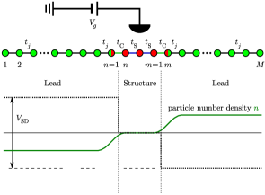
 attached to non-interacting leads
  (finite interaction with the first lead site
 allowed) and schematic
density profile (green solid line) of the -particle wavepacket at initial time .
The density profile corresponds to the -particle ground state of the Hamiltonian
, cf. Eq. (7), where the bias voltage enters as
a local chemical potential (black dotted line).
allowed) and schematic
density profile (green solid line) of the -particle wavepacket at initial time .
The density profile corresponds to the -particle ground state of the Hamiltonian
, cf. Eq. (7), where the bias voltage enters as
a local chemical potential (black dotted line).An alternative approach is based on wave function prediction White (1996). There one first calculates an initial state with a static DMRG. One iteratively evolves this state by combining the wave function prediction with a time evolution scheme. In contrast to the above mentioned full td-DMRG, one only keeps the wave functions for two time steps in each DMRG step. Different time evolution schemes have been implemented in the past using approximations like the Trotter decomposition Daley et al. (2004); White and Feiguin (2004); Al-Hassanieh et al. (2006), or the Runge-Kutta method Feiguin and White (2005). Schneider and Schmitteckert Schneider and Schmitteckert (2006); Schmitteckert and Schneider (2006) combined the idea of the adaptive DMRG method with direct evaluation of the time evolution operator via a matrix exponential using Krylov techniques as described in Ref. Schmitteckert (2004). Therefore the method involves no Trotter approximations, the time evolution is unitary by construction, and it can be applied to models beyond nearest-neighbor hopping.
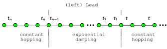
Concerning finite size effects, damped boundary conditions have been applied in order to obtain an increased effective system size in the regime of small bias voltage Bohr et al. (2006); Kirino et al. (2008); da Silva et al. (2008), where an improved scheme for linear conductance was presented in Bohr and Schmitteckert (2007). In the non-interacting case this can be traced back to a shift of the discrete single particle energy levels of the system towards the center of the cosine band. We demonstrate that this procedure can also be used when applying bias voltage of the order of magnitude of the band width when handled carefully.
II The System
The Hamiltonian for the nanostructure is given by (S: the structure itself, L: leads, C: contacts)
| (1) |
| (2) | |||||
| (3) | |||||
| (4) | |||||
where . Individual sites are labeled according to Fig. 1, is the size of the interacting nanostructure, denotes a local external potential, which can be applied to the nanostructure, is a nearest-neighbor interaction inside the nanostructure, and is a nearest-neighbor interaction with the first lead sites. The hopping elements in the leads, the structure, and coupling of the structure to the leads are , , and , respectively. The hopping parameter in the leads is not necessarily constant to allow for the inclusion of damped boundary-conditions. This can be used to divide the leads in three areas, Fig. 2: here, two regions with constant hopping matrix element and are smoothly coupled via a region of exponential damped hopping, which allows for increasing the resolution of the level spacing of the single particle energy levels on the energy scale . For hard-wall boundary-conditions, however, .
The current operator at an arbitrary bond can be derived from the charge operator using a continuity equation. For the tight-binding Hamiltonian (1) the current operator and its expectation value take the form
| (5) | |||||
We define the current through the nanostructure as an average over the current in the left and right contacts to the nanostructure
| (6) |
III Initial conditions and time evolution
Following the prescription implemented in Schmitteckert (2004); Ulbricht and Schmitteckert (2008) we add an external bias potential, namely the charge operator,
| (7) |
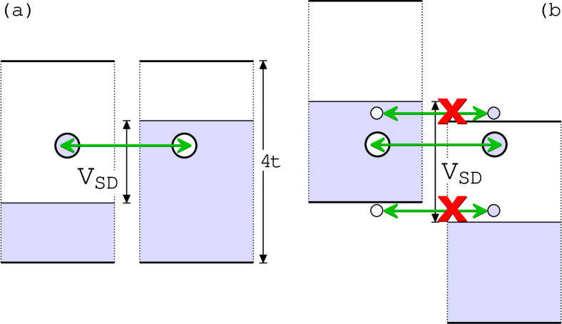
to the unperturbed Hamiltonian and take the ground state of , obtained by a standard finite lattice DMRG calculation, as initial state at time Schmitteckert (2004). The minimization of the energy of the system leads to a charge imbalance in the right (source) and the left (drain) lead corresponding to , as sketched in Fig. 3(a). Alternatively, the bias voltage also can be added to the time evolution. The initial state then has to be obtained as the ground state of the unperturbed Hamiltonian , while the time evolution is performed using , cf. also Fig. 3(b). Starting from , the time evolution of the system results from the time evolution operator with , which leads to flow of the extended wave packet through the whole system until it is reflected at the hard wall boundaries as described in Schmitteckert (2004). Corresponding to the two different schemes introduced before, is given as either (a) or (b) .
The sudden switching of the bias voltage results in a ringing of the current in a transient time regime Wingreen et al. (1993), see also Fig. 4(a). Here we show the short time behavior of the current through a single impurity coupled to two leads in a system with lattice sites in total. This transient behavior with its characteristic oscillations decays on the time scale , where is the width of the conductance peak. By smearing out the voltage drop over a few lattice one may reduce the influence of large momentum states. Furthermore, the finite size of the system leads to reflection of wave packets at the boundaries, cf. Fig. 4(b). A wave packet travelling with Fermi velocity from the impurity towards the boundaries will return to the impurity after a transit time given by , which is the characteristic time scale for finite size effects appearing in the expectation value of time dependent observables.
To compare the approaches (a) and (b), we show current voltage-characteristics in Fig. 5 for the resonant level model with a single impurity (, cf. Fig. 1) coupled to two leads via the hopping matrix element and the gate voltage as well as the interaction set to . The dots correspond to results obtained numerically using exact diagonalisation, while the lines correspond to analytic calculations included for comparison. Here, the straight line shows the current assuming linear scaling with with linear conductance , while the curved line overlaid by the numerical results for approach (a) has been obtained using the Landauer–Büttiker approach, taking cosine-dispersion into account.
The procedure of extracting the current from the numerical data will be described in the next section. Here we want to emphasize the different results we get for the I–V-curve for the two different cases. For the tight binding Hamiltonian the dispersion relation is given by , with a finite band width . For the approach (a) this leads in the non-interacting case to a saturation of for all values of the bias voltage . Further increasing beyond the band edge does not change the initial occupation of energy levels. In contrast, for the case (b), the particles will be distributed equally over the left and the right lead in the initial state , whereas the voltage enters in the time evolution operator. For small values of we find a good agreement for for (a) and (b), while for there is a mismatch which finds its expression in a current maximum for with a subsequent break down to for . This behavior has been predicted in Cini (1980) and can be understood from Fig. 3(b), which explains how energy conservation prevents particles (holes) to tunnel from one lead to the other which removes contributions to the current. 111We want to emphasize that the negative differential conductance for the IRLM with tight binding chains in Boulat et al. (2008) is not related to the band effect described here. In fact, approach (a) has been used there for the numeric simulation while, in contrast, we find saturation of the current in the non-interacting case. In addition the maximum of the current appears at an energy below half the band width, where both approaches give the same result.. More recently, a detailed analysis of the negative differential conductance for the situation (b) has been carried out Bâldea and Köppel (2010). In this work, it has been realised that the density of states in the leads adds a major contribution to the breakdown of the current.
Moreover, there are other approaches to how the initial state and the time evolution can be defined. For example, in addition to prescription (a), the coupling and the interaction can be set to zero for the calculation of . In this case (c), both leads as well as the structure are totally independent systems, and there is a very intuitive connection of and the difference of the particle number in the left and the right lead, because the isolated leads can be described in a single particle picture. The drawback of this approach, which adds a sudden switching of and in addition to the switching of at initial time , is an enhanced transient regime and therefore a reduced plateau of constant current that we need to extract the I–V-curve from. In Fig. 6 we compare the time dependent current obtained using the different initial conditions (a) and (c) for a single impurity coupled to two leads via , including a finite density-density interaction , for different values of . To evaluate the time evolution of a system with finite interaction numerically, we used the td-DMRG method, with parameters as described in the figure caption of Fig. 6. For both approaches (a) and (c), we find a time regime of (quasi) constant current. However, approach (a) has several advantages over (c): the current plateau is more consistent, which simplifies analysis, and to keep the discarded entropy in the td-DMRG calculation below a predefined threshold, the number of states, which have to be kept in the DMRG, is considerably higher for (c) when compared to (a), making approach (c) computationally much more expensive. The latter point is illustrated in Fig. 7, where we compare the maximum dimension of the DMRG projection scheme that is necessary to keep , for different values of the bias voltage , of the gate voltage and of the interaction . We always find a much smaller value of for (a) as compared to (c).
Another problem of approach (c) is the discretization of the I–V-curve into steps resulting from the discrete single particle energy levels of the initial state. This could probably be handled using a procedure similar to the one described in section V.2.
For these reasons we will use approach (a) throughout the remainder of this paper.
IV Differential and linear conductance
For the calculation of the DC-conductance through the nanostructure the time evolution has to be carried out for sufficiently long times until a quasi-stationary state is reached and the steady state current can be calculated. If the stationary state corresponds to a well-defined applied external potential , the differential conductance is given by In the limit of a small applied potential, , the linear conductance is given by
To discuss the general behavior of the time evolution from an initial nonequilibrium state we first consider the most simple case we can think of: transport through a single impurity. The current rises from zero and settles into a quasi-stationary state, Fig. 4(a). After the wavepackets have traveled to the boundaries of the system and back to the nanostructure, the current falls back to zero and changes sign, cf. Fig. 4(b). Additionally there is a third type of finite size oscillations, Fig. 8. Here we show the time dependent current for different configurations, from the leads to the impurity on a single (left or right) contact link, and through the impurity as defined in Eq. (6). After the initial oscillations have decayed on the time scale , the current through a single contact link shows remaining oscillations, with an amplitude depending on and , and proportional to the inverse of the system size . The latter is demonstrated in Fig. 9. The period of the oscillation depends on the applied bias voltage [compare Fig. 8 (b, c)] but is independent of the system size [Fig. 8 (b-d)] and of the gate potential [Fig. 10], and is given by . In the resonant tunneling case [Fig. 8(a), ], the oscillations on the left and the right contact link cancel in the current average Eq. (6) due to a different sign in the amplitude of the oscillations , which does not hold in general [Fig. 8(b-d), ], where the amplitude of the oscillations as a function of the gate potential varies differently on the individual contact links, Fig. 10.
In Fig. 10 we plot the fit of the oscillation frequency as a function of the gate potential for a fixed value of , where we find to be independent of the gate potential. To be precise, the fit nicely confirms the above relation of and oscillation period. This periodic contribution to the current is reminiscent of the Josephson contribution in the tunneling Hamiltonian, obtained by gauge transforming the voltage into a time dependent coupling Mahan (2000). Like in a tunnel barrier in a superconductor, we have a phase coherent quantum system, namely the ground state at zero temperature. Instead of the superconducting gap we have a finite size gap resulting from the finite nature of the leads. Therefore the amplitude of this residual wiggling vanishes proportional to the finite size gap provided by the leads.
The stationary current is given by a fit to with the fit-parameters tagged by a tilde, because the oscillation period is known. In general, the density in the leads, and therefore also the current, depends on the system size and a finite size analysis has to be carried out in order to extract quantitative results [Fig. 8 (b,c), see also discussion of Fig. 18]. Only in special cases (symmetry, half filled leads, and zero gate potential) is the stationary current independent of the system size [Fig. 8 (a)].
V Finite size effects
Finite size effects such as the finite transit time of a wave packet traveling through the system and the periodic contribution to the current make it difficult to obtain a pseudo-stationary state where a constant current can be extracted from the time evolution. This problem can be treated by a fit procedure as discussed in the previous section. However, in the small bias regime, where the amplitude of the oscillations is bigger than the (expected) current and the oscillation time exceeds the transit time, this approach is unreliable. In section VII we discuss the possibility of effectively enlarging the system using damped boundary conditions (DBC) while keeping the system size constant (cf. Fig. 2). Furthermore, the time evolution of the current strongly depends on the number of lattice sites of the leads being even or odd, Figs. 11, 13. In Fig. 11 we compare this effect for a non-interacting two-dot structure for different system sizes in the regime of very small voltage , where we consider three qualitatively different cases, (a) , (b) and (c) , where , denote the transit time and oscillation period respectively, as discussed in Sec.III. Since the number of single particle energy levels is equal to the number of lattice sites, these relations are connected to and the level spacing as, (a) , (b) and (c) . Intuitively one would expect that the level discretisation must be small compared to the energy scales of interest, and indeed we find, that on the time scale the numerical simulation fits best with the analytic result obtained from the Landauer–Büttiker approach in case (c) (see Fig.11). However, in all cases, the time evolution of the current depends on the different configurations of the leads with even or odd number of lattice sites. Two aspects must be distinguished: (1) the qualitative difference in the time evolution depending on wether the number of lead sites is equal (as for the e2e and the o2o configuration), or unequal (as for the e2o and the o2e configuration), is clearly demonstrated in the figure. For the two-dot structure, this holds true even for , Fig. 11 (c). For the o2o and the e2e configurations we find a behavior where the current suddenly increases by a factor of after the transit time , as opposed to the “expected” behavior with a sign change, seen for the o2e and the e2o configuration. (2) An overall odd number of lattice sites (e.g. the o2e and the e2o configurations) shifts the filling factor in the leads away from due to their finite size. A similar effect results from applying a gate voltage , which imposes a problem to the extraction of the linear conductance. A possible solution is discussed in Sec. V.2.
V.1 Even-odd effect
In Heidrich-Meisner et al. (2009b), a detailed analysis of finite size effects resulting from an even or odd number of lattice sites in the leads for a single-dot and for a three-dot structure with on-site interaction including the spin degree of freedom has been carried out. The behavior of the time dependence of the current resulting from the type of the lead (even or odd number of sites) has been traced back to the different magnetic moment of the system which is for an overall odd number of lattice sites and for being even. The reduction of the current in a situation where the leads both consist of an even number of sites (ee) as compared to the other possible combinations (oe, oo) has been explained by the accumulation of spin on the structure in the first case corresponding to the effect of applying an external magnetic field.
We already find parity effects in the time dependence of noninteracting spinless fermions in a system with a single-dot or a two-dot structure, Figs. 11, 13. In the following we will trace the parity effects back to the level structure in the leads. The single particle levels of an uncoupled, noninteracting lead with sites () are given by , . The energy of a particle residing on a decoupled single dot structure () is simply given by the gate voltage , which is at the Fermi edge for . For a decoupled -dot structure one gets , . For an equal number of sites on both leads (as for example ee or oo) there is a twofold degeneracy of the single particle lead levels which does not exist if . In the degenerate case, single particle eigenfunctions can be constructed with a fully delocalized particle density while for , the density profile of the single particle wave functions shows an alternating confinement of the particle on either the left or the right lead The same holds true for the energy levels of the structure: if degenerate with a lead level, the single particle wave function can be distributed over the whole lead while it is localized on the structure otherwise. Therefore, in the e1e case, the single-dot level is not degenerate with the lead levels when . As a result, a single particle occupying the dot level generates a sharp peak in the density profile (as well as the spin profile). For the o1o case on the other hand, both leads have one energy level in the middle of the band, which together with the dot level generates a threefold degeneracy. For finite coupling , the degeneracy of the lead levels and of the levels of the structure with the lead levels gets lifted. The single particle wave functions must be divided equally on both leads, when , while the alternating confinement is preserved for . Concerning the energy level of the dot, the threefold degeneracy in the uncoupled o1o case results in two levels with strong localization on the dot, one lifted above the Fermi edge and one pushed below, and a third level with vanishing particle density on the dot, remaining on the Fermi edge.
In a system with an odd number of lattice sites and spinless electrons, half filling can not be realized strictly since is not an integer. Adding spin shifts the particle number at half filling to but leaves a total spin , which will occupy the highest single particle level. Since for the doubly occupied levels the spin adds up to 0, the level at the Fermi edge determines the spin density profile which then explains the density peak on the dot in the e1e case and the absence of a peak in the o1o case. The time dependent behavior of the current can now be traced back to the single particle energy levels being confined in a single lead (fully delocalized) in the case of different numbers of lattice sites (equal number of lattice sites ). For the eno and one configurations, applying a bias voltage as in Eq. (7) leads to an alternating occupation of the energy levels corresponding to the alternating confinement of the single particle wave functions in the left or the right lead. In contrast we find an occupation number of in the energy range when , corresponding to the fully delocalized single particle wave functions. We demonstrate this behavior for the non-interacting resonant level model (RLM) in Fig. 12.
So far, we have a connection of the degeneracy of the single particle energy levels for the situation where the impurity is decoupled from the leads with the respective class of the system (eno / one, ono, ene). The situation changes when adding a constant local potential to both, the initial and the time evolution Hamiltonian. To obtain the data of the dotted lines in Fig. 13 we calculated the single particle energy levels for a system with an even (odd) number of lattice sites in the leads and then applied a relative shift of the lead levels with for the two-dot structure and , for the single dot structure, where is the energy gap to the first unoccupied energy level. This allows to change the level structure of a certain lead configuration in a way that it resembles one of the other configurations in the vicinity of the Fermi edge without changing the number of lattice sites in the leads. In Fig. 13 we see that the time dependent behavior of the system on the time scale is only given by the structure of the single particle energy levels that contribute to the current, and the bias voltage , at least as long as we do not include interaction. We therefore conclude that ono as well as ene configurations also can be used to study the I–V-characteristics in the low voltage regime. This may be interesting when investigating structures with an even number of lattice sites on the structure, when the constraint has to be fulfilled strictly.
V.2 Density shift in the leads resulting from finite system size
For the single resonant level model (RLM) the condition of half filling is easily fulfilled by setting the particle number as long as the dot level resides in the middle of the band. Then the overall particle number density is in the equilibrium case. This can change for different reasons: for example, for a model with two lattice sites in the structure and an overall odd number of lattice sites as discussed before half filling is not realisable, since is not an integer. But even for the RLM, applying a gate voltage changes the particle number on the structure by while changing the particle number per site in the leads by which shifts the lead filling away from as long as the system size is finite. In this section we will concentrate on the latter case.
The impact on the current can be quite large, compare Figs. 14, 15. The total number of particles must therefore be corrected in such a way that where is the particle number in the leads. Thus an initial state has to be a mixture of states with different particle numbers and , or , respectively, depending on the sign of
| (8) |
so that
| (9) |
For particle number conserving operators the expectation value reads
| (10) |
which leads to the condition
| (11) | |||||
| (12) |
Since the current operator also is particle number conserving, the resulting time dependent current expectation value is an interpolation of the results for and for particles in the system
| (13) |
In Fig. 14 we show the dependency of the current through a single impurity coupled to two leads to the system size for different fillings as well as , for a constant value of the bias voltage and the gate voltage . Furthermore we include the interpolated value, following the procedure described before. We find that the interpolated results are centered around the analytic value, in contrast to the case with fixed particle number. However a distribution with an amplitude remains. A potential relation of the sinusoidal oscillations in the original data to the relative position of to the single particle energy levels is illustrated in Fig. 15. Here, we show the current as a function of with , where we also apply the interpolation procedure. We compare the analytical result obtained using the Landauer–Büttiker approach with numerical data for the current through a single impurity coupled to two leads with a system size of lattice sites in total. In order to interpolate the current as described before, Eq. (13), we simulated the time evolution of the current expectation value with and particles in the system. In comparison to Fig. 14 we conclude that one has to choose the system size in relation to the bias voltage carefully to get the desired relation of and the single particle levels. More precisely, the data points (a), that fit nicely with the analytic curve, correspond to the interpolated current obtained for a bias voltage where has been chosen as the mean value of two neighboring energy levels of the uncoupled () system. Another possibility is the use of damped boundary conditions to shift the single particle levels, which yields the data points (b). This idea will be discussed in Section VII.3.
A generalisation of this concept to systems with structures of sites with a corresponding number of energy levels is straightforward. A varying gate voltage will change the occupation of the structure in a range with a corresponding change of the particle number in the leads. To get reliable results for the current at half filling in the leads it is then necessary to perform an interpolation of currents with appropriate particle numbers. Results for the linear conductance of a 7-site structure are discussed in the next section.
VI Results for the conductance
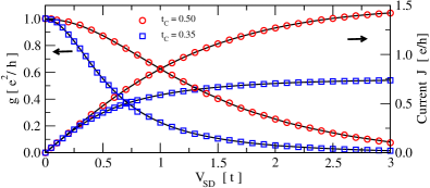
Our result for the conductance through a single impurity in Fig. 16 is in excellent quantitative agreement with exact diagonalization results already for moderate system sizes and DMRG cutoffs. Accurate calculations for extended systems with interactions are more difficult, mainly for two reasons: 1.) The numerical effort required for our approach depends crucially on the time to reach a quasi-stationary state. For the single impurity, the quasi-stationary state is reached on a timescale proportional to the inverse of the width of the conductance resonance, , in agreement with the result in Ref. Wingreen et al. (1993). In general, extended structures with interactions will take longer to reach a quasi-stationary state, and the time evolution has to be carried out to correspondingly longer times. 2.) In the adaptive td-DMRG, the truncation error grows exponentially due to the continued application of the wave function projection, and causes the sudden onset of an exponentially growing error in the calculated time evolution after some time. This ’runaway’ time is strongly dependent on the DMRG cutoff, and was first observed in an adaptive td-DMRG study of spin transport by Gobert et al.Gobert et al. (2005). To avoid these problems we resort to the full td-DMRG Schmitteckert (2004), which does not suffer from the runaway error.
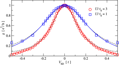
In Fig. 17 we show results for the first differential conductance peak of an interacting 7-site nanostructure. Careful analysis of the data shows, that in order to reproduce the line shape accurately, one has to introduce an energy dependent self energy for . Since the effect is small, we approximate it by a correction quadratic in the bias voltage difference . It is important to note that for the strongly interacting nanostructure, , the conductance peaks are very well separated. Therefore the line shape does not overlap with the neighboring peaks, and the fit is very robust. Performing the same analysis for a non-interacting nanostructure with a comparable resonance width, we obtain negligible corrections to in the self energy, indicating that the change of the line shape is due to correlation effects.
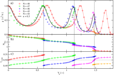
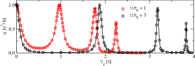
The linear conductance as a function of applied gate potential can be calculated in the same manner, if a sufficiently small external potential is used. We study the same 7-site nanostructure as before, with interaction , and use a bias voltage of . For half filled leads, the result for the linear conductance calculated with a fixed number of fermions, , is qualitatively correct, but the conductance peaks are shifted to higher energies relative to the expected peak positions at the energy levels of the non-interacting system (Fig. 18). Varying the gate potential increases the charge on the nanostructure by unity whenever an energy level of the nanostructure moves through the Fermi level [Fig. 18 (b)]. The density in the leads varies accordingly [Fig. 18 (c)]. Since the number of fermions in the system is restricted to integer values, direct calculation of the linear conductance at constant is not possible and one must resort to interpolation. Using linear interpolation in for yields our final result for the linear conductance at half filling [Fig. 18 (a)]. The agreement in the peak positions is well within the expected accuracy for a 96 site calculation. Our results for the conductance through an interacting extended nanostructure are presented in Fig. 19. The calculation for the weakly interacting system requires roughly the same numerical effort as the non-interacting system. In the strongly interacting case, where the nanostructure is now in the charge density wave regime, the time to reach a quasi-stationary state is longer, and a correspondingly larger system size was used in the calculation. In both cases we obtain peak heights for the central and first conductance resonance to within 1% of the conductance for a single channel.
VII Exponential damping
In this section we want to study the effect and possible applications of damped boundary conditions (DBC). DBC have been introduced Vekić and White (1993); Bohr et al. (2006) in order to reduce finite size effects. Here we would like to reduce the limitations rising from the finite transit time and the Josephson wiggling which especially in the low voltage regime and with an applied gate voltage spoils the accuracy of current measurements. We have already seen how to profit from the voltage dependency of the finite size wiggling by using a fit procedure which allows for the calculation of current–voltage characteristics even with an applied gate voltage. We now want to discuss the possibility of combining the fit procedure with DBC, where the damping effectively increases the system size. Furthermore we want to use DBC to adjust the single particle energy levels in order to increase the resolution with respect to when , cf. Fig. 15.
VII.1 Estimate for Transit Time in a system with half filling
In Fig. 20 we show the time dependent current through a single impurity with , including the initial transient regime as well as the finite size reflections for different values of the bias voltage . We compare two different system sizes with and lattice sites, and also apply exponentially DBC in order to demonstrate the effectively increased system size. The hopping matrix element is damped towards the boundaries of the system using a damping constant as sketched in Fig. 2, over a range of lattice sites. The total number of lattice sites is left unchanged (here: ). We find an enhanced size of the current plateaus, however, the damping can also lead to an early breakdown of the current.
As an estimate for the transit time of a wave packet traveling in undamped leads of size one can use the Fermi velocity which leads to
| (14) |
Assuming a local Fermi velocity in damped leads with damping leads to an expression of the form
| (15) |
where is the size of the damped leads. Eq. (15) can then be used to estimate an effective system size
| (16) |
This is in agreement with the results for the pseudo-steady current found for the noninteracting case, Fig. 20. For a more quantitative check of the formula we compare the transit time, extracted from a current measurement, to the estimate given by Eq. (15) [Fig. 21]. We therefore use two different criteria: (a) the time where becomes negative at the end of the first plateau (crosses), and (b) the time where the current changes sign after one round trip (squares). The black dotted lines show and for the undamped case. For values of close to we find that the estimate is well fulfilled over a wide range of values of for both (a) and (b) even for big bias voltage. The slight growth of is assumed to be caused by the different Fermi velocity of excitations for . However, the estimate tends to be totally wrong even for small bias voltage and small values of if becomes too small. The small plots at the top show the relative single particle level density. As expected, cf. Fig. 22, the level density grows with until a maximum is reached where the position of the maximum is determined by the bias voltage. It can clearly be seen that the position of the maximum in combination with the values of gives a strong indication if a current plateau is still well defined for a time scale given by the estimate of , since for values of on the left side of the maximum of the single particle level density. In comparison, (b) is a weak criterion since for strong damping the current plateau starts decaying for times much smaller than , cf. Fig. 20. In Fig. 22, we show the single particle energy levels of a system with lattice sites with a single impurity, as function of the damping constant as well as function of the size of the damped leads . The plot demonstrates the growth of the level density on the scale which in conjunction with Fig. 21 allows for an estimate of the maximum value of up to which a current plateau can be expected in a system with DBC.
VII.2 Fit Procedure
As already mentioned in Sec. V, the fitting procedure gets unreliable when the oscillation time substantially exceeds the time range . We therefore now want to demonstrate how to use the estimate for the transit time in order to implement damping conditions to sufficiently increase the effective system size, enforcing . As an example, we simulate the time evolution of a system with lattice sites and a single, non-interacting impurity with , and apply a small bias voltage . An effective transit time can be obtained using DBC, according to Eqns. (15, 16).
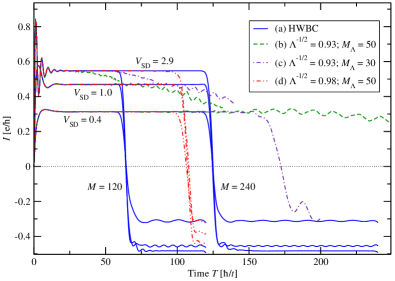
The result is presented in Fig. 23, where we show the time dependent current through one of the contact links of a single impurity for different damping conditions and two different values of . Again, we fit to the oscillating part of current expectation value. The extracted current for the calculations including DBC fits with the analytic result with an accuracy of which is of the same order of magnitude as compared to the mean value of the very small plateau regime that can be found for the system with HWBC. This leads us to the conclusion, that DBC can be used to obtain a first guess while for high precision measurements, HWBC with an increased system size have to be implemented.
VII.3 Correction of the single particle energy levels using DBC
In Section V.2 we found that the effects resulting from a finite density shift in the leads when applying a gate voltage can be significantly suppressed when extracting the current only for certain values of determined by the single particle level spacing. Since these finite size effects particularly arise in the middle of the band where the density of single particle levels is the lowest – and where the current has to be extracted for the calculation of the linear conductance – one would like to shift the levels towards the center of the band somehow. This can be achieved by increasing the number of lattice sites which also increases the numerical effort.
Applying DBC also results in a shift of the single particle energy levels in the leads towards the center of the band, cf. Fig. 22. We therefore state the question if the criterion formulated in Sec. V.2 still holds true for DBC. The result is shown in Fig. 15. To obtain the additional data points (b) we used damping conditions with values of and . We calculated the single particle energy levels for the decoupled leads and then obtained the current for values of the bias voltage with in the middle of two neighboring energy levels. To increase the resolution for the high voltage regime only moderate damping conditions are required (, ), while strong damping is imposed to get high resolution in the low voltage regime. For approaching the band edge, however, DBC have to be avoided for the reasons discussed above.
VIII Conclusions
We have reviewed the concept of extracting the finite bias and linear conductance from real time evolution calculations in finite systems. Very accurate quantitative results are possible, as long as finite size effects are taken into account. Our results for the linear conductance compare favorably both in accuracy and computational effort with the DMRG evaluation of the Kubo formula Bohr et al. (2006). Calculations of strongly interacting systems show correlation induced corrections to the resonance line shape.
Acknowledgements.
We profited from many discussions with Ferdinand Evers, Ralph Werner, and Peter Wölfle. We would like to thank Miguel A. Cazalilla for clarifying discussions. The authors acknowledge the support from the DFG through project B2.10 of the Center for Functional Nanostructures, and from the Landesstiftung Baden-Württemberg under project 710.References
- Sohn et al. (1997) L. L. Sohn, L. P. Kouwenhoven, and G. Schön, eds., Mesoscopic electron transport: Proceedings of the NATO Advanced Study Institute (1997).
- Landauer (1957) R. Landauer, J. Res. Dev. 1, 233 (1957).
- Landauer (1970) R. Landauer, Phil. Mag. 57, 863 (1970).
- Büttiker (1986) M. Büttiker, Phys. Rev. Lett. 57, 1761 (1986).
- Molina et al. (2004) R. A. Molina, P. Schmitteckert, D. Weinmann, R. A. Jalabert, G.-L. Ingold, and J.-L. Pichard, Eur. Phys. Jour. B 39, 107 (2004).
- Sushkov (2001) O. P. Sushkov, Phys. Rev. B 64, 155319 (2001).
- Molina et al. (2003) R. A. Molina, D. Weinmann, R. A. Jalabert, pers/G.-L. Ingold, and J.-L. Pichard, Phys. Rev. B 67, 235306 (2003).
- Meden and Schollwöck (2003) V. Meden and U. Schollwöck, Phys. Rev. B 67, 193303 (2003).
- Freyn et al. (2009) A. Freyn, G. Vasseur, P. Schmitteckert, D. Weinmann, G.-L. Ingold, R. A. Jalabert, and J.-L. Pichard (2009), eprint arXiv:0909.5048.
- Oguri et al. (2005) A. Oguri, Y. Nisikawa, and A. C. Hewson, .Phys. Soc. Jpn. 74, 2554 (2005).
- Meir et al. (1991) Y. Meir, N. S. Wingreen, and P. A. Lee, Phys. Rev. Lett 66, 3048 (1991).
- Louis and Gros (2003) K. Louis and C. Gros, Phys. Rev. B 68, 184424 (2003).
- Bohr et al. (2006) D. Bohr, P. Schmitteckert, and P. Wölfle, Europhys. Lett. 73, 246 (2006).
- Bohr and Schmitteckert (2007) D. Bohr and P. Schmitteckert, Phys. Rev. B 75, 241103(R) (2007).
- Schmitteckert and Evers (2008) P. Schmitteckert and F. Evers, Phys. Rev. Lett. 100, 086401 (2008).
- Karrasch et al. (2006) C. Karrasch, T. Enss, and V. Meden, Phys. Rev. B 73, 235337 (2006).
- Büsser et al. (2000) C. A. Büsser, E. V. Anda, A. L. Lima, M. A. Davidovich, and G. Chiappe, Phys. Rev. B 62, 9907 (2000).
- Meir and Wingreen (1992) Y. Meir and N. S. Wingreen, Phys. Rev. Lett 68, 2512 (1992).
- Schoeller and König (2000) H. Schoeller and J. König, Phys. Rev. Lett. 84, 3686 (2000).
- Stefanucci and Almbladh (2004a) G. Stefanucci and C.-O. Almbladh, Europhys. Lett. 67, 14 (2004a).
- Stefanucci and Almbladh (2004b) G. Stefanucci and C.-O. Almbladh, Phys. Rev. B 69, 195318 (2004b).
- Di Ventra and Todorov (2004) M. Di Ventra and T. N. Todorov, J. Phys.: Condens. Matter 16, 8025 (2004).
- Bushong et al. (2005) N. Bushong, N. Sai, and M. Di Ventra, Nano Letters 5, 2569 (2005).
- Weiss et al. (2008) S. Weiss, J. Eckel, M. Thorwart, and R. Egger, Phys. Rev. B 77, 195316 (2008).
- Han and Heary (2007) J. E. Han and R. J. Heary, Phys. Rev. Lett. 99, 236808 (2007).
- Cazalilla and Marston (2002) M. A. Cazalilla and J. B. Marston, Phys. Rev. Lett. 88, 256403 (2002).
- Luo et al. (2003) H. G. Luo, T. Xiang, and X. Q. Wang, Phys. Rev. Lett. 91, 049701 (2003).
- Daley et al. (2004) A. J. Daley, C. Kollath, U. Schollwöck, and G. Vidal, J. Stat. Mech.: Theor. Exp. p. P04005 (2004).
- White and Feiguin (2004) S. R. White and A. E. Feiguin, Phys. Rev. Lett. 93, 076401 (2004).
- Schmitteckert (2004) P. Schmitteckert, Phys. Rev. B 70, 121302(R) (2004).
- Feiguin and White (2005) A. E. Feiguin and S. R. White, Phys. Rev. B 72, 020404(R) (2005).
- Al-Hassanieh et al. (2006) K. A. Al-Hassanieh, A. E. Feiguin, J. A. Riera, C. A. Büsser, and E. Dagotto, Physical Review B (Condensed Matter and Materials Physics) 73, 195304 (pages 11) (2006).
- Boulat et al. (2008) E. Boulat, H. Saleur, and P. Schmitteckert, Physical Review Letters 101, 140601 (pages 4) (2008).
- Heidrich-Meisner et al. (2009a) F. Heidrich-Meisner, A. E. Feiguin, and E. Dagotto (2009a), eprint cond-mat/0903.2414.
- Heidrich-Meisner et al. (2009b) F. Heidrich-Meisner, G. B. Martins, C. A. Büsser, K. A. Al-Hassanieh, A. E. Feiguin, G. Chiappe, E. V. Anda, and E. Dagotto, Eur. Phys. J. B 67, 527 (2009b).
- Kirino et al. (2008) S. Kirino, T. Fujii, J. Zhao, and K. Ueda, Journal of the Physical Society of Japan 77, 084704 (2008).
- da Silva et al. (2008) L. G. G. V. D. da Silva, F. Heidrich-Meisner, A. E. Feiguin, C. A. Büsser, G. B. Martins, E. V. Anda, and E. Dagotto, Physical Review B (Condensed Matter and Materials Physics) 78, 195317 (pages 9) (2008).
- Schmitteckert (2007) P. Schmitteckert, in High Performance Computing in Science and Engineering ’07, edited by W. E. Nagel, D. B. Kröner, and M. Resch (Springer, Berlin, 2007), pp. 99–106.
- Ulbricht and Schmitteckert (2008) T. Ulbricht and P. Schmitteckert, in High Performance Computing in Science and Engineering ’08, edited by W. E. Nagel, D. B. Kröner, and M. Resch (Springer, Berlin, 2008), pp. 71–82, ISBN 978-3-540-88301-2.
- Schneider and Schmitteckert (2006) G. Schneider and P. Schmitteckert (2006), eprint cond-mat/0601389.
- Branschädel et al. (2009) A. Branschädel, T. Ulbricht, and P. Schmitteckert, in High Performance Computing in Science and Engineering ’09, edited by W. E. Nagel, D. B. Kröner, and M. Resch (Springer, Berlin, 2009), p. 123, ISBN 978-3-642-04664-3.
- White (1992) S. R. White, Phys. Rev. Lett. 69, 2863 (1992).
- White (1993) S. R. White, Phys. Rev. B 48, 10345 (1993).
- Noack and Manmana (2005) R. M. Noack and S. R. Manmana, in LECTURES ON THE PHYSICS OF HIGHLY CORRELATED ELECTRON SYSTEMS IX: Ninth Training Course in the Physics of Correlated Electron Systems and High-Tc Superconductors, edited by A. Avella and F. Mancini (AIP, Salerno, Italy, 2005), vol. 789, pp. 93–163.
- Hallberg (2006) K. A. Hallberg, Adv. Phys. 55, 477 (2006).
- Schollwöck (2005) U. Schollwöck, Rev. Mod. Phys. 77 (2005).
- White (1996) S. R. White, Phys. Rev. Lett 77, 3633 (1996).
- Schmitteckert and Schneider (2006) P. Schmitteckert and G. Schneider, in High Performance Computing in Science and Engineering ’06, edited by W. E. Nagel, W. Jäger, and M. Resch (Springer, Berlin, 2006), pp. 113–126.
- Wingreen et al. (1993) N. S. Wingreen, A. P. Jauho, and Y. Meir, Phys. Rev. B 48, 8487 (1993).
- Cini (1980) M. Cini, Phys. Rev. B 22, 5887 (1980).
- Bâldea and Köppel (2010) I. Bâldea and H. Köppel (2010), eprint cond-mat/1002.4966.
- Mahan (2000) G. D. Mahan, Many particle physics (Kluwer Academics / Plenum Publishers, New York, 2000), 3rd ed., ISBN 0-306-46338-5.
- Gobert et al. (2005) D. Gobert, C. Kollath, U. Schollwöck, and G. Schütz, Phys. Rev. E 71, 036102 (2005).
- Vekić and White (1993) M. Vekić and S. R. White, Phys. Rev. Lett. 71, 4283 (1993).