Theory of oscillations in the STM conductance resulting from
subsurface defects
(Review Article)
Abstract
In this review we present recent theoretical results concerning investigations of single subsurface defects by means of a scanning tunneling microscope (STM). These investigations are based on the effect of quantum interference between the electron partial waves that are directly transmitted through the contact and the partial waves scattered by the defect. In particular, we have shown the possibility imaging the defect position below a metal surface by means of STM. Different types of subsurface defects have been discussed: point-like magnetic and non-magnetic defects, magnetic clusters in a nonmagnetic host metal, and non-magnetic defects in a -wave superconductor. The effect of Fermi surface anisotropy has been analyzed. Also, results of investigations of the effect of a strong magnetic field to the STM conductance of a tunnel point contact in the presence of a single defect has been presented.
pacs:
61.72.J Point defects and the defect clusters, 73.40.Cg Contact resistance, contact potential, 73.63.Rt Nanoscale contact, 74.50.+v Tunneling phenomena: single particle tunneling and STM, 73.23.-b Electronic transport in mesoscopic systems,72.10.Fk Scattering by point defects, dislocations, surfaces, and other imperfections (including Kondo effect)I Introduction
About three decades following its invention Binnig , scanning tunnelling microscopy (STM) has proved to be a superbly valuable tool for investigating surfaces on the atomic scale. Along with a mapping of the conductor’s surface, the STM enables observing many phenomena, among which electron scattering by single surface defects (impurity atoms, adatoms, or step edges). There are hundreds of papers that are devoted to investigations of surface defects by STM. In this paper we do not aim to review all of them and confine ourselves to briefly mentioning the main directions of researches in this field. Our attention will be mainly focused on interference effects in STM conductance caused by defects sitting below the surface.
Electron scattering by defects leads to quantum-interference patterns in the local electron density of states around the defects (Friedel oscillations Friedel ). For more than thirty years Friedel oscillations have remained a theoretical prediction that could be seen only in theory textbooks Ziman . The appearance of the STM has enabled the visualization of these oscillations, which manifest themselves as oscillations of the differential tunneling conductance, , around defects on the surface.
First standing wavelike patterns in the STM conductance in the vicinity of defects were observed by Crommie et al. Crommie on a Cu(111) surface and by Hasegava et al. Hasegava on a Au(111) surface. At the (111) surface of the noble metals Cu, Ag, and Au the electrons of the surface states form a quasi-two-dimensional nearly-free electron gas having an isotropic dispersion law Burgi . When scattered from step edges or adatoms the surface states form standing waves which result in an oscillatory dependence of the tunneling conductance measured as a function of the distance between the STM tip and the defect, . The period of the conductance oscillations is set by twice the Fermi wave vector, ( is a two-dimensional vector in the plane of the surface).
The circular 2D Fermi contour of the electrons at the (111) surface of noble metals results from the fact that the layer of surface atoms actually corresponds to one of the close-packed stackings on which the face-centered cubic structure is based. Generally, for less closely packed surfaces and conductors having a complicated crystallographic structure a 2D Fermi contour is anisotropic, i.e. the absolute value of the vector depends on its direction. The Fourier transform (FT) of the standing wave pattern provides an image of the Fermi contour. Anisotropic Friedel-like oscillations have been observed by FT-STM on Cu(110) surfaces Petersen2 , Be Sprunger , and ErSi2 Vonau . Particularly, in Ref. Petersen2 the contour related to the ’neck’ of the bulk Fermi surface for Cu (110) surface has been imaged.
Magnetic adatoms on non-magnetic host metal surfaces are of special interest as they produce a characteristic many-body resonance structure in the differential conductance near zero voltage bias attributed to the Kondo effect chen99 ; madhavan98 ; li98 ; knorr02 . The shape of the resonance in the differential conductance is usually asymmetric and is described by a Fano line shape fano61 ; plihal01 ; wahl04 . The surface electron waves carry information on the magnetic impurity and by focussing the waves it has been possible to create a mirage image of the impurity manoharan00 (for review, see corral ). The interesting phenomenon of an orbital Kondo resonance was observed by STM in Ref.Koles . It was found that STM images of the Cr(001) surface show cross-like depressions centered around the impurities corresponding to the orbital symmetry of two degenerate surface states Koles .
The investigation of defects near the surface of unconventional superconductors by STM is a way to determine the symmetry of the order parameter. The effect of single Zn defects on the superconductivity in high-Tc superconductors was investigated in Ref. Zn , and the manifestation of d-wave pairing symmetry was observed in the quasibound state near the defect. In Ref. MagImp a bound state near a magnetic Mn adatom on the surface of superconducting Nb was observed by STM.
An effective way to enhance the STM sensitivity to such oscillation effects is to use a superconducting tip Pan . In Ref. Xu it was demonstrated that the amplitude of conductance oscillations is significantly enhanced when a superconducting tip is used, and when the applied bias is close to the gap energy of the superconductor.
The applicability of STM can be extended to the study of magnetic objects on the surface of a conductor when a magnetic material is used for the STM tip such that the electric current is spin polarized (SP) (for review of SP-STM see Bode ). For example, the precession of a magnetic moment of clusters of organic molecules on a surface gives rise to a time modulation of the SP-STM current, from which the - factor can be found Manoharan ; Durkan . The possibility to probe magnetic properties of nanostructures buried beneath a metallic surface by means of local probe techniques is discussed in Ref.Brovko . It has been shown that those properties can be deduced from the spin-resolved local density of states above the surface Brovko .
STM spectroscopy also provides access to information on the structure of the metal below the surface in both semiconductors and metals. Crampin Crampin proposed to utilize the surface states for imaging subsurface impurities. However, the exponential decay of the wave function amplitude into the bulk limits the effective range to the topmost layers only and bulk states form a good alternative for detecting defect positions. The principle of imaging subsurface defects is based on the influence on the conductance caused by quantum interference of electron waves that are scattered by defects and reflected back by the contact. This effect was explored for investigating subsurface Ar bubbles submerged in Al Schmid and Cu Kurnosikov , and Si(111) step edges buried under a thin film of Pb Hongbin . In these experiments, bulk electrons are found to be confined in a vertical quantum well between the surface and the top plane of the object of interest. The observation of interference patterns due to electron scattering by Co impurities in the interior of a Cu sample was reported Refs. Quaas ; Weismann .
Reviews of STM theory can be found in Refs. Hofer ; Blanco . The papers listed in Hofer ; Blanco , in which the conductance of a tunnel contact of small size has been analyzed theoretically, must be complemented by reference to the fundamental paper of Kulik, Mitsai and Omelyanchouk KMO published in 1974. In this paper the authors obtained, on the basis of rigorous quantum-mechanical considerations, an analytical formula for the conductance of a junction between two metal half-spaces separated by an inhomogeneous tunnel barrier of low transparency. Their result is valid for arbitrary values of the applied bias and for arbitrary dependence of the tunnelling probability on the coordinates in the plane of the interface between the metals. As a special case, the general formula for the contact resistance can be applied to an inhomogeneous tunnel contacts having a characteristic diameter smaller than electron wave length, which is suitable to describe STM conductance. Recently, electron tunnelling through a randomly inhomogeneous barrier of arbitrary amplitude has been analyzed theoretically in Refs. Bezak1 ; Bezak2 .
The theoretical descriptions of STM conductance oscillations due to electron scattering by single defects in the majority of papers is based on the assumption that the tunnelling conductance measured by the STM tip is proportional to the local density of states (LDOS) of the sample (see, for example, Crampin ; corral ; Balatsky ; Stepanyuk ) as for a planar tunnel junction Wolf . For the scattering of electron surface states this assumption is quite reasonable, but for electron scattering in the bulk of the sample it can not be used. The LDOS in the vicinity of defects in the bulk is critically modified by electron reflections off the surface of the conductor, at , and differs from Friedel oscillations of the LDOS in an infinite conductor with a single scatterer Ziman . In the limit of zero tunnelling probability we have Further, the conductance oscillations are formed only by ”tagged” electrons, which tunnel through the contact and are scattered back by the defect, while a ”halo” of Friedel oscillations around the defect is due to all scattered electrons. In general, there are no other periods in the interference effects but the period of Friedel oscillations ( is a Fermi wave vector) and the analysis in Ref. Weismann of the experimental data in terms of a bulk LDOS seems to be qualitatively correct Kobayashi . However, the calculation of amplitudes and phases of the conductance oscillations, which contain additional information on the interaction of the charge carriers with the defect, requires the solution of the scattering problem of the influence of subsurface defects on the conductance of a small tunnel contact.
In this paper we review a series of publications in which the theory of the electronic transport though a tunnel point-contact in the presence of a single defect below metal surface was developed. The organization of this paper is as follows. The model of the tunnel contact and the basic equations that describe the effect of subsurface defects on the STM conductance are presented in Sec. II. The solution of the Schrödinger equation for elections that tunnel through the contact and are scattered by the defect is given. In Sec. III a method to determine the defect positions below a metal surface is formulated on the basis of an investigation of the nonlinear conductance of the contact. A signature of the Fermi surface anisotropy in STM conductance in the presence of subsurface defects is discussed in Sec. IV. In Sec. V we present the results of investigations of the effect of a subsurface magnetic defect on the tunnel current, including the signature of a Kondo impurity and that of a magnetic cluster having an unscreened magnetic moment. In Sec. VI it is shown that a strong magnetic field leads to specific magneto-quantum oscillation periods which depend on the distance between the contact and the defect. The possibilities of studying the interference of quasiparticles in a superconductor is analyzed in Sec. VII. In Sec. VIII we conclude by discussing the possibilities for exploiting these theoretical results for sub-surface imaging along with experimental investigations of physical characteristics of subsurface defects.
II Quantum interference of scattered electron waves in the vicinity of a point contact
II.1 Model of a STM contact, and the Schrödinger equation for the system
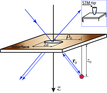
As a model for the STM experiments we choose an inhomogeneous tunnel contact between two metal half-spaces separated by an infinitely thin interface. The potential barrier in the plane of the interface, at , is taken to be described by a delta function KMO ,
| (1) |
where is the radius vector in the plane of the interface, perpendicular to the axis. The function at all points of the plane except for a small region defining the contact, having a characteristic radius , at which is of order 1. As an example, a suitable model for the function for the ”STM tip” is the Gaussian function with small Another useful model of the junction is an orifice of radius for which for in the plane of the contact (Fig. 1).
Of course, such a model describes only the qualitative features of the conductance of an STM contact, and does not contain such parameters as the tip radius, or the distance between the STM tip and the sample as is represented, for example, in the model by Tersoff and Hamann Tersoff . In principle these properties of the system may be included in the model as parameters of the function The advantage of the model by Kulik et al. KMO is the possibility of finding exact analytical solutions of the Schrödinger equation in the limit . The equations are considerably simplified in the case of a small contact The wave functions obtained in the framework of the model barrier (1) properly describe the spreading of electron waves into the bulk metal from a small region on its surface. A numerical value for the STM conductance plays the role of a scale factor for the conductance oscillations, and for the further considerations below it is of less importance.
A defect in the vicinity of the interface can be described by the potential
| (2) |
where is the constant of the electron interaction with the defect, and is a spherically symmetric function localized within a region of characteristic radius centered at the point , which satisfies the normalization condition
| (3) |
The electron wave function in a metal with a dispersion relation must be found from the Schrödinger equation LAK
| (4) |
Here is the vector-potential of the stationary magnetic field , and is the applied electrical potential, corresponds to different spin directions, is the Bohr magneton, where is the free electron mass, and is the electron -factor. The function satisfies at the following boundary condition for continuity of the wave function
| (5) |
and the condition, which for a function barrier is obtained by the integration of the Schrödinger equation (4) over an infinitesimal interval near the point
| (6) |
In this section below we consider a solution of Schrödinger equation (4) for a free electron model with an electron effective mass and a dispersion relation in the absence of external fields ( ). In this case the condition (6) reduces to the well-known condition for the jump of the derivative of the wave function
| (7) |
The effects of applied voltage, Fermi surface anisotropy and magnetic field are discussed in next sections.
II.2 Wave function due to an inhomogeneous tunnel barrier
Here we follow the procedure for the finding the electron wave function in the limit that was proposed in Ref. KMO . To first approximation in the small parameter the wave function can be written as:
| (8) |
where is of order This latter part of the wave function (8) describes the electron tunnelling through the barrier and determines the electrical current. The first term in the Eq.(8) is the solution of the Schrödinger equation for the metallic half-spaces without the contact
| (9) |
where and are the components of the wave vector parallel and perpendicular to the interface, respectively. The expression (9) satisfies the boundary condition at the interface.
Substituting the wave function (8) into the boundary conditions (5)and (6) one must match terms of the same order in As a result the conditions (5), (6) are reduced to KMO
| (10) |
| (11) |
where
| (12) |
is the amplitude of the electron wave function passing through the homogeneous barrier. Developing the function as a Fourier integral in the coordinate , and using the Eq. (11), we find KMO
| (13) |
where For a homogeneous -function barrier, , Eq. (13) transforms into a transmitted plane wave having an amplitude .
The characteristic radius of the region on the surface through which electrons tunnel from the STM tip into the sample is of atomic size, , while the Fermi wave vector Å By using the condition after integrating over and in Eq.(13) we find Avotina08mi
| (14) |
The incident plane wave is transformed into a spherical p-wave (14) after scattering by the point contact. In Eq. (14), and below, are the spherical Hankel functions. Note that the wave function (14) is zero in all points on the surface , except the point (at the contact) where it diverges. This divergence is the result of taking the limit in the integral expressions for (13). Yet, Eq. (14) gives a finite value for the total charge current through the contact as obtained by integration over a half-sphere of radius with its center in the point for .
II.3 Electron scattering by a single defect in the vicinity of a tunnel point contact
As a result of current spreading only a small region near the point contact noticeably influences the conductance. For high purity samples only a few defects will be found in this region. At low temperatures the distance between the contact and the nearest defect, , is smaller than the electron mean free path due to electron-phonon scattering and the electrons are elastically scattered by the single defect only. The wave function of transmitted electrons, , which takes into account the scattering by the defect, can be expressed in terms of the retarded Green function of the homogeneous equation (4) at , in absence of impurity scattering. To first approximation in the transmission amplitude (12) the integral equation for is given by
| (15) |
where
| (16) |
is the electron Green’s function of Eq. (4) for the semi-infinite half-space , and is given by Eq. (13). For small Eq. (15) can be solved by perturbation theory, i.e. in first approximation in the function in the integral term should be replaced by
For a short range potential ( ) the function can be taken outside of integral in Eq. (15) and the scattered wave function is written as Grenot
| (17) |
where
| (18) |
Note that Eq.(17) is valid far from the defect () and the function must provide the convergence for the integral in the denominator of Eq. (18) at . As is well known, s-wave scattering is dominant for scattering by a short range potential and the scattering matrix (18) can be expressed by the s-wave phase shift Avotina08mi
| (19) |
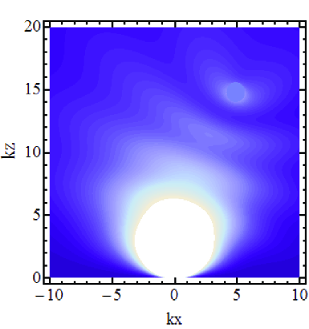
The effective -matrix is an oscillatory function of the distance between the defect and the interface that results from repeated electron scattering by the defect after its reflections from the interface. Figure 2 illustrates the spatial distribution of the square modulus of the wave function (17) in the vicinity of the contact with the defect placed at
III Friedel-like oscillations of the tunnel point contact conductance
III.1 Voltage dependence of the STM conductance
In the case of a small transparency (12) the applied voltage drops entirely over the barrier and the electrical potential can be chosen as a step function At zero temperature electrons tunnel to the lower half-space when , and for electrons can tunnel only to available states in the upper half-space (Fig. 1).
The tunnelling current is the difference between two currents flowing through the contact in opposite directions. Each of them can be evaluated by means of the probability current density integrated over a plane , and integrating over all directions of the electron wave vector
| (20) |
where is the electron density of states for one spin direction, denotes the average over an iso-energy surface ,
| (21) |
is an element of the iso-energy surface in -space, and is the velocity operator. For a free-electron model of the energy spectrum A voltage dependence of the current density (20) is defined by the dependence of the absolute value of the wave vector for the incident on the contact electron .
The total current through the contact is
| (22) |
where is the Fermi function.
The current-voltage characteristics is calculated by substituting wave function (17) into Eq. (22) and taking into account Eqs. (13) and (16). Retaining only terms to first order in (i.e. ignoring multiple scattering at the impurity site, in Eq. (17) ), and in the limit of low temperatures, , the conductance can be written as Avotina05
| (23) | |||
where
| (24) |
and and are the spherical Bessel functions, and
| (25) |
is the Fermi wave vector accelerated by the potential difference. In Eq.(23) for definiteness a positive sign of the bias is chosen, .
If the contact radius ( is the Fermi wave length), the expression for the conductance (23) can be simplified
| (26) |
where
| (27) |
is the inherent conductance of the tunnel point contact, ,
| (28) |
| (29) |
| (30) |
and
| (31) |
is the dimensionless constant of interaction.
Equation (26) describes the oscillations of the STM conductance as a function of the distance between the STM tip and the subsurface defect, and as a function of the bias . For distances between the contact and the defect and the oscillatory dependence becomes sinusoidal
| (32) |
Oscillations of the STM conductance as a function of the voltage, due to the quantum interference caused by impurity scattering, were observed by Untiedt et al. Untiedt , and Ludoph et al. Ludoph .
III.2 Determination of the defect positions
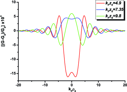
Now we proceed to discuss whether this effect can be exploited experimentally for three dimensional mapping of subsurface impurities. The position of the defect in the plane parallel to the surface can be found from an analysis of oscillatory pattern in the dependence In the majority of cases the center of this pattern corresponds to the tip position directly above the defect, A possible effect of the Fermi surface anisotropy is discussed in the next section. Note that, in contrast to the case of surface defects, the oscillations in the conductance (26) are not periodic in the tip distance along the surface, but their period is defined by the distance . Generally, the depth may be found by fitting the experimental data to the theoretical dependence (26). Figure 3 illustrates the oscillatory component of as a function of for different choices of . In this plot we have used the values for the constant the Fermi wave vector Å-1 and the interatomic distance Å for Cu. Thus, the plots correspond to defect positions in the third, fourth, and fifth layers below the Cu surface. The dependencies closely resemble the observations by Quaas et al. Quaas for Co atoms embedded in Cu(111).
For the determination of the defect depth one may use the periodicity in phase of (32) at sufficiently large According to Eq. (32) at two sequential radii and , , corresponding to neighboring maxima (or minima) satisfy the obvious condition of periodicity, For known it is a simple algebraic equation for the solution of which is
| (33) |
Note that and the radicand is positive. A second possibility of changing the product is by varying the maximum value of the electron wave vector by the applied voltage.
A first approach for determining the defect depth from the bias dependence of the period of the Friedel-like oscillations of the STM conductance was described by Kobayashi Kobayashi . The depth can estimated by tracing the point while changing the bias voltage , keeping the phase of the oscillations constant: where and are the positions corresponding to two different bias voltages and but the same phase (for example, a fixed maximum) Kobayashi . The solution of mentioned above equation with (25) gives
| (34) |
where
The method proposed in Ref. Avotina05 has certain advantages. If the STM tip is placed above the defect () the conductance amplitude decreases with depth of the defect as , which gives hope to observe the defects at sufficiently large distances below the surface. The depth of an impurity may be derived from the curve at which shows oscillations in with period and
| (35) |
In a real experiment it is not necessary to observe a full period of and, for example, a quarter of the period will be sufficient for the determination of the defect depth Avotina05 .
IV Signature of the Fermi surface anisotropy
In most metals the dispersion relation for the charge carriers is a complicated anisotropic function of momentum. This leads to anisotropy of the various kinetic characteristics LAK . Particularly, as shown in Ref. Kosevich , the current spreading may be strongly anisotropic in the vicinity of a point-contact. This effect influences the way the point-contact conductance depends on the position of the defect. For example, in the case of a Au(111) surface the ‘necks’ in the Fermi surface (FS) should cause a defect to be invisible when probed exactly from above.
Qualitatively, the wave function of electrons injected by a point contact for arbitrary FS has been analyzed by A. Kosevich Kosevich . He noted that at large distances from the contact the electron wave function for a certain direction is defined by those points on the FS for which the electron group velocity is parallel to Unless the entire FS is convex there are several such points. The amplitude of the wave function depends on the Gaussian curvature in these points, which can be convex or concave . The parts of the FS having different signs of curvature are separated by lines of (inflection lines). In general there is a continuous set of electron wave vectors for which . The electron flux in the directions having zero Gaussian curvature exceeds the flux in other directions Kosevich .
Electron scattering by defects in metals with an arbitrary FS can be strongly anisotropic LAK . Generally, the wave function of the electrons scattered by the defect consists of several superimposed waves, which travel with different velocities. In the case of an open FS there are directions along which the electrons cannot move at all. Scattering events along those directions occur only if the electron is transferred to a different sheet of the FS LAK .
In this section we analyze the effect of anisotropy of the FS to the signals for determination of the position of a defect below a metal surface by use of a STM. We show below that the amplitude and the period of the conductance oscillations are defined by the local geometry of the FS, namely by those points for which the electron group velocity is directed along the radius vector from the contact to the defect. General results are illustrated for the FS of noble metals.
At first we do not specify the specific form of the dependence , except that it satisfies the general condition of point symmetry . In the reduced zone scheme a given vector identifies a single point within the first Brillouin zone. As for isotropic FS, the electron wave function in the metal with an arbitrary dispersion relation can be found at by using the method described in Sec.III. The boundary conditions for the transmitted wave function have the same form as Eqs. (10), (11) in which the function must be replaced by
| (36) |
For the model of free electrons Eq.(36) transforms into Eq.(12). The components of vector perpendicular to the interface for electrons incident on the contact, , and reflected from the contact, , are related by conditions of conservation of the energy and the tangential component of the wave vector
| (37) |
The wave function scattered by the defect is defined by the general relation (15).
General expressions for the STM conductance into a metal having an arbitrary FS one can find in Ref. Avotina06 . Here, we present simplified asymptotic expressions for the oscillatory part of the conductance (the difference between the total conductance and its value in the absence of the defect) which are valid for large distances between the contact and the defect , Avotina06 ,
| (38) | |||
All functions of the wave vector in Eq. (38) are taken at the points of the FS for which the electron group velocity is parallel to the vector , is the wave vector corresponding to the point on the FS, in which The function is well known in the differential geometry as the support function of the surface Aminov . If the curvature of the FS changes sign, there is more than one point () for which . It may also occur that for given directions of the vector for all points on the FS, and the electrons cannot propagate along these directions LAK . For such the oscillatory part of the conductance is zero.
In Eq. (38)
| (39) |
is defined by Eq. (21), in the point defined by the direction of the vector in -space, is the Gaussian curvature of the FS,
| (40) |
is the algebraic adjunct of the element of the inverse mass matrix .
The Eq.(38) is valid, if curvature For those points at which the amplitude of the electron wave function in a direction of zero Gaussian curvature is larger than for other directions. This results in an enhanced current flow near the cone surface defined by the condition Kosevich ; Avotina06 . If the FS is open, there are directions along which the electron flow is absent. These properties of the wave function manifest itself in an oscillatory part of the conductance (38): 1) The amplitude of oscillations is maximal if the direction from the contact to the defect corresponds to the electron velocity belonging to an inflection line. 2) There are no conductance oscillations, if this direction belong to cones, in which the electron motion is forbidden.
For an ellipsoidal FS the Schrödinger equation can, in fact, be solved exactly in the limit and the conductance of the contact can be found for arbitrary distances between the contact and the defect. For this FS the dependence of the electron energy on the wave vector is given by relation,
| (41) |
were are the components of the electron wave vector , are constants representing the components of the inverse effective mass tensor .
Accurate to within first order in (i.e. ignoring multiple scattering at the impurity site), the conductance in the limit Avotina06 is given by
| (42) |
where in Eq. (42) is the conductance in the absence of a defect Avotina06 :
| (43) |
| (44) |
is given by Eq. (29).
The center of the oscillation pattern in the conductance as the function of the tip position corresponds to with respect to the point contact at , where
| (45) |
The support function for such tip position,
| (46) |
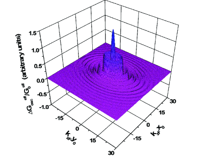
corresponds to the extremal value of the chord of the FS in the direction normal to the interface, is the unit vector in the direction of the vector . Figure 4 shows that is an oscillatory function of the defect position that reflects the ellipsoidal form of the FS and the oscillations are largest when the contact is placed in the position , defined by Eq. (45).
In deriving Eq. (38) it has been assumed that For finite voltage, but , all functions of the energy in Eq. (38) can be taken at , except in the oscillatory functions. When ,
| (47) |
and when the product clearly the conductance (38) is an oscillatory function of the voltage . The periods of the oscillations are defined by the energy dependence of the function . The results obtained properly describe the total conductance at and also can be used for the analysis of the periods of the oscillations at
Further calculations require information about the actual shape of the FS, In Ref. Avotina06 a model FS in the form of a corrugated cylinder was considered. Using this model, for which analytical dependencies of the conductance on defect position can be found, the manifestation of common features of FS geometries in the conductance oscillations was described: the anisotropy of convex parts (‘bellies’), the changing in sign of the curvature (inflection lines), and the presence of open directions (‘necks’).
In Ref. Avotina08nm a numerical analysis of the conductance oscillation pattern was made for the noble metals copper, silver and gold on the basis of Eq. (38). The parameterization of the FS was taken from FS ,
which is accurate up to 99%. The values for the constants are , , and is different for each metal. For copper, silver, and gold nm, nm, and nm, respectively. The Fermi energy of copper is 7.00eV, for silver 5.49eV and for gold it is 5.53eV.
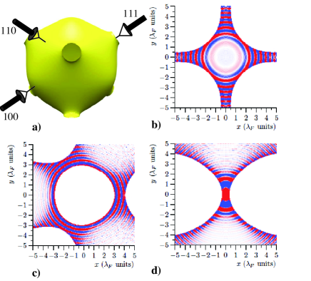
The results of computations for three crystallographic orientations are presented in Fig. 5. All distances in Fig. 5 are given in units of which for copper is 0.46nm, and for silver and gold it is 0.52nm. For each of the surface orientations the graphs have the symmetries of that particular orientation of the FS. In all figures ’dead’ regions can be seen, for which the conductance of the contact is equal to its value without the defect, showing no conductance oscillations. These regions originate from the ’necks’ of the FS and their edges are defined by the inflection lines. For all orientations of the metal surface the defect position in the plane of the surface corresponds to a center of symmetry. The appearance of ’dead’ regions depends on the depth of the defect, which can be estimated in the following way: The orientations of the ’neck’ axes define the axes of the cones with an opening angle , in which there are no scattered electrons. Vertexes of the cones coincide with the defect. The radius of the central ’dead’ region, is proportional to the depth of the defect Quaas .
The possibility of visualizing the Fermi surface of Cu in real space by investigation of interference patterns caused by subsurface Co atoms has been demonstrated by Weismann et al. Weismann .
V Subsurface magnetic defects
V.1 Kondo impurity
In the case of a magnetic defect at low temperatures (, where is the Kondo temperature) the Kondo resonance results in a dramatic enhancement of the effective electron-impurity interaction Abrikosov and perturbation methods become inapplicable. Kondo correlations give rise to a sharp resonance in the density of states at the energy near the Fermi level. For the effective electron scattering cross section acquires a maximum value corresponding to the Kondo phase shift Abrikosov . In this case, multiple scattering needs to be taken into account, even for a single defect, because of electron reflection by the metal surface.
In this subsection the conductance is expressed by means of a s-wave scattering phase shift . The results describe the influence to the conductance of multiple scattering of the electrons, which results in the appearance of harmonics in the dependencies of on the applied voltage, and on the distance between the contact and the defect. The analysis of the non-monotonic voltage dependence of the conductance is applied specifically to the interesting problem of Kondo scattering, using an appropriate phase shift Shift :
| (49) |
The first term in Eq. (49) describes the resonant scattering on a Kondo impurity level ( is the Kondo temperature). For a non-magnetic impurity this term is absent. The second term takes into account the usual potential scattering.
Taking Eq. (17) for the wave function of a spherical Fermi surface and Eq. (19) for the scattering matrix makes it possible to find the differential conductance, , of the tunnel point contact in the approximation of s-wave scattering. For and for is given by Avotina08mi
| (50) |
and for ,
| (51) |
Here is given by Eq. (27), and
| (52) | |||
is s-wave phase shift 49, and and are the spherical Bessel functions.
At low voltage the conductance can be expressed by an expansion in the small parameter ,
| (54) | |||
The second term in Eq. (54) gives the sum over scattering events by the defect and reflections by the surface. If we keep only the term for Eq. (54) reduces to the result obtained by perturbation theory in Sec. 3 above, which is valid for The arguments of the sine and cosine functions in Eq. (54) correspond to the phase that the electron accumulates while moving along semiclassical trajectories.
The voltage dependence of the conductance is not symmetric around . This asymmetry arises from the dependencies of the phase shift (49) and the absolute value of the wave vector on the sign of . The physical origin of this asymmetry comes from the fact that the scattering amplitude depends on the electron energy in the lower half-space (see Fig. 1), where the defect is situated. This energy is different for different directions of the current.
It is interesting to observe that the sign of the Kondo anomaly depends on the distance between the contact and the defect . This distance in combination with the value of the wave vector determines the period of oscillation of . If the bias coincides with a maximum in the oscillatory part of conductance the sign of the Kondo anomaly is positive and vice versa, a negative sign of the Kondo anomaly is found at a minimum in the periodic variation of
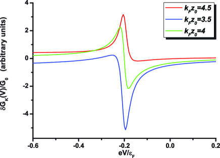
The Fig.6 shows the difference between voltage dependencies for a magnetic and a non-magnetic impurity, having the same potential scattering strength. The plots in Fig.6 demonstrate the evolution of the shape of the Kondo anomaly for several values of the distance between the contact and the impurity, placed on the contact axis. The change of distance changes the periodicity of the normal-scattering oscillations which leads to a changing of sign in the Kondo signal. A similar dependence of the differential conductance with the distance between an STM tip and an adatom on the surface of a metal has been obtained theoretically in Refs. Zawad ; Lin in terms of a Anderson impurity Hamiltonian Anderson . Note that we obtain a Fano-like shape of the Kondo resonance in the framework of a single-electron approximation Avotina08mi , while in Refs. Zawad ; Lin many-body effects were taken into account.
V.2 Magnetic cluster
In this subsection we consider the influence on the conductance of a tunnel point-contact between magnetic and non-magnetic metals of a defect having an unscreened magnetic moment, in a spin-polarized scanning tunnelling microscope (SP-STM) geometry Bode . A magnetic cluster is assumed to be embedded in a non-magnetic metal in the vicinity of the contact. As first predicted by Frenkel and Dorfman Frenkel particles of a ferromagnetic material are expected to organize into a single magnetic domain below a critical particle size (a typical value for this critical size for Co is about 35nm). Depending on the size and the material, the magnetic moments of such particles can be Vonsovsky .
Generally, the moment of the cluster in a non-magnetic metal is free to choose an arbitrary direction. This direction can be held fixed by an external magnetic field , the value of which is estimated as , where is the temperature (see, for example, Ref. Vonsovsky ). For and K the field is of the order of T. If is much larger than the magnetocrystalline anisotropy field of the magnetic STM tip, the direction of the external magnetic field controls the direction of the cluster magnetic moment but its influence on the spin-polarization of the tunnel current is negligible. In this case the magnetic moment of the cluster is ’frozen’ by the field and the problem becomes a stationary one.
If the external magnetic field is sufficiently weak and the radius of the electron trajectories is much larger than the distance between the contact and the cluster , the effects of modulation of the tunnel current due to electron spin precession Jedema and trajectory magnetic effects Avotina07 are negligible.
The geometry of a SP-STM experiment can be described in the framework of the model presented in Fig. 1, in which the half-space is taken up by a ferromagnetic conductor with magnetization . In Ref. Avotina09 the direction of the vector , which defines the direction of the polarization of tunnel current is chosen along the -axis. In real SP-STM the polarization of STM current is defined by the magnetization of the last atom of the tip Bode . A magnetization oriented along the contact axis can be obtained, for example, for a Fe/Gd-coated W STM tip Kub .
The interaction potential of the electrons with the cluster is a matrix consisting of two parts
| (55) |
where is the constant describing the non-magnetic part of the interaction (for the potential is repulsive), is the constant of exchange interaction, is the magnetic moment of the cluster, with the Pauli matrixes, and is the unit matrix. The function satisfies the condition (3). In the case of spin flip scattering the spinor electron wave functions satisfy the Schrödinger equation (4), in which the scattering potential must be replaced by the matrix (55). Under the assumptions that the potential and the transparency of the tunnel barrier in the contact plane are small the two-component wave function can be found by the method described in Sec. II.
The difference in absolute values of the wave vectors for spin-up and spin-down electrons (for the same energy ), which move towards the contact from the ferromagnetic bank,
| (56) |
results in different amplitudes (see Eq. (12)) of the electron waves injected into the non-magnetic metal for different directions of the spin ( is the electron g-factor). The total effective polarization of the current depends on the difference between the probabilities of tunnelling for different ,
| (57) |
The conductance of the contact at and is given by Avotina09
| (58) |
where is the conductance of the contact in absence of the cluster
| (59) |
is the absolute value of the Fermi wave vector in the magnetic metal for spin direction (see Eq. (56)), and
| (60) |
The function is defined by Eq. (29). When the radius of action of the function is much smaller than the distance between the contact and the center of the cluster, is an oscillatory function of for as for point defect with (see, Eq. (26) at ), but the oscillation amplitude is reduced as a result of superposition of waves scattered by different points of the cluster. The integral (60) can be calculated asymptotically for and For a homogeneous spherical potential ( is the cluster volume) the function takes the form
| (61) |
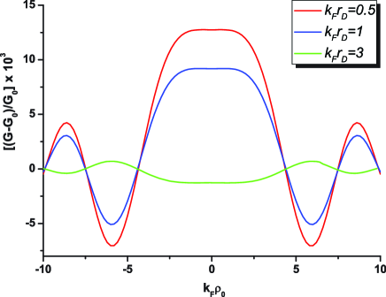
where is the cluster diameter. The last factor in Eq. (61) describes the quantum size effect related with electron reflections by the cluster boundary. Such oscillations may exist, if the cluster boundary is sharp on the scale of the electron wave length. Fig. 7 shows the dependence of the amplitude of the conductance oscillations on the cluster diameter. It demonstrates that a -phase shift may occur resulting from interference of electron waves over a distance of the cluster diameter.
In Eq. (58) the term proportional to takes into account the difference in the probabilities of scattering of electrons with different by the localized magnetic moment It depends on the angle between the tip magnetization and , as The same dependence was first predicted for a tunnel junction between ferromagnets for which the magnetization vectors are misaligned by an angle Slonczewski , and this was observed in SP-STM experiments Bode .
Note that once the spin-polarized current-induced torque pulls the magnetic moment away from alignment with , the cluster moment will start precessing around the field axis. The Larmor frequency is defined by the magnetic field due to combining the external field and the effective magnetic field produced by the polarized current. The precession of the cluster magnetic moment gives rise to a time modulation of the SP-STM current as for clusters on a sample surface Manoharan ; Durkan .
VI Magneto-quantum oscillations
VI.1 Conductance oscillations in perpendicular magnetic field
In a strong magnetic field the STM conductance exhibits characteristic oscillations in magnetic field, which are attributed to Landau quantization. This effect has been observed in Ref. Morgenstern and the energy dependence of the effective electron mass was determined. An influence of the magnetic field on the interference pattern, which is produced by two adatoms, in the STM conductance has been investigated theoretically Cano and horizontal stripes related to the Aharonov-Bohm effect were predicted.
In Sec. III it is demonstrated that the dependence undergoes oscillations in and resulting from the variation of the phase shift between transmitted and scattered electron waves. Here we discuss another way to control the phase shift between the interfering waves: an applied external magnetic field produces oscillations of the conductance as a function of
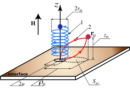
Let us consider the contact described in Sec. II, now placed in a magnetic field directed along the contact axis, Figure 8 shows schematically the trajectories of the electrons that are injected into the metal and interact with the defect.
In what follows the Schrödinger equation is solved along the same lines as in Sec. II, and as zeroth approximation we use the well-known wave function for an electron in a homogeneous magnetic field. In Ref. Avotina07 the dependence of the STM conductance on magnetic field has been obtained under the assumptions that the contact diameter is much smaller than the magnetic quantum length, the radius of the electron trajectory, is much smaller than the mean free path of the electrons, , and the separation between the magnetic quantum levels, the Landau levels, is larger than the temperature , ( is the Larmor frequency). Although these conditions restrict the possibilities for observing the oscillations severely, all conditions can be realized, e.g., in single crystals of semimetals (Bi, Sb and their ordered alloys) where the electron mean free path can be up to millimeters and the Fermi wave length m. Under condition of the inequalities listed the dependence of the conductance of the tunnel point contact on is given by Avotina07
| (62) |
Here
| (63) |
, and are Laguerre polynomials, , is the spin index, is the number of electron states for one spin direction per unit volume at the Fermi energy,
| (64) |
is the maximum value of the quantum number for which and is the integer part of the number , is the conductance in absence of a defect,
| (65) |
The conductance (65) undergoes oscillations having the periodicity of the de Haas-van Alphen effect that originates from the step-wise dependence of the number of electron states (64) on the magnetic field. At (semiclassical approximation), Eq.(65) can be expanded in the small parameter
| (66) |
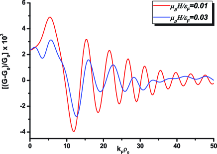
where is the conductance of the contact at (see Eq. (59)).
The oscillatory part of the conductance, which results from the electron scattering on the defect, is plotted in Fig. 9 for a defect placed at . Figure 10 illustrates the dependence of the conductance (62) on coordinate of the defects for different The beating of the oscillation amplitude due to the difference of electron energies for different spin is seen at higher magnetic field.
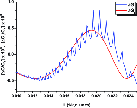
The dependence plotted in Fig. 9, (62), contains oscillations with different periods. The semiclassical asymptotes at of the expression for the conductance Eq. (62) allows us to explain the physical origin of these oscillations. By using the Poisson summation formula in Eq. (62) the part of the conductance related with the scattering by the defect can be written as a sum of two terms
| (67) |
each of them describing conductance oscillations with different periods, which are discussed in more detail below.
VI.2 Effect of flux quantization through the trajectory of the scattered electrons
The first term in Eq. (67) describes the long-period oscillations
| (68) |
where is the flux quantum. The flux, is given by the field lines penetrating the areas of the projections on the plane of the trajectories of the electrons moving from the contact to the defect and back (see, the trajectory 2 in Fig. 8). Such trajectories consist of two arcs, and there are a lot of trajectories with different As was shown in Refs. Avotina07 among these trajectories the signal is dominated by the one that has minimal area given by . Here is the area of the segment formed by the chord of length and the arc of radius , with the angle between the vector and the -axis, Therefore, the oscillation disappears when the defect sits on the contact axis, Obviously, the origin of these oscillations lies in the curvature of the electron trajectories in a magnetic field. As we can see from Eq. (68) the oscillations in the conductance have a nature similar to the Aharonov-Bohm effect (the conductance undergoes oscillations with a period ) and are related to the quantization of the magnetic flux through the area enclosed by the electron trajectory. For illustration of this fact in Fig. 9 the full expression for the oscillatory part of the conductance (the second term in Eq. (62)) is compared with the semiclassical approximation , Eq (68).
For the observation of the Aharonov-Bohm-type oscillations the position of the defect in the plane parallel to the interface must be smaller then , i.e. the defect must be situated inside the ‘tube’ of electron trajectories passing through the contact. At the same time the inequality must hold in order that a magnetic flux quantum is enclosed by the area of the closed trajectory.
VI.3 Effect of longitudinal focusing of electrons on the defect by the magnetic field
The short-period oscillations originate from the effect of the electron being focused by the magnetic field, and is described by the term in Eq. (67). At this term can be written as
| (69) |
In the absence of a magnetic field only those electrons that are scattered off the defect in the direction directly opposite to the incoming electrons can come back to the point-contact. When the electrons move along a spiral trajectory and may come back to the contact after scattering under a finite angle to the initial direction (the trajectory 1 in Fig.8). For example, if the defect is placed on the contact axis an electron moving from the contact with a wave vector along the magnetic field returns to the contact when the -component of the momentum , for integer . For these orbits the time of the motion over a distance in the direction is a multiple of the cyclotron period . Thus, after revolutions the electron returns to the contact axis at the point The phase which the electron acquires along the spiral trajectory is composed of two parts, The first, is the ‘geometric’ phase accumulated by an electron with wave vector over the distance . The second, is the phase acquired during rotations in the field where is the radius of the spiral trajectory. Substituting and in the equation for we find
| (70) |
This is just the phase shift that defines the period of oscillation in the contribution (69) to the conductance. It describes a trajectory which is straight for the part from the contact to the defect and spirals back to the contact by windings as it is shown in Fig.8. There are trajectories consisting of helices in the forward and reverse paths, with and coils, respectively. However, the contribution of these trajectories to the conductance is smaller than (69) by a factor Note that, although the amplitude of the oscillation (69) is smaller by a factor than the amplitude of the contribution (68), the first depends on the depth of the defect as while The slower decreasing of the amplitude for is explained by the effect of focusing of the electrons in the magnetic field. The predicted oscillations, Eq. (69), are not periodic in nor in . Their typical period can be estimated as the difference between two nearest-neighbor maxima
| (71) |
The period (71) depends on the position of the defect. It is larger than the period of de Haas-van Alphen oscillation, Both of these periods are of the same order of magnitude.
VII Nonmagnetic defect in a superconductor
In this section we present the results of a theoretical investigation of the conductance, , of a normal metal - superconductor (NS) point contact (with radius ) in the tunnelling limit and discuss the quantum interference effects originating from the scattering of quasiparticles by a point-like nonmagnetic defect Avotina08ns . The model is described in Sec. II and illustrated in Fig. 1, modified with having the half-space occupied by a (-wave) superconductor. At zero temperature a tunnel current flows through the contact for an applied bias larger than the energy gap of the superconductor . In order to evaluate the total current through the contact, , the current density of quasiparticles with momentum at formed by electrons transmitted through the contact must be found. The current density is expressed in terms of the coefficients and of the canonical Bogoliubov transformation Hard . The functions and satisfy the Bogoliubov-de Gennes (BdG) equations Gennes , which must be supplemented with a self-consistency condition for the order parameter , and boundary conditions which connect and in the normal metal to those in the superconductor at the contact. For a tunnel contact one can neglect Andreev reflections, because these lead to corrections to the conductance proportional to BTK ; the functions and satisfy the same boundary conditions (10), (11) as the wave function for a contact between normal metals.
It is obvious that the method described in Sec. II and Sec. III can be generalized to NS contacts. As a first step the Bogoliubov-de Gennes (BdG) equations must be solved in linear approximation in the transmission amplitude in the absence of the defect, after which the corrections due to the scattering by the defect can be found. In Ref. Avotina08ns an analytical solution for the BdG equations was found with the approximation of a homogeneous order parameter
At small applied bias ( is the Debye frequency), and in linear approximation in the electron-defect interaction constant the conductance of a NS tunnel point contact can be presented as the sum of two terms,
| (72) |
The first term, , in Eq. (72) is the conductance of the NS tunnel point contact in the absence of the defect
| (73) |
where is the conductance of a contact between normal metals (27 ), which is multiplied by the normalized density of states of the superconductor at . Although such result is not unexpected and has been confirmed by experiment Pan , for a contact of radius it was not obvious and it is first obtained in Ref. Avotina08ns . The second term describes the oscillatory dependence of the conductance with the distance between the contact and the defect. If the defect is situated in the superconductor
| (74) |
where
| (75) |
| (76) |
and the function is given by Eq. (29). Equation (74) is obtained by neglecting all small terms of the order of and . Note that we kept the second term in square brackets in the formula for (Eq. (76)) because for large the phase shift of the oscillations may be important.
VIII Conclusions
Thus, we have reviewed some theoretical aspects of the possibility of investigating subsurface defects by STM experiments. The theoretical results show that the amplitude of the oscillations of the STM conductance resulting from quantum interference of electron waves injected by the STM tip and scattered by the defect remains sufficiently large (), even for defects located more than 10 atomic layers below the surface. For example, in the STM experiments of Ref. Stipe signal-to-noise ratios of (at 1 nA, 400 Hz sample frequency) have been achieved. Recently, the possibility of observing defects at such depths below the surface has been demonstrated in experiment Weismann .
The STM tip plays the role of ”locator”, which detects a defect below the metal surface by using electron waves. The defect in turn produces information about its (defect) characteristics, as well as showing properties of the host metal by producing Friedel-like oscillations in the STM conductance. The phase of the oscillations, is defined by the Fermi wave vector and the tip-defect distance One of the possibilities to determine the defect depth below surface is by changing the maximal value of the wave vector by accelerating the electrons with an applied bias Avotina05 ; Avotina09ltp25 . When the tip is situated above the defect, the period of the oscillations in , , uniquely defines As the period of the oscillations becomes longer for small the minimum detectable depth will be determined by the maximum voltage that can be applied over the junction. For example, 30 mV is sufficient for probing a quarter of a conductance oscillation caused by a defect at 1 nm depth.
Another factor in setting the oscillation phase is the shape of the Fermi surface (FS). As was shown, for an anisotropic FS the phase and amplitude of conductance oscillations depend on the characteristics of the FS in the point for which the direction of the velocity is parallel to the vector directed from the STM tip to the defect Avotina06 . Namely, the phase of the oscillations is defined by the projection of on the direction of and the oscillation amplitude depends on the curvature of the FS. Depending on the geometry of the FS there can be several points with the same direction of the velocity, or, if the FS has open parts, certain directions of the velocity can be forbidden. It follows from the results above that curves of constant phase (maxima and minima) in the interference pattern of the STM conductance show the contours formed by projections of the vector on the vector normal to the FS. Although such contours reflect the main features of the FS geometry, they cannot be considered as a direct imaging of the FS.
Electron scattering by subsurface magnetic defects in STM conductance possesses some features distinct from the scattering by magnetic adatoms and the form and sign of the Kondo anomaly due to a subsurface magnetic defect depend on the depth Avotina08mi . Near the Kondo resonance the scattering phase shift tends to , and including multiple electron scattering events after reflections by the metal surface becomes essential. This explains the appearance of harmonics in the oscillatory part of the conductance, which have an additional phase shift where is the number of electron reflections by the surface. The determination of this phase shift near the Kondo resonance and far from it (where ) for the first and second harmonics provides an alternative way to find the depth of the defect
The possibilities of investigating magnetic defects are extended by injecting a spin-polarized current. If the subsurface cluster possesses an unscreened magnetic moment , the scattering amplitudes of spin-up and spin-down electrons are different. This results in a dependence of the oscillation amplitude on the angle between the vector and the polarization direction of the STM current - referred to as a magneto-orientational effect Avotina09 .
A strong magnetic field perpendicular to the metal surface changes the interference pattern in the STM conductance fundamentally. As a result of Zeeman splitting of the Landau energy levels the interference patterns formed in the dependence by electrons with different spin directions do not coincide because of different electron wave lengths for energies The superposition of the two oscillatory parts may result in a beating of the total amplitude of the oscillations. Along with the well-known quantum oscillations having the periodicity in of the de Haas - van Alphen effect in the STM conductance, in the presence of a defect two new types of oscillations are present. The first is related to flux quantization through the projection of the electron trajectory on the surface plane. The second type of oscillation is related to a focusing effect of the magnetic field. As in Sharvin’s two-point contact experiments, in which electrons were focused on a collector by a magnetic field directed along the line connecting the contacts (geometry of longitudinal electron focusing) Sharvin , the magnetic field can periodically focus the electrons injected by the tip onto the defect. This results in periodic increasing or decreasing of the part of the conductance related to the scattering by the defect Avotina07 .
If the electrons tunnel from a normal-metal STM tip into a superconductor the wave incident on the contact is transformed into a superposition of ‘electron-like’ and ‘hole-like’ quasiparticles. In the case of a location of the defect in the superconductor quantum interference takes place between the partial wave that is transmitted and the one that is scattered by the defect, for both types of quasiparticles independently (Eq. (74)). Although the difference between wave vectors of ‘electrons’ and ‘holes’ is small the shift between the two oscillations should be observable Avotina08ns .
References
- (1) G. Binnig, H. Rohrer, IBM Journal of Research and Development 30, 4 (1986).
- (2) J. Friedel, Nuovo Cimento, 7, 287 (1958).
- (3) J. M. Ziman, Principles of the theory of solids, Cambrige Univ. Press (1964).
- (4) M. F. Crommie, C. P. Lutz, and D. M. Eigler, Nature 363, 524 (1993); ibid., Science 262, 218 (1993).
- (5) Y. Hasegawa, P. Avouris: Phys. Rev. Lett. 71, 1071 (1993).
- (6) L. Bürgi, N.Knor, H. Brune, M.A. Schneider, K. Kern, Appl. Phys. A 75, 141 (2002).
- (7) L. Petersen, B. Schaefer, E. Lagsgaard, I. Stensgaard, F. Besenbacher, Surface Science 457, 319–325 (2000).
- (8) P.T. Sprunger, L. Petersen , E.W. Plummer, E. Lagsgaard and F. Besenbacher, Science 275, 1764 (1997).
- (9) F. Vonau, D. Aubel, G. Gewinner, C. Pirri, J. C. Peruchetti, D. Bolmont, and L. Simon, Phys. Rev. B 69, 081305 (2004).
- (10) V. Madhavan , W. Chen, T. Jamneala, M.F. Crommie and N.S. Wingreen, Science 280, 567 (1998).
- (11) J. Li, W.-D. Schneider, R.Berndt and B. Delley, Phys. Rev. Lett. 80, 2893 (1998),
- (12) W. Chen, T. Jamneala, V. Madhavan and M. F. Crommie, Phys. Rev. B, 60, R8529 (1999).
- (13) N. Knorr, M.A.Schneider, L. Diekhöner, P. Wahl and K. Kern, Phys. Rev. Lett. 88, 096804 (2002).
- (14) U. Fano, Phys. Rev., 124, 1866 (1961).
- (15) M. Plihal and J.W. Gadzuk, Phys. Rev. B, 63, 085404 (2001).
- (16) P. Wahl, L. Diekhöner, M. A. Schneider, L. Vitali, G. Wittich, and K. Kern, Phys. Rev. Lett. 93, 176603 (2004).
- (17) H.P. Manoharan, C.P. Lutz and D.M. Eigler, Nature 403, 512 (2000).
- (18) G.A. Fiete, E.J. Heller, Rev. Mod. Phys. 75, 933 (2003).
- (19) O.Yu. Kolesnychenko, R. de Kort, M.I. Katsnelson, A.I. Lichtenstein and H. van Kempen, Nature, 415, 507 (2002).
- (20) S. H. Pan, E. W. Hudson, K. M. Lang, H. Eisaki, S. Uchida, and J. C. Davis, Nature 403, 746 (2000).
- (21) Ali Yazdani, B. A. Jones, C. P. Lutz, M. F. Crommie, D. M. Eigler, Science 275, 1767 (1997).
- (22) S. H. Pan, E. W. Hudson, and J. C. Davis, Appl. Phys. Lett. 73, 2992 (1998).
- (23) M. Xu, Z. Xiao, M. Kitahara, and D. Fujita, Jap. J. Appl. Phys. 43, 4687 (2004).
- (24) M. Bode, Rep. Prog. Phys., 66, 523 (2003).
- (25) H.C. Manoharan, Nature 416, 24 (2002).
- (26) C. Durkan, and M.E. Welland, Appl. Phys. Lett. 80, 458 (2002).
- (27) O. O. Brovko, V. S. Stepanyuk, Phys. Status Solidi B 1–9 (2010)
- (28) S. Crampin, J. Phys.: Condens. Matter 6, L613 (1994).
- (29) M. Schmid, W. Hebenstreit, P. Varga and S. Crampin, Phys. Rev. Lett. 76, 2298 (1996).
- (30) O. Kurnosikov, O.A.O. Adam, H.J.M. Swagten, W.J.M. de Jonge, B. Koopmans, Phys. Rev. B 77, 125429 (2008).
- (31) Hongbin Yu, C. S. Jiang, Ph. Ebert, and C. K. Shih, Appl. Phys. Lett. 81, 2005 (2002).
- (32) N. Quaas, M. Wenderoth, A Weismann, R. G. Ulbrich and K. Schönhammer, Phys. Rev. B 69 201103(R) (2004).
- (33) A. Weismann, M. Wenderoth, S. Lounis, P. Zahn, N. Quaas, R. G. Ulbrich, P. H. Dederichs, S. Blügel, Science 323, 1190 (2009).
- (34) W. A. Hofer, A. Foster, and A. Shluger, Rev. Mod. Phys. 75, 1287 (2003).
- (35) J. M. Blanco, F. Flores, R. Pèrez, Progress in Surface Science, 81, 403 (2006).
- (36) I. O. Kulik, Yu. N. Mitsai, and A. N. Omelyanchouk, Zh. Exp. Teor. Fiz. 63, 1051 (1974).
- (37) V. Bezàk, J. of Math. Phys. 48, 112108 (2007).
- (38) V. Bezàk, Applied Surface Science 254 3630, (2008).
- (39) A. V. Balatsky, I. Vekhter, and Jian-Xin Zhu, Rev. Mod. Phys. 78, 373 (2006).
- (40) V. S. Stepanyuk, A. N. Baranov, D. V. Tsivlin, W. Hergert, P. Bruno, N. Knorr, M. A. Schneider, and K. Kern, Phys. Rev. B 68, 205410 (2003).
- (41) E. L. Wolf, Principles of Electron Tunneling Spectroscopy, Oxford University Press, New York and Claredon Press, Oxford, 1985.
- (42) K. Kobayashi, Phys. Rev. B 54 17029 (1996).
- (43) J. Tersoff, D. Hamann, Phys. Rev. B 31 805 (1985).
- (44) I.M. Lifshits, M.Ya. Azbel’, and M.I. Kaganov, ”Electron theory of metals”, New York, Colsultants Bureau (1973).
- (45) E. Granot and M.Ya. Azbel, Phys. Rev. B 50, 8868 (1994); J. Phys. Condens. Matter 11, 4031 (1999).
- (46) Ye. S. Avotina, Yu. A. Kolesnichenko, and J.M. Ruitenbeek, J. Phys.: Condens. Matter 20, 115208 (2008).
- (47) Ye. S. Avotina, Yu. A. Kolesnichenko, and J.M. Ruitenbeek, Low Temp. Phys., 34, 936 (2008).
- (48) C. Untiedt, G. Rubio Bollinger, S. Vieira, and N. Agraït, Phys. Rev. B 62, 9962 (2000).
- (49) B. Ludoph, M. H. Devoret, D. Esteve, C. Urbina, and J. M. van Ruitenbeek, Phys. Rev. Lett. 82, 1530 (1999).
- (50) A.M. Kosevich, Fiz. Nizk. Temp., 11, 1106 (1985) [Sov. J. Low Temp. Phys., 11, 611 (1985)] .
- (51) Ye. S. Avotina, Yu. A. Kolesnichenko, A.N. Omelyanchouk, A.F. Otte, and J.M. Ruitenbeek, Phys. Rev. B 71, 115430 (2005).
- (52) Yu.A. Aminov, ”Differential geometry and topology of curves”, Moskow, ”Nauka” (1987) (in Russian).
- (53) A.A. Abrikosov, Fundamentals of the theory of metals, North Holland, 1988.
- (54) M.A. Schneider, L. Vitali, N. Knorr and K. Kern, Phys. Rev. B, 65, 121406 (2002).
- (55) Ye. S. Avotina, Yu. A. Kolesnichenko, A.F. Otte, and J.M. Ruitenbeek, Phys. Rev. B, 74, 085411 (2006).
- (56) Arthur P. Cracknell, The Fermi surfaces of metals: a description of the Fermi surfaces of the metallic elements, Taylor and Francis, London (1971).
- (57) O. Újsághy, J. Kroha, L. Szunyogh and A. Zawadowski, Phys. Rev. Lett., 85, 2557 (2000).
- (58) Chiung-Yuan Lin, A.H. Castro Neto and B.A. Jones, Phys. Rev. B, 71, 035417 (2005).
- (59) P.W. Anderson, Phys. Rev., 124, 41 (1961).
- (60) A. Kubetzka, M. Bode, O. Pietzsch, and R. Wiesendanger, Phys. Rev. Lett. 88, 057201 (2002).
- (61) J. Frenkel and J. Dorfman, Nature 126, 274 (1930).
- (62) S.V. Vonsovsky, Magnetism, John Wiley & Sons, New York (1974).
- (63) J. C. Slonczewski, Phys. Rev. B 39, 6995 (1989).
- (64) M. Morgenstern, R. Dombrowski, Chr. Wittneven, and R. Wiesendanger, Phys. Stat. Sol. (b) 210, 845 (1998).
- (65) A. Cano and I. Paul, Phys. Rev. B 80, 153401 (2009).
- (66) Ye. S. Avotina, Yu. A. Kolesnichenko, A.F. Otte, and J.M. Ruitenbeek, Phys. Rev. B 75, 125411 (2007).
- (67) Ye. S. Avotina, Yu. A. Kolesnichenko, and J.M. Ruitenbeek, Phys. Rev. B 80, 115333 (2009).
- (68) Ye. S. Avotina, Yu. A. Kolesnichenko, S.B. Roobol and J.M. Ruitenbeek, Low Temp. Phys., 34, 207 (2008).
- (69) F.J. Jedema, H.B. Heersche, A.T. Fllip, L.L.A. Baselmans, and B.J. van Weels, Nature 416, 713 (2002).
- (70) M. Hard, S. Datta, and P.F. Bagwell, Phys. Rev. B 54, 6557 (1996).
- (71) P. G. de Gennes, Superconductivity of Metals and Alloys (W.A. Benjamin, Inc. New York, 1966).
- (72) G.E. Blonder, M. Tinkham, T.M. Klapwijk, Phys. Rev. B 25, 4515 (1982).
- (73) B. C. Stipe, M. A. Rezaei, and W. Ho, Rev. Sci. Instr. 70, 137 (1999).
- (74) Ye. S. Avotina, Yu. A. Kolesnichenko, and J.M. Ruitenbeek, J. Phys.: Conf. Series 150 022045 (2009).
- (75) Yu.V. Sharvin, JETP Lett., 1, 152 (1965).