Fast readout of a single Cooper-pair box using its quantum capacitance
Abstract
We have fabricated a single Cooper-pair box (SCB) together with an on-chip lumped element resonator. By utilizing the quantum capacitance of the SCB, its state can be read out by detecting the phase of a radio-frequency (rf) signal reflected off the resonator. The resonator was optimized for fast readout. By studying quasiparticle tunneling events in the SCB, we have characterized the performance of the readout and found that we can perform a single shot parity measurement in approximately 50 ns. This is an order of magnitude faster than previously reported measurements.
pacs:
85.25.Cp, 73.23.Hk, 42.50.DvI Introduction
Superconducting devices based on Josephson junctions have successfully been used in many different kinds of applications, including very sensitive magnetometers based on superconducting interference devices (SQUIDs), bolometric detectors, mixers, and parametric amplifiers. They have also been suggested to be strong candidates as building blocks for a quantum computer Makhlin et al. (2001); Plantenberg et al. (2007); McDermott et al. (2005); Koch et al. (2007). They are easily fabricated with standard lithographic techniques and can be integrated with other electrical circuits. This gives them the potential to be scalable. Devices utilizing charging effects include very small tunnel junctions. Such Coulomb blockade devices, are also widely used in measurements, for example, the single electron transistors (SET)Fulton and Dolan (1987). The radio frequency version of the SET is the worlds most sensitive electrometer Schoelkopf et al. (1998); Brenning et al. (2006).
The single Cooper-pair box (SCB) Büttiker (1987); Bouchiat et al. (1998); Nakamura et al. (1999) is one of the simplest Coulomb blockade devices, involving a single Josephson junction. SCBs are very sensitive to the presence of quasiparticles which suggested its use as potential radiation detector Shaw et al. (2009a). The presence of quasiparticles can be measured by detecting the charge on the SCB island using an external SET Ferguson et al. (2006). In this paper, we characterize an intrinsic method for reading out the SCB which relies on the curvature of its energy bands. This methods is both faster and is predicted to have less backaction then using a SET. The curvature of the energy bands of the SCB (with respect to gate charge) gives rise to the so called quantum capacitance Duty et al. (2005); Sillanpää et al. (2005) and has been utilized in a number of experiments, for example in the measurements on longitudinal dresses states of a driven SCB Wilson et al. (2007, 2010). It has also been used to study the ground state of two coupled qubits Shaw et al. (2009b), and to study quasiparticle poisoning of a SCB qubit Shaw et al. (2008). In Ref. Shaw et al., 2008 they used a resonator with a bandwidth of 200 kHz which limited the speed the their measurements. Here we use the random tunneling of quasiparticles to characterize the performance of the quantum capacitance readout. We show that we can measure the state of the SCB an order of magnitude faster than has previously been reported, including measurements using RF-SETs. We also show that we can prepare the SCB in a certain parity state with a high probability.
II Theory
II.1 Cooper-pair box
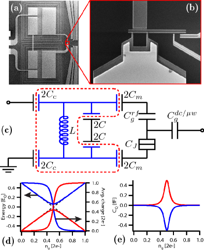
The sample under investigation is a SCB and is shown in Fig. 1(a) & (b). The SCB consist of a superconducting island connected to a large reservoir by a Josephson junction. The Josephson junction is made in a SQUID-configuration to allow the Josephson energy, , to be tuned by applying a magnetic field through the loop. The SCB is also characterized by the electrostatic energy, , which is the energy required to add an extra Cooper pair to the island. Here is the number of Cooper pairs that have tunneled onto the island and is the normalized gate voltage, where is the capacitance between the voltage source and the island. If the capacitance of the island, , is small enough the Cooper-pair charging energy, , will dominate over the Josephson energy, , and the temperature, . In this case the charge fluctuation on the island will be small. The number of excess Cooper pairs on the island, , is then a good quantum number and the charge of the island can be well controlled by the external gate voltage, . For and , only two charge states will be of interest: and , corresponding to zero () or one () extra Cooper pair on the island. Then the Hamiltonian of the Cooper-pair box can be written
| (1) |
where , are the Pauli spin matrices. Here we have ignored all state independent terms of the Hamiltonian. The two eigenenergies for this Hamiltonian are plotted in Fig. 1(d) as a function of . At the degeneracy point , where the electrostatic energies of the two charge states cross, we get an avoided level crossing with a splitting between the ground and excited state equal to . In the same graph, we have also plotted the expectation value of the island charge for each energy eigenstate.
II.2 Quantum Capacitance
At the degeneracy point the energy difference between the ground and excited state is, to first order, independent of the gate charge , which makes this the ideal bias point when the SCB is used as a qubit. At this point, the longest dephasing times are obtained Vion et al. (2002). Therefore, this is often called the optimal point. If we want to detect the state of the SCB sitting at the optimal point, we cannot measure the charge, since the charges of the ground and exited state are the same at this point (see Fig. 1(d)). Although the charges are the same for the two states, the derivatives of the charges with respect to the gate voltage differ and can be used for readout. We can define an effective capacitance of the SCB by calculating , where is the average value of the injected charge on the gate capacitor. This effective capacitance, , will have two contributions, a geometric part consisting of the gate capacitance in series with the junction capacitance, and a state dependent part that we call the quantum capacitance Duty et al. (2005). This quantum capacitance, , takes the following form
| (2) |
for the ground (g) and first excited (e) state, where and is the energy difference between the two states at a given . is equal in magnitude but has opposite signs for the ground and excited state, with being negative for the ground state. In Fig. 1(e), is plotted against the gate charge, , for the ground and exited state of the SCB.
If we embed the SCB in a resonant tank circuit (see Fig. 1(c)) the effect of the quantum capacitance will be to shift the resonance frequency. The reflection coefficient, , of the resonator has a constant magnitude, i.e. , since there are no dissipative element in the resonator. The phase , however has a sharp frequency dependence and close to the resonance frequency of the tank circuit, , the phase, , can be approximated by the expression:
| (3) |
where is the angular probe frequency and is the external quality factor of the resonator. Now, if the capacitance of the SCB is changed by a magnitude of , the phase of the rf signal at frequency reflected off the resonator will change by:
| (4) |
Here we have treated the resonator purely classically. A full quantum treatment, including the SCB, resonator and transmission line can be found in the work of Johansson et al. Johansson et al. (2006). It is shown that this method of readout is quantum limited Johansson et al. (2006), meaning that no information is lost during the readout (no extra dephasing).
II.3 Quasiparticles
Quasiparticles are single-particle excitations of the superconducting condensate. Quasiparticle fluctuations have been studied as a source of noise in superconducting devices for some time. Thermodynamic fluctuations in the quasiparticle number, also know as generation-recombination noise, is an important source of noise at intermediate temperatures Wilson et al. (2001a). Time-resolved measurements of these fluctuations have shown very good agreement between theory and experiment Wilson and Prober (2004); Wilson et al. (2001b). At very low temperatures, were thermal quasiparticles should be suppressed, a significant population of quasiparticles is still observed in most experiments. The origin of these nonequilibrium quasiparticles is still unknown. However, it is clear that they remain an important source of noise.
The most significant source of quasiparticle noise in a SCB is commonly referred to as quasiparticle poisoning. When a nonequilibrium quasiparticle in the reservoir tunnels onto the SCB island, it shifts the potential of the island by . The random tunneling of quasiparticles on and off of the island, therefore leads to a large-amplitude telegraph noise in the island potential. Quasiparticle poisoning has been extensively studied Shaw et al. (2008); Aumentado et al. (2004); Lutchyn and Glazman (2007), including the observation of individual tunneling events in real time Ferguson et al. (2006); Naaman and Aumentado (2006). It has been shown that poisoning is well described by a simple kinetic model, starting from the assumption of a finite density of nonequilibrium quasiparticles in the leads. In this model, the tunneling rates are then dictated by the relative energies of the even (no quasiparticles on the island) and odd (one quasiparticle on the island) states. If the energy of the odd state is lower than the even state, the quasiparticle can be trapped on the island (see Fig. 3(a)). The energy difference of the even and odd state is maximum at the charge degeneracy point, , where it takes the value . Here and are the superconducting energy gap of the island and the reservoir, respectively. The average occupation of the two states is then simply determined by the Boltzmann factor .
III Device design and fabrication
When designing the readout circuit there is a trade off between having a good signal (large phase shift) and a low backaction. The phase shift is roughly proportional to (see equation 4), meaning that for a fixed Q-value (i.e. measurement bandwidth) we want a small total capacitance in the resonator (and a large inductance). However, the voltage noise of the environment will induce charge fluctuations on the SCB, with a magnitude that scales with the same prefactor. Thus, by decreasing the total capacitance in the resonator, , you can increase the sensitivity (larger phase shift) at the cost of a larger backaction on the SCB.
The Q-value of the resonator sets the bandwidth, i.e. an upper limit on how fast we can measure. We designed the resonator to have an external Q-value of 100 which corresponds to a time constant of 50 ns at MHz. The internal Q-value is usually substantially larger and can therefore be ignored.
The devices were fabricated in a multilayer process. Starting from a high-resistivity silicon wafer with a native oxide, the wafer was first cleaned using rf back sputtering directly after which a 60 nm thick layer of niobium was sputtered. To pattern the niobium, we used a 20 nm thick Al mask made by e-beam lithography and e-beam evaporation. The niobium was then etched in a CF4 plasma (with a small flow of oxygen) to form the inductor and bottom plates of the capacitors (see Fig. 1(c)). The choice of niobium for the bottom layer made it possible to test the resonator in liquid helium (even with a top layer made of normal metal, e.g. gold). The Al mask was removed with a wet-etch solution based on phosphoric acid. Before depositing the insulator we cleaned the wafer in a 2% HF solution for 30 sec in order to remove most of the niobium oxide which has been found to degrade the Q-value of the niobium resonators. Using PE-CVD, we then deposited an insulating layer of 200 nm of silicon nitride. The silicon nitride layer covers the whole wafer; connections to the niobium layer are only made through capacitors. We chose silicon nitride since it is known to have low dielectric losses Martinis et al. (2005). After using a combination of DUV photolithography to define bonding pads along with e-beam lithography to define quasiparticle traps Rooks et al. (1987), a 3/80/10 nm thick layer of Ti/Au/Pd was deposited by e-beam evaporation. Finally, the layer containing the SCB was made by e-beam lithography and two-angle shadow evaporation of 10+30 nm of aluminum, with 6 min of oxidation at 4 mbar. The thickness of the island (10 nm) was chosen to be much thinner than for the reservoir (30 nm) in order to enhance the superconducting gap, , of the island compared to the reservoir. This was done to reduce quasiparticle poisoning.
IV Measurements
IV.1 Measurement setup
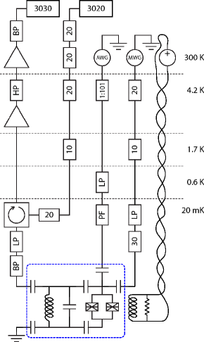
The device was cooled in a dilution refrigerator with a base temperature of about 20 mK. For the readout, we used an Aeroflex 3020 signal generator to produce the rf signal. The signal was heavily attenuated and filtered and was fed to the tank circuit via a Pamtech circulator positioned at the mixing chamber. The reflected signal was amplified by a Quinstar amplifier at 4K with a nominal noise temperature of 1 K. The in-phase and quadrature components of the signal were finally measured using an Aeroflex 3030 vector digitizer. A schematic of the measurement setup can be found in Fig. 2.
IV.2 Device characterization
In the following sections we will show measurements of two different devices, referred to as sample A and sample B. In order to characterize the devices and extract parameters, the resonator was first measured using a network analyzer. From the measured phase response we could extract the resonance frequency, , and the Q-value of the resonator. We could extract both the Cooper-pair charging energy, , and the maximum Josephson energy, by conventional spectroscopy, while applying a perpendicular magnetic field through the SQUID loop of the SCB, and thereby tuning . Finally by measuring as a function of gate charge, we can extract the rf gate capacitance and the total resonator capacitance. From the expression for the Q-value and the resonance frequency, we can then extract the parameters for the individual components of the resonator. The extracted parameters for the two devices are presented in Table 1. The values of the parameters for sample B corresponds reasonable well to the geometrically identical device that was used in Ref. Persson et al., 2010. The gate capacitance for sample A roughly agrees with what you would expect from the 5 m island compared the to the capacitance of the 8 m island in sample B. If we the insert the parameters from Table 1 into Eq. (4) we calculate an expected phase shift of 11 deg for sample A and 30 deg for sample B between the two parity states when biased at the degeneracy point.
| Sample A | Sample B | |
|---|---|---|
| 676 MHz | 663 MHz | |
| 128 | 130 | |
| 151 nH | 324 nH | |
| 251 fF | 97 fF | |
| 116 fF | 81 fF | |
| 0.2 fF | 0.3 fF | |
| 62 GHz | 48 GHz | |
| 7.2 GHz | 7.4 GHz |
IV.3 Readout performance
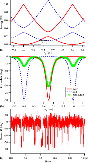
We have fabricated and measured a number of samples. All devices we have measured so far have been poisoned, meaning that quasiparticles cause switching between the two parity states of having an even or odd number of quasiparticles on the island. The switching between these parities happens on the time scale of a few microseconds. Although this is far from ideal for many applications, it has given us a way to characterize the readout. When a quasiparticle tunnels on or off the island the quantum capacitance of the SCB will change, and can thus be detected as a change in the reflected phase from the resonator. The measured time averaged phase for sample B is shown in Fig. 3(b) as function of . In Fig. 3(c) we show the time dependence of the phase measured at the degeneracy point, . Most of the time the SCB is in the odd state with a phase shift of about 0 degrees, however now and then the extra quasiparticle escapes the island and the SCB spends short periods in the even state with a phase shift close to -30 degrees.
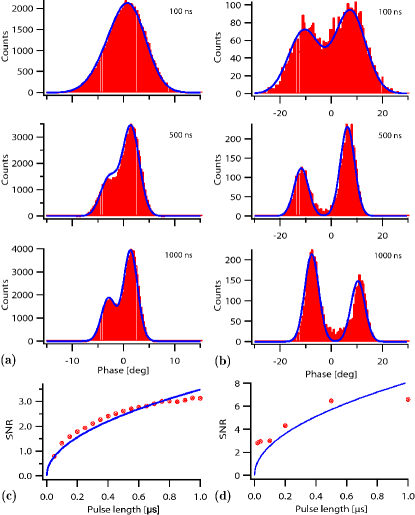
While sitting at the degeneracy point, , we have also performed pulsed measurements of the state. We send down a Gaussian pulse, with a length defined as the full width at half maximum (FWHM), and measure the phase of the reflected pulse. In order to optimize the signal to noise of the measured response, we used a so-called matched filter, where the time traces of the measured in-phase and quadrature component (I and Q) are multiplied with a Gaussian template (with the same shape as the one generated by the signal generator). The product is then integrated and a single value for is extracted. This is done for both I and Q and we can calculate the phase by . We perform 100 000 of these measurements and make histograms of the measured phase and see two peaks centered at different phases corresponding to the two parity states. We fit a double Gaussian (both with the same standard deviation) to the histograms (see Fig. 4(a,b)). We define the signal-to-noise ratio (SNR) of the measurement as the peak separation divided by the standard deviation. This is performed for different pulse lengths and we extract the SNR as a function of the measurement time, Fig. 4(c,d). The SNR roughly follows the expected square root dependence on the measurement time. To reach a SNR we need a pulse length of the order of 50-100 ns in both samples. The shortest measurement time was here limited by the time constant of resonator which was about 60 ns for both of the samples.
IV.4 Quasiparticle relaxation and state preparation
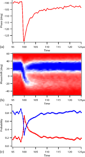
We know that by sitting at the even degeneracy point the system will eventually relax into the odd parity state given that (see Fig. 3). We wanted to study how fast this process is and to what extent you can prepare the SCB in a certain parity state. We start by letting the system equilibrate biased at the odd degeneracy point, i.e. , thereby preparing the even state. We then pulse the gate to the even degeneracy point (at s) and observe the dynamics. From a long time trace, including 1000 pulses, we divide each repetition into 0.5 s increments. We extract the average phase from each increment and each repetition. We then make a histogram of the phase for each increment as a function of time (see Fig. 5(b)). We fit the histograms to a double Gaussian and extract the occupation probability of the even and odd state as a function of time (see Fig. 5(c)). Sitting a the odd degeneracy point, , there is an equilibrium probability of more than of being in the even state and when we pulse to the even state most of the probability is preserved. Eventually the system equilibrated and then the probability is reduced to . From the relaxation of the probabilities we extract an equilibration time of 2.8 s. As a comparison, we show the average time trace (see Fig. 5(a)) where we have taken the average of the full time traces from different pulses. From this we extract a relaxation rate of 3 s in good agreement. Since the quasiparticle relaxation rate is much longer than the operation and readout times this suggests that, even if the device is poisoned, we should with high probability be able to prepare the box in the even state and perform useful measurements.
V Conclusions
We have fabricated and tested two samples with a SCB together with an on-chip lumped element resonator. The resonators were optimized for readout speed, with a Q-value around 100. We have characterized the readout by employing the effect of quasiparticle poisoning and found that for readout pulses of length 50-100 ns we get a SNR greater then 1.
Acknowledgements.
We thank the members of the Quantum Device Physics and Applied Quantum Physics groups for useful discussions. The samples were made at the nanofabrication laboratory at Chalmers. The work was supported by the Swedish VR and SSF, the Wallenberg foundation, the EU under the project EuroSQIP and by IARPA through ARO award W911NF-09-1-0376.References
- Koch et al. (2007) J. Koch, T. M. Yu, J. Gambetta, A. A. Houck, D. I. Schuster, J. Majer, A. Blais, M. H. Devoret, S. M. Girvin, and R. J. Schoelkopf, Phys. Rev. A 76, 042319 (2007).
- Makhlin et al. (2001) Y. Makhlin, G. Schön, and A. Shnirman, Rev. Mod. Phys. 73, 357 (2001).
- Plantenberg et al. (2007) J. H. Plantenberg, P. C. de Groot, C. J. P. M. Harmans, and J. E. Mooij, Nature 447, 836 (2007).
- McDermott et al. (2005) R. McDermott, R. W. Simmonds, M. Steffen, K. B. Cooper, K. Cicak, K. D. Osborn, S. Oh, D. P. Pappas, and J. M. Martinis, Science 307, 1299 (2005).
- Fulton and Dolan (1987) T. A. Fulton and G. J. Dolan, Physical Review Letters 59, 109 (1987).
- Schoelkopf et al. (1998) R. J. Schoelkopf, P. Wahlgren, A. A. Kozhevnikov, P. Delsing, and D. E. Prober, Science 280, 1238 (1998).
- Brenning et al. (2006) H. Brenning, S. Kafanov, T. Duty, S. Kubatkin, and P. Delsing, J. Appl. Phys. 100, 114321 (2006).
- Nakamura et al. (1999) Y. Nakamura, Y. A. Pashkin, and J. S. Tsai, Nature 398, 786 (1999).
- Bouchiat et al. (1998) V. Bouchiat, D. Vion, P. Joyez, D. Esteve, and M. H. Devoret, Phys. Scr. T76, 165 (1998).
- Büttiker (1987) M. Büttiker, Phys. Rev. B 36, 3548 (1987).
- Shaw et al. (2009a) M. D. Shaw, J. Bueno, P. Day, C. M. Bradford, and P. M. Echternach, Physical Review B (Condensed Matter and Materials Physics) 79, 144511 (2009a).
- Ferguson et al. (2006) A. J. Ferguson, N. A. Court, F. E. Hudson, and R. G. Clark, Phys. Rev. Lett. 97, 106603 (2006).
- Duty et al. (2005) T. Duty, G. Johansson, K. Bladh, D. Gunnarsson, C. Wilson, and P. Delsing, Phys. Rev. Lett. 95, 206807 (2005).
- Sillanpää et al. (2005) M. A. Sillanpää, T. Lehtinen, A. Paila, Y. Makhlin, L. Roschier, and P. J. Hakonen, Phys. Rev. Lett. 95, 206806 (2005).
- Wilson et al. (2007) C. M. Wilson, T. Duty, F. Persson, M. Sandberg, G. Johansson, and P. Delsing, Phys. Rev. Lett. 98, 257003 (2007).
- Wilson et al. (2010) C. M. Wilson, G. Johansson, T. Duty, F. Persson, M. Sandberg, and P. Delsing, Phys. Rev. B 81, 024520 (2010).
- Shaw et al. (2009b) M. D. Shaw, J. F. Schneiderman, J. Bueno, B. S. Palmer, P. Delsing, and P. M. Echternach, Phys. Rev. B 79, 014516 (2009b).
- Shaw et al. (2008) M. D. Shaw, R. M. Lutchyn, P. Delsing, and P. M. Echternach, Phys. Rev. B 78, 024503 (2008).
- Vion et al. (2002) D. Vion, A. Aassime, A. Cottet, P. Joyez, H. Pothier, C. Urbina, D. Esteve, and M. H. Devoret, Science 296, 886 (2002).
- Johansson et al. (2006) G. Johansson, L. Tornberg, and C. M. Wilson, Phys. Rev. B 74, 100504(R) (2006).
- Wilson et al. (2001a) C. M. Wilson, L. Frunzio, K. Segall, L. Li, D. E. Prober, D. Schiminovich, B. Mazin, C. Martin, and R. Vasquez, IEEE Trans. Appl. Supercond. 11, 645 (2001a).
- Wilson and Prober (2004) C. M. Wilson and D. E. Prober, Phys. Rev. B 69, 094524 (2004).
- Wilson et al. (2001b) C. M. Wilson, L. Frunzio, and D. E. Prober, Phys. Rev. Lett. 87, 067004 (2001b).
- Aumentado et al. (2004) J. Aumentado, M. W. Keller, J. M. Martinis, and M. H. Devoret, Phys. Rev. Lett. 92, 066802 (2004).
- Lutchyn and Glazman (2007) R. M. Lutchyn and L. I. Glazman, Phys. Rev. B) 75, 184520 (2007).
- Naaman and Aumentado (2006) O. Naaman and J. Aumentado, Phys. Rev. B 73, 172504 (2006).
- Martinis et al. (2005) J. M. Martinis, K. B. Cooper, R. McDermott, M. Steffen, M. Ansmann, K. D. Osborn, K. Cicak, S. Oh, D. P. Pappas, R. W. Simmonds, et al., Phys. Rev. Lett. 95, 210503 (2005).
- Rooks et al. (1987) M. J. Rooks, S. Wind, P. McEuen, and D. E. Prober, J. Vac. Sci. Technol. B 5, 318 (1987).
- Persson et al. (2010) F. Persson, C. M. Wilson, M. Sandberg, G. Johansson, and P. Delsing, Nano Letters 10, 953 (2010).