Dirac electronic states in graphene systems:
Optical spectroscopy studies
Abstract
Electronic properties of two-dimensional allotropes of carbon, such as graphene and its bilayer, multi-layer epitaxial graphene, few-layer Bernal-stacked graphene, as well as of three-dimensional bulk graphite are reviewed from the viewpoint of recent optical spectroscopy studies. Attention is focused on relativistic-like character of quasi particles in these systems, which are referred to as massless or massive Dirac fermions.
pacs:
81.05.Uw,82.45.Mp,73.20.-r,78.20.-e1 Introduction
The family of carbon-based materials, including two distinct crystal forms: the isotropic diamond and anisotropic graphite, together with other allotropes such as fullerenes and carbon nanotubes, has been recently enlarged to include graphene, a unique material which consists of a two-dimensional (2D) lattice of carbon atoms with a honeycomb symmetry. Graphene, the closest archetype of a two- dimensional crystal, while being very promising for future applications, represents also an extremely interesting system from the viewpoint of fundamental physics [1, 2]. Distinctly, the electronic states of graphene do not obey the conventional laws of Schrödinger’s quantum mechanics but are rather governed by an equation which is equivalent to the Dirac equation for massless fermions [3, 4]. This very peculiar, but at the same time simple, electronic band structure of graphene has been investigated theoretically for more then sixty years [5]. The “rise” of graphene dates however only from 2004 when it was effectively introduced into the the laboratory environment, following the clear identification of 10 m sized graphene flakes deposited on Si/SiO2 substrates [6] and of multi-layer epitaxial graphene thermally decomposed from silicon carbide [7, 8]. More recently, the growth of large area graphene samples on metallic surfaces (Ru, Ni or Cu) [9, 10, 11, 12, 13, 14], and their subsequent transfer on arbitrary substrates has also substantially progressed [12, 14], what may be a promising option for easy preparation of macroscopic-size crystallites of graphene.
The intense, over last years, investigations of different graphene systems have expanded today into a broad research field of qualitatively new two-dimensional systems [15]. The challenging expectation are that graphene will introduce quantum electrodynamics into solid state laboratories [16, 17, 18, 19] and that it will constitute the basis for future electronics plausible avoiding the known limitations (at the nano-scale) of the CMOS technology. As for today, the basic properties of “new” 2D allotropes of carbon, including graphene [3, 4], graphene bilayer [20, 21], multi-layer graphene [6, 22], graphene on a silicon carbide substrate [7], are already relatively well-known and the basis of the graphene physics is pretty well established.
Despite relevant advances in various experimental techniques, such as angular resolved photoemission spectroscopy (ARPES) [23, 24, 25, 26] or scanning tunnelling spectroscopy (STS) [27, 28, 29], a large part of our knowledge on electronic properties of graphene has been deduced from conventional, electric transport and optical experiments, in particular under an applied magnetic field. The physics of the integer quantum Hall effects in single-layer and bilayer graphene [3, 4, 20] or of the minimum conductivity of graphene [30, 31] is nowadays underpinned by a solid basis of published transport experiments. Optical investigations of graphene systems are equally fertile. They offer a rather direct verification of electronic band structure in these materials and/or help to avoid the advanced sample processing of often invasive character [32].
A number of papers which review the graphene-related physics has already appeared within last few years [33, 1, 34, 2, 35, 36, 15], but the progress in this research area is extremely fast. This, in particular, concerns the developments related to optical spectroscopy which was perhaps not very popular at the birth of the research on graphene but it is now more and more frequently used, as testified by a large number of recent papers cited here. As any review article also this one includes some unavoidable repetitions of information which can be found elsewhere. However, our intention is to discuss the properties of different graphene systems from the viewpoint of optical spectroscopy methods, including the most recent developments in this field. Whereas the previous review articles were mostly focused on the properties of a single graphene monolayer, here we discuss the Dirac-like electronic states (massless and massive) which in fact are representative of any two-dimensional allotropes of carbon or even of bulk graphite.
Indeed, the methods of optical spectroscopy have been recently applied to a large class of graphene-based systems. A number of various optical and magneto-optical measurements have been performed on mono-, bi- and multi-layer Bernal-stacked graphene (exfoliated from graphite and placed on Si/SiO2), on multilayer epitaxial graphene thermally decomposed from C-terminated surface of SiC, as well as on bulk graphite. The published papers provide a mosaic of information as they usually address a particular problem or individual sample characteristics. Investigations of the electronic band structure remains, however, the key element of the majority of these papers and also constitutes the bulk of our review. Other characteristic problems invoked with optical methods concern the efficiency or mechanisms of carrier scattering. The effects of disorder or interactions are also here discussed.
The paper is organized as follows. The next section has still some introductory character in which we stress the relevance of the optical spectroscopy in the “rise” of graphene, i.e., in the identification of the graphene flakes on Si/SiO2 substrates. The following sections 3–6 are systematically devoted to: 3) monolayer graphene and multilayer epitaxial graphene (on C-face of SiC) which both exhibit the simple Dirac-like electronic spectrum, 4) bilayer graphene with the unique massive Dirac-like fermions 5) bulk graphite, with more complex electronic bands but also displaying the Dirac-like dispersion relations, and 6) -layer () segments of graphite. In each of these section we first present the theoretically expected band structure and optical response of the investigated system, then we confront it with the available experimental data and discuss the implications. The particular attention is focused on magneto-optical investigations, which we consider to be particularly valuable in the studies of electronic properties of the investigated systems. Conclusions and possible perspectives related to optical studies of graphene systems are presented in Section 7.
2 How to see graphene
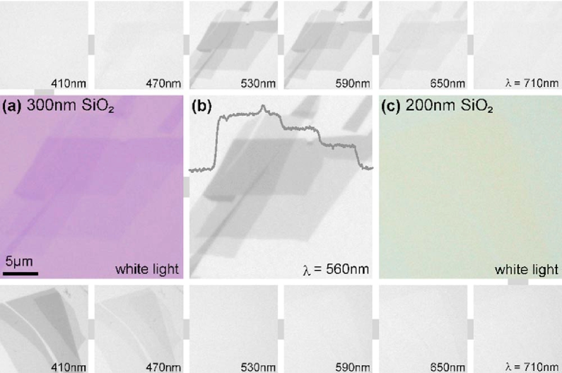
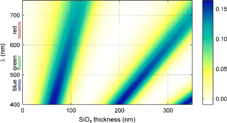
The identification of the “exfoliated graphene” on Si/SiO2 substrates by the group at the Manchester University [6] is one of the unquestionable milestone in the development of the graphene oriented research. Initially, however, it was perhaps not so clear why a few- or even single-graphene sheets can be seen just through an optical microscope. The explanation of this today widely accepted and frequently used experience is not trivial and invokes the importance of the spectroscopic analysis already at the birth of the graphene physics. As more recently revealed in details [37, 38, 39, 40, 41], the choice of the appropriate thickness of the SiO2 layer plays the essential role in the visualization of the graphene layers. As shown in Fig. 1, the contrast which is necessary to “see” the individual graphene layers depends on the wavelength of light and the actual thickness of the SiO2 layer. This is accounted by the analysis of multireflections from the sandwiched graphene/SiO2/Si structure within the framework of standard Fresnel equations (despite the fact that we are dealing with the material at the atomic resolution). The substrates used by Manchester group were characterized by 300-nm-thick oxide layers, for which the optimum contrast to see the graphene flakes is 10 % and falls in the middle of the visible range. This greatly helped to visualize the graphene flakes.
3 Graphene
3.1 Electronic band structure
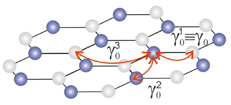
The first calculation of electronic states in a 2D lattice of carbon atoms with a honeycomb symmetry, see Fig. 2, dates back to 1947, when Wallace [5] used graphene as a starting element for description of bands in bulk graphite. Taking into account the strong hybridization of orbitals in the graphene plane, Wallace considered just the remaining orbital (oriented perpendicular to the crystal plane) to be responsible for the electronic band structure in the vicinity of the Fermi level and suggested a standard tight-binding approach. Considering only the nearest-neighbour hopping parameter (see Fig. 2), one easily finds a pair of -bands [2]:
| (1) | |||||
which distinctly cross (touch) at two inequivalent and points of the Brillouin zone, see Fig. 3. The strength of the nearest-neighbour hopping is eV [43] and the lattice constant nm [42] is by a factor of larger than the distance between the nearest carbon atoms.
In pristine graphene, the Fermi level lies just at the touching (crossing) point of and bands and graphene has a character of zero-band-gap semiconductor (semimetal). Close to a given crossing (touching) point, known also as the Dirac or charge neutrality point, the electronic bands are nearly linear and practically rotationally symmetric. In other words, the carrier dispersion relations take a simple form: , where the momentum is measured with respect to () point. The parameter , having dimension of a velocity, is directly related to the coupling strength (hopping integral) between the nearest carbon atoms: [2].

The linearity of bands in graphene (in the vicinity of the and points) implies that charge carriers in this material behave as relativistic particles with zero rest mass and constant velocity m.s-1. They are often referred to as massless Dirac fermions, and with a good precision, their behaviour is described by the effective Hamiltonian [2, 44]:
| (2) |
which is equivalent to the Hamiltonian in the Weyl equation for real relativistic particles with zero rest mass (originally for neutrinos) derived from the Dirac equation. Due to this formal similarity, a direct link between quantum electrodynamics and the physics of graphene is established.
The characteristic linear dispersion relations of electronic states makes graphene very distinct among other 2D systems (such as quantum wells or heterojunctions) which have been widely investigated in condensed-matter physics for last thirty years. For instance, the density of states in graphene is not constant as for conventional massive particles, , but rises linearly with the energy distance from the Dirac point: . Here, stand for the spin and valley degeneracies, respectively.
Nevertheless, it should be noticed that the relativistic-like image of electronic states in graphene given by Hamiltonian (2) remains an approximate model. This simple approximation is well, and perhaps even surprisingly well fulfilled in case of electronic states in the vicinity of the Dirac point. Those states indeed show almost perfect character of massless Dirac fermions when probed with different experiments. However, as can be seen from Fig. 3, the deviations from this relativistic model become obviously important for states far away from the Dirac point, even if we consider only the nearest neighbours in the tight-binding calculation. Other complications may arise when including the hopping integrals between further located neighbours. For example, when taking into account the non-zero values of hopping integrals [45, 46] (see Fig. 2), the nonlinearity is enhanced and Dirac cones become asymmetric with respect to the charge neutrality point [47, 46, 48].
3.2 Optical conductivity at
Interaction of massless Dirac fermions in graphene with light, expressed usually in terms of dynamical (optical) conductivity, has been theoretically treated at different levels of approximation [50, 51, 44, 52, 53, 54, 55, 56, 46, 57, 58, 59]. Within the simplest approach of electronic states described by Hamiltonian (2), only vertical in -space transitions across the Dirac point are optically active. Then, the dynamical conductivity takes a constant (energy independent) value of , which results in frequency-independent absorption of %, where (in cgs units) is the fine structure constant. Hence, in this model, the absorption of light in graphene is so-called universal, given just by which in general describes the strength of interaction between light and matter. Let us note that the graphene dynamical conductivity related to the vertical across the Dirac point transitions is frequency independent, , simply because the joint density of states is linear with energy (frequency). When considering the linearly polarized light, the contribution of individual -conserving transitions to the total optical conductivity depends on the angle between the given momentum and the vector of light polarization [51], but the universal conductivity is restored after integration over all angles.
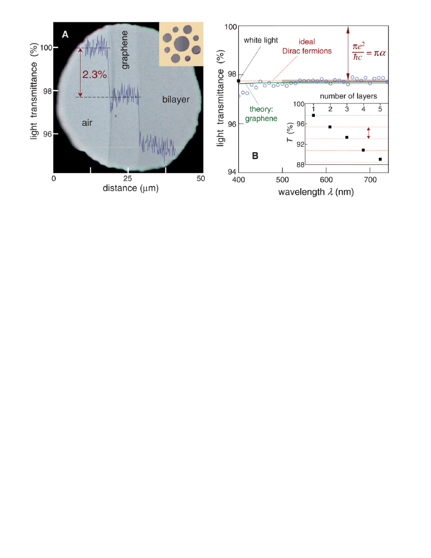
Transforming into measurable quantities, such as the optical transmission and reflection , one finds that ( [46]), and therefore, the absorption of light in graphene, and also the fine structure constant itself, can be estimated in a straightforward transmission experiment, . This fact was confirmed in recent experiments in the visible range on the self-standing graphene membrane [49], see Fig. 4, and further explored by other groups [60, 61]. The universality of the optical conductivity in graphene has been also discussed in the context of epitaxial graphene on SiC substrate [62] in a wide range of photon energies.
Nevertheless, we should mention that the declared universality of the graphene absorption is only approximative (what unfortunately limits its applications in metrology), since Hamiltonian (2) represents just the simplest model of the graphene band structure and therefore neglects the non-linearity of bands at high energy distance from the Dirac point. In other words, the absorption of light in graphene is as “universal” as “ideal” are massless Dirac fermions in this system. A theoretical analysis of these corrections was performed by Stauber et al. [46], who discussed not only deviations from non-linearity due to finite width of -bands as given by Eq. (3.1), but also included the effects of next-nearest hopping integral , see Fig. 2. Experimentally, the deviations of the optical conductivity from the “universal” value , have been probed in the visible range by Fei and coworkers [61]. Another departure from “universality” of the graphene transmission is provided by saturation effects, due to which graphene can find its use as a saturable absorber [63, 64, 65, 66].
It is worth noticing that a nearly universal conductivity has been also reported by Kuzmenko et al. [67] for bulk graphite (conductivity per single atomic sheet). Naively, one can seek for the origin of this effect in a relatively weak inter-layer coupling in graphite, but a deeper theoretical analysis is also available: the appearance of the universal conductivity (again per sheet) in multi-layer graphene stacks has been considered by Min and MacDonald [68] in relation to the presence of the chiral symmetry in structures with AB and/or ABC stacking sequences.
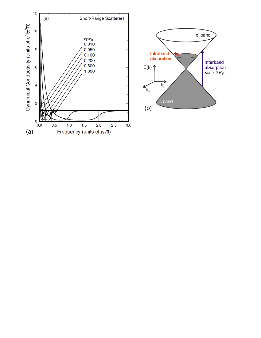
A more general theoretical approach to the optical conductivity of graphene, which includes the effects of carrier density, temperature, as well as carrier scattering (both short- and long-range scatterers considered), has been presented already in “pre-graphene” era by Ando et al. [50] in the framework of the self-consistent Born approximation, see Fig. 5a. Later on, further calculations were performed by Peres et al. [44] as well as Stauber et al. [57]. A simple analytical expression for the optical conductivity was found by Gusynin et al. [52] followed by Falkovsky and Varlamov [55]. These works account for both inter-band transitions which are blocked at energies below twice the Fermi energy () as well as intra-band transitions which result in the appearance of the Drude peak centered at zero frequency (see Fig. 5). As can be expected, these models uncover the universal conductivity in the limit of high energies. If the Fermi energy approaches the neutrality point, the optical conductivity is universally at any finite frequency but singular at . The apparent value of related to the so-called minimum conductivity is one of the lively discussed issue in the graphene physics, without clear consensus between different experiments and theoretical models so far [50, 3, 4, 30, 70, 71, 31].
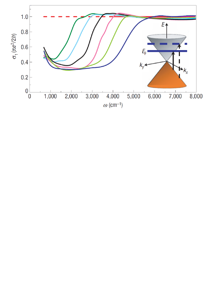
Experimentally, the optical response of exfoliated graphene flakes placed on Si/SiO2 substrates has been investigated in the mid-infrared range in the reflection configuration by Wang et al. [72] who reported the pronounced modification of graphene’s optical properties as a function of the position of the Fermi level. Further experimental data taken in both reflection and transmission mode, accompanied by a detailed analysis have been presented by Li et al. [69] and later on also by Mak et al. [60]. The spectrum of the optical conductivity extracted from these experiments (see Fig. 6) is in overall agreement with theoretical predictions. However, some of the observed features, such as the striking scaling of the onset of inter-band transitions with the gate voltage or the intriguing finite absorption in between the Drude peak and the onset remain to be firmly clarified. Possibly, these observations might be due to effects of disorder and/or of electron-electron interactions, which as yet may not be fully accounted in theoretical models [53].
3.3 Magneto-spectroscopy
-
Quantity Relations Numerical values Effective mass Density of states cm-2.meV-1 Carrier density cm-2 Energy of 1st LL meV
Cyclotron motion of charge carriers and the related cyclotron resonance phenomenon (absorption of light at cyclotron frequency ) is primarily a classical effect, probably the most representative for the magneto-optical spectroscopy. Such motion is not only characteristic for a conventional charged () particle with mass , which precesses with the frequency of . The solution of the classical equation of motion for charged particle with energy , depending linearly on momentum (), also results in the cyclotron motion but with the frequency , in which one easily identifies the energy dependent mass . This latter equation, equivalent to the Einstein relation between mass and energy, invokes again the relativistic-like character of electronic states in graphene. Perhaps surprisingly, the strictly speaking classical, i.e., linear with the magnetic field, cyclotron resonance has not been clearly observed in graphene so far, thought the existing experimental results are well explained by quantum mechanical approach.
In a quantum-mechanical picture, the application of the magnetic field perpendicular to the graphene plane transforms the continuous electronic spectrum into discrete and highly degenerate Landau levels (LLs) [73]:
| (3) |
whose positions are defined by a single material parameter, the Fermi velocity (). The degeneracy of each Landau level is , where we take into account both spin and valley degeneracies. This LL spectrum consists of electron levels (), hole levels () and the zero LL () which is shared by both types of carriers and which is responsible for the unusual sequence of the quantum Hall effect in graphene [3, 4]. We also immediately see that LLs in graphene are non-equidistant and they evolve as , see Fig. 7a, what both can be understood as a consequence of the extreme non-parabolicity (in fact linearity) of the bands. The unusual -dependence of LLs in graphene is responsible for its surprising sensitivity to the magnetic field. Experimentally, the well-defined LLs have been spotted in this system down to 1 mT and almost up to temperature of liquid nitrogen [74]. It might be realistic that Landau level quantization in pure graphene could also be observable in the magnetic field of the Earth ( T), which is unique for a condensed-matter system.
Interaction of light with graphene in a quantising magnetic field has been explored several times both theoretically and experimentally over the few past years [44, 75, 76, 77, 78, 79, 80, 81, 48, 47, 82, 74, 83]. To describe the magneto-optical response of graphene, we start with a single-particle model and use the Kubo-Greenwood formula [84, 85, 86]. Then, the longitudinal conductivity takes the following form:
| (4) |
where stands for the occupation of the -th LL and is a phenomenological broadening parameter. The matrix elements of the velocity operators and are and , respectively, with if or equals zero, and otherwise [76, 81, 79, 87].
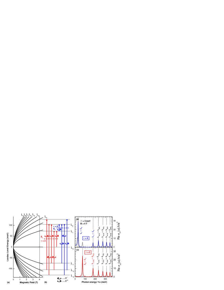
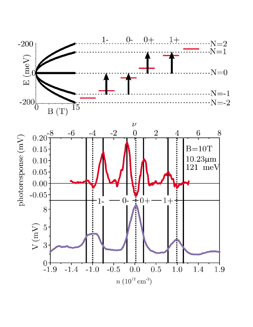
We see that graphene exhibits a relatively rich (multi-mode) magneto-optical response, where energies of individual resonances which correspond to individual inter-LL transitions scale as , preserving this unique property of the Landau level fan chart in graphene. Let us now discuss a few basic facts which imply from Eq. (4): All dipole-allowed inter-LL transitions in graphene follow the selection rules and , which are active in the and polarization of the incoming light [81, 87], respectively. The possible transitions can be divided into three groups (): Inter-band resonances and at energy , intra-band resonances and with energy and the mixed L L0(1) resonance, involving the LL, having energy of . From a purely terminological point of view, only intra-band resonances can be referred to as cyclotron resonance (CR), nevertheless, the term Cyclotron resonance experiments is used frequently to describe any of inter- or intra-band inter-LL transitions in the current literature, and becomes thus equivalent to a more general term of Landau level spectroscopy.
A scheme of optically active transitions for a hypothetical system of 2D Dirac fermions at two, arbitrary chosen, filling factors and 6 is illustrated in Fig. 7b. The corresponding optical-conductivity spectra are presented in Figs. 7c and 7d. The intra-band transitions appear at low energies and are followed by inter-band resonances at higher energies. There is however no distinct separation between these two types of transitions, what is in contrast to the case of conventional 2D systems based on gapped semiconductors, but somehow similar to the case of narrow-gap II/VI compounds structures [88, 89]. Nevertheless, in graphene, we deal with only one type of atomic orbital, and therefore both intra- and inter-band transitions follow similar selection rules: modulus of the LL index is changed by 1. This is again in contrast to the case of convectional 2D system, made for instance of GaAs, for which the inter-band transitions conserve the LL index and their dipole moment is due to different - and -orbitals of the conduction and valence band, respectively. Owing to the electron-hole symmetry of the graphene band structure, two different inter-band resonances, such as, for example and in Fig. 7b, may appear at the same energy. Such degenerated in energy transitions are however active in opposite circular polarization of light. At low temperatures one may expect at most two different intra-band transitions but a series of inter-band transitions. The situation is even more complex at higher temperatures, when the thermal spreading of the Fermi distribution exceeds the separation between Landau levels. The intra-band absorption (CR) may then also reveal a multi-mode character, as seen, for example, in Fig. 7d, where the grey curve depicts the thermal activation of LL1 and LL3 transitions. Such multi-mode intra-band absorption spectrum, which envelop corresponds, nota bene, to the classical cyclotron resonance discussed at the beginning of this section, was recently observed in graphene (on the surface of bulk graphite) by Neugebauer et al. [74].
Another interesting point is that the velocity operators (and also their matrix elements) are magnetic-field-independent in graphene, contrary to the case of standard systems with a parabolic band [90]. In consequence, if the occupation difference between the initial and final state Landau levels is not changed with the magnetic field (which is often the case of inter-band transitions), the oscillator strength of such a transition rises as , see Eq. (4) with . The transitions involving the Landau level are also interesting in this respect. In the quantum limit, once the Fermi energy is pinned to the level, the oscillator strength of the degenerate (non-polarized) L L0(1) transition does not depend on the particular occupation of this level. This is due to the fact that the change in one of the occupation factors () and () relevant for the L L0 and L L1 transitions, respectively, is compensated by the same gain for the other one. For the same reason, the oscillator strength of the unpolarized transition involving the LL increases as a at high magnetic fields. This is very much in contrast to the case of conventional electron gas with parabolic dispersion relations, for which the oscillator strength of the cyclotron resonance is just a measure of the electron concentration, including the high-field limit. However, the doping of graphene in this limit can still be deduced from the comparison of the intensities of the (polarized) L L1 and L L0 transitions.
-
Graphene specimen (106 m.s-1) (eV) Remark Exfoliated, SiO2 substrate 1.12 3.46 MO [78] Exfoliated, SiO2 substrate 1.09 3.37 MO [48] Epitaxial (C-terminated surface) 1.02-1.03 3.15-3.18 MO [76, 82] Epitaxial (C-terminated surface) 1.13 3.49 STS [29] Epitaxial (C-terminated surface) 1.0 3.1 ARPES [91] Decoupled on surface of bulk graphite 1.00 3.09 MO [74] Decoupled on surface of bulk graphite 0.79 2.4 STS [28]
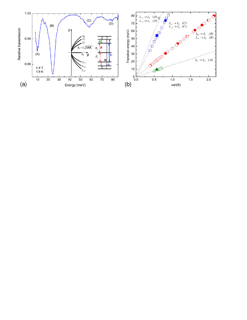
Experiments: Magneto-optical measurements, mainly magneto-transmission, have been up to now performed on three different kinds of graphene samples. First experiments were carried out on epitaxial graphene prepared by the thermal decomposition of the surface of silicon carbide [76, 80], see Fig. 8. To be more specific, these CR data have been obtained on a multilayer epitaxial graphene (MEG) specimen prepared on C-terminated surface of 4H-SiC. The Dirac-like spectrum, genuine of the graphene monolayer, found to dominate in MEG structures, has been initially an intriguing observation but this is today a well-established experimental fact [29, 91]. The electronic bands in MEG grown on the carbon face of SiC are alike those of a single layer because of preferentially rotational and not Bernal-type layer stacking in this material [92, 91]. To our knowledge, no reliable magneto-optical measurements have been reported on samples grown on Si-face of 4H-SiC (or 6H-SiC), where mostly the standard (well-known from bulk graphite) Bernal stacking is set. On the other hand, Si-face samples have been used in a number of ARPES experiments, see e.g. [23, 24, 25]. The magneto-optical experiments on epitaxial samples were soon followed by measurements on a single flake of exfoliated graphene [78, 48], see Fig. 9, and recently, also by CR in decoupled graphene sheets on the surface of bulk graphite [74]. To compare, whereas the large-size samples (up to a few mm2) covered with MEG flakes (up to a few mm2) allow for the relatively easy and precise CR measurements on well-defined, practically undoped graphene sheets ( cm-2 [82]), the demanding experiments on single flakes of exfoliated graphene are more subtle. They have been successfully realized with a differential (modulation) technique when using the gate voltage to tune the Fermi energy and therefore to block the apparent transitions in the reference signal. The magneto-transmission experiments offer several pieces of important information about electronic properties of graphene, we will summarize them in the following.
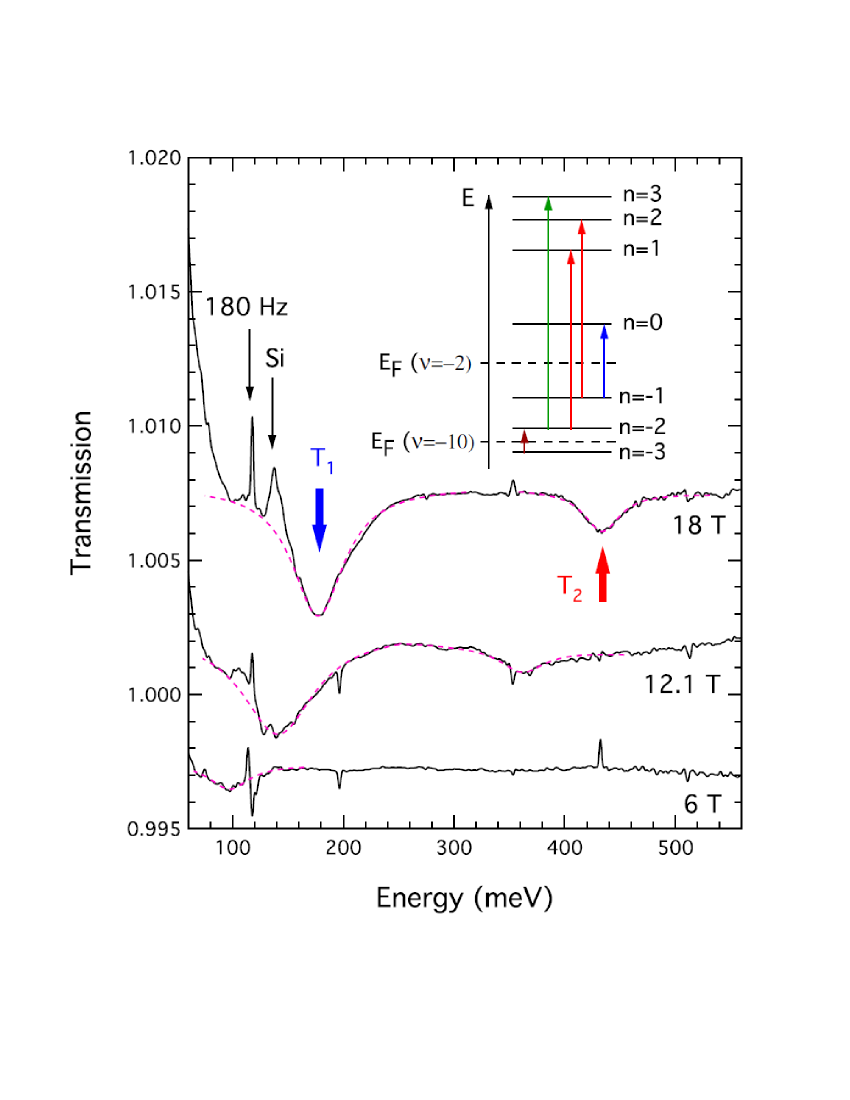
Landau level fan charts and Fermi velocity: A clear illustration of the characteristic scaling of Landau levels, in fact equivalent to the observation of linear dispersion relations of carriers, has been the first important feat of the Landau level spectroscopy of graphene systems [76]. Sadowski et al. [76] observed a practically perfectly -scaled Landau level fan chart in MEG structures and extracted m.s-1 for the Fermi velocity in this system. Jiang et al. [78] and subsequently Deacon et al. [48] found somehow higher values m.s-1 for gated (exfoliated) graphene flakes on Si/SiO2. We note that Landau levels in MEG structures as well as in graphene flakes floating on the graphite surface have been recently also visualized using tunnelling spectroscopy in magnetic fields [28, 29]. The Fermi velocity found in these later STS experiments agrees well with magneto-transmission data in case of MEG structures [76, 82] but it is surprisingly low m.s-1 [28] in case of graphene flakes on graphite, for which the magneto-spectroscopy gives much higher value of m.s-1 [74]. Individual values of the Fermi velocity determined in various samples by different experimental techniques have been summarized in Tab. 2.
Beyond simple band models: Relatively small but noticeably deviations of bands from their ideal linearity, of the order of a few percent at large eV distance from the Dirac point, have been found by a combination of far and near-infrared magneto-optical experiments performed on multi-layer epitaxial graphene by Plochocka et al. [47]. These deviations were revealed by a departure of the observed transitions from a simple -dependence, which rises with the photon energy of the probing light. No signs of the electron-hole asymmetry has been found in these experiments. On the other hand, the traces of the electron-hole asymmetry have been reported by Deacon et al. [48] in exfoliated graphene placed on Si/SiO2 substrate, who estimated the difference in the electron and hole Fermi velocities to be of the order of few percents. Magneto-transmission experiments if carried out on neutral graphene specimens may also bring a relevant information on a conceivable appearance of a gap at the Dirac point. Working in the limit of low magnetic fields, Orlita et al. have estimated a gap to be smaller than 1 meV in quasi-neutral MEG structures [82] and its maximum possible value of a fraction of 1 meV in graphene flakes on graphite substrates [74].
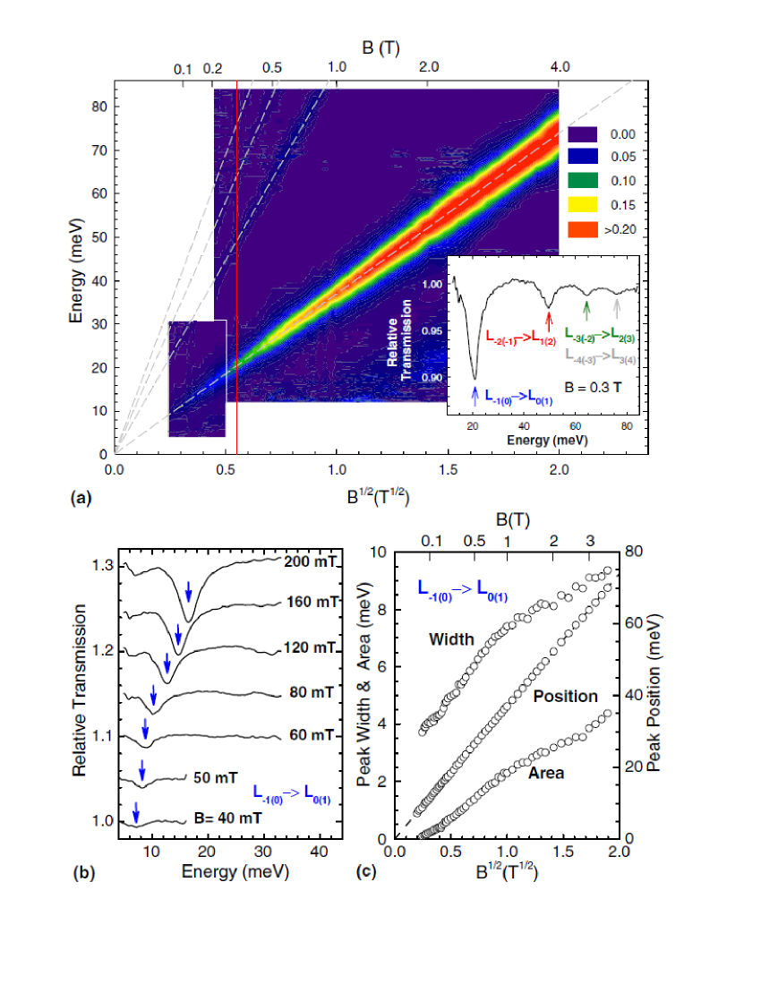
Scattering/disorder : Cyclotron resonance measurements on graphene, in particular in the limit of low magnetic fields (low frequencies) can be effectively used to estimate the scattering time and/or mobility of carriers. For instance, Orlita et al. [82] (working in fields down to 10 mT range) have shown (see Fig. 10) the possibility to achieve the room-temperature carrier mobility exceeding 250 000 cm2/(V.s), which is the record value among all other known materials. Recent predictions based on the analysis of transport data taken on exfoliated graphene [93] have been thus confirmed. Moreover, the closer look at the CR lineshape can offer valuable information about the scattering mechanisms. An increase of the (LL-independent) linewidth nearly following the -dependence indicates that the short-range scattering dominates in this particular case [94]. Using also the magneto-optical methods, the mobility of charged carriers exceeding cm2/(V.s) up to the temperature of liquid nitrogen has been determined for high-quality graphene flakes on the surface of bulk graphite [74]. CR measurements thus became a straightforward method to characterize the quality of graphene specimens, see, e.g., Ref. [95].
Electron-electron interaction: Since the discovery of graphene, the effects of electron-electron interaction were a subject of particular interest in this material. Nevertheless, a great majority of experimental results obtained on various graphene systems are fairly well understood within single particle models. This also concerns a number of magneto-transmission studies [76, 47, 82, 74]. Characteristically, they display a regular, defined by a single parameter series of transitions which are thus very tempting to be assigned as those between single particle Landau levels. However, the excitations between highly degenerate Landau levels are known as nontrivial processes which involve the effect of electron-electron interaction. Such an electron-hole excitation is characterized by its wavevector (nota bene proportional to electron-hole separation). The specific shapes of dispersion relations of inter and intra Landau level excitations are central for the many-body physics of the integer [96, 3, 4] and fractional [97, 98, 99] quantum Hall effects, respectively. We know from this physics that, when considering a single parabolic band of a conventional 2DEG (with equidistant Landau levels), the energies of optically active inter Landau level excitations correspond to those of single particle excitations. This can be viewed as a consequence of Kohn (or Larmor) theorem or seen as a result of perfect cancellation of Coulomb binding and a positive exchange term for the electron-hole excitation. This reasoning does not hold for a 2D gas of Dirac electrons, for which the exchange term may even largely exceed the Coulomb binding, both in addition expected to be different for different pairs of Landau levels. The apparent approximate validity of the Kohn theorem in graphene is a surprising effect, and in our opinion calls for further clarifications on the theoretical background. The first theoretical works dealing with this problem have been already published [100, 101, 102]. We note however here that although small but noticeable deviations from a perfect single particle scaling of inter Landau level excitations have been already reported in experiments on exfoliated graphene structures [78]. Very recently, Henriksen et al. [83] have reported changes in the energy of the L L0(1) transition, especially pronounced at high magnetic fields, when tuning the Fermi energy in between and Landau levels. Both these observations [78, 83] are discussed in terms of electron-electron interactions but perhaps also include some effects of disorder. Notably, magneto-optics allows for probing the nature of quasi neutral graphene in high magnetic fields (a possible appearance of a gap in the zero LL at filling factor zero), which recently became a subject of many theoretical considerations and experimental works [35, 103].
4 Bilayer graphene
4.1 Band structure
The interest in the physics of a graphene bilayer started after magneto-transport experiments of Novoselov et al. [20] who showed a characteristic quantum Hall effect and a Berry’s phase of with magneto-resistance measurements of this material. Carriers in a graphene bilayer are characterized by a finite mass but are clearly distinct from those in conventional systems with parabolic bands and referred to as massive Dirac fermions. Similarly to the case of graphene, the basics of the electronic band structure of the graphene bilayer have been established in 1947 by Wallace [5] and further developed in the band structure model of bulk graphite introduced by Slonczewski, Weiss and McClure [104, 105, 106] (SWM model). As a matter of fact, it is not graphene, but the graphene bilayer, which is the basic unit in the construction of Bernal-stacked bulk graphite.
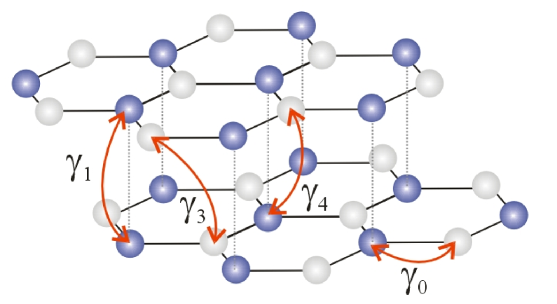
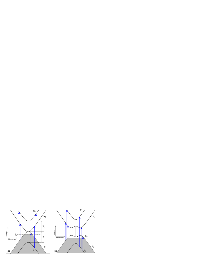
The presence of four atoms in the unit cell of the graphene bilayer implies the appearance of four bands in the vicinity of the Fermi level, instead of two in the graphene monolayer. The SWM model, reduced to a true bilayer, represents a solid basis for their description. This model implies one intra-layer and three inter-layer hopping integrals, see Fig. 11. In addition, the difference in on-site energies of stacked and unstacked triangular sublattices , as well as, the bias voltage applied across the layers are usually taken into account when modelling the band structure of the graphene bilayer.
As only , and parameters predominantly affect the shape of bands, we neglect the others for a while and express the Hamiltonian of the graphene bilayer as [21]:
| (5) |
which corresponds to the case of atoms in layers 1 and 2 ordered as . The electronic bands obtained by the diagonalization of this Hamiltonian have simple form of:
| (6) | |||||
These bands are symmetric with respect to the zero energy level, defined by the touching point of the bands and (so-called charged neutrality point) for , see Fig. 12a. A nearly parabolic shape of bands and close to the charge neutrality point allows us to introduce an effective mass with a relatively low value of [107] comparable to a mass found in narrow gap semiconductors. Assuming no doping or external gating, the Fermi level is located just at the charge neutrality point and similarly to graphene, the graphene bilayer can be viewed as a zero-gap semiconductor (semimetal). As sketched in Fig 12b, the external bias applied across the layers, transforms this gap-less band structure into a system characterised by a finite energy gap .
4.2 Optical conductivity at
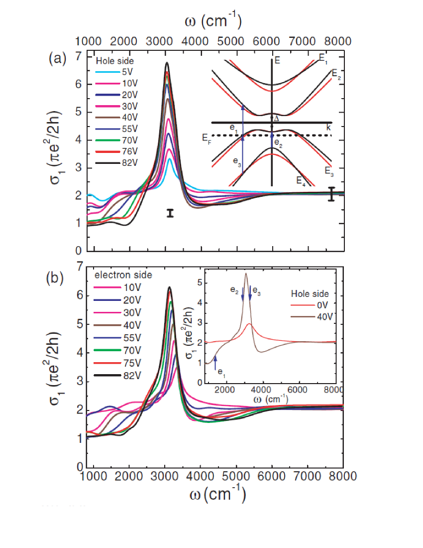
The relevant optical response of the graphene bilayer is expected in the infrared range, see the illustrative Fig. 12, as the characteristic band energy scale is given by the parameter eV [43]. Experiments have followed the well established theoretical background [87, 109, 110, 111, 112]. Two groups almost simultaneously reported on experiments performed on a single gated flakes of the exfoliated graphene bilayer [113, 108, 114, 115], see Fig. 13, overall confirming the expected electronic band structure given by Eq. (4.1). A more closer data analysis revealed a weak electron-hole asymmetry, going beyond the Hamiltonian (5) and quantified by parameters meV and meV [113], see also Tab. 4. No pronounced influence of the trigonal warping, expressed predominantly by the parameter, was found in these experiments. Very recently, analogous experiments have been performed on more sophisticated devices with two gates incorporated, allowing independent tuning of the carrier density and voltage [116, 117]. A possibility to smoothly tune the energy gap from zero up to meV has thus been demonstrated. The possibility of relatively easily tuning of the gap in the graphene bilayer depicts the interesting potential of this system in designing the electronic devices.
-
Quantity Relations Numerical values Effective mass 0.033 Density of states cm-2.meV-1 Carrier density cm-2 Cyclotron energy meV
4.3 Magneto-spectroscopy
In most of the experimentally studied cases, the graphene bilayer evokes the quantum mechanical character of its band structure under the magnetic field applied across the 2D plane. Following the Hamiltonian (5), the energy ladder of Landau levels with indices , is given by:
| (7) | |||||
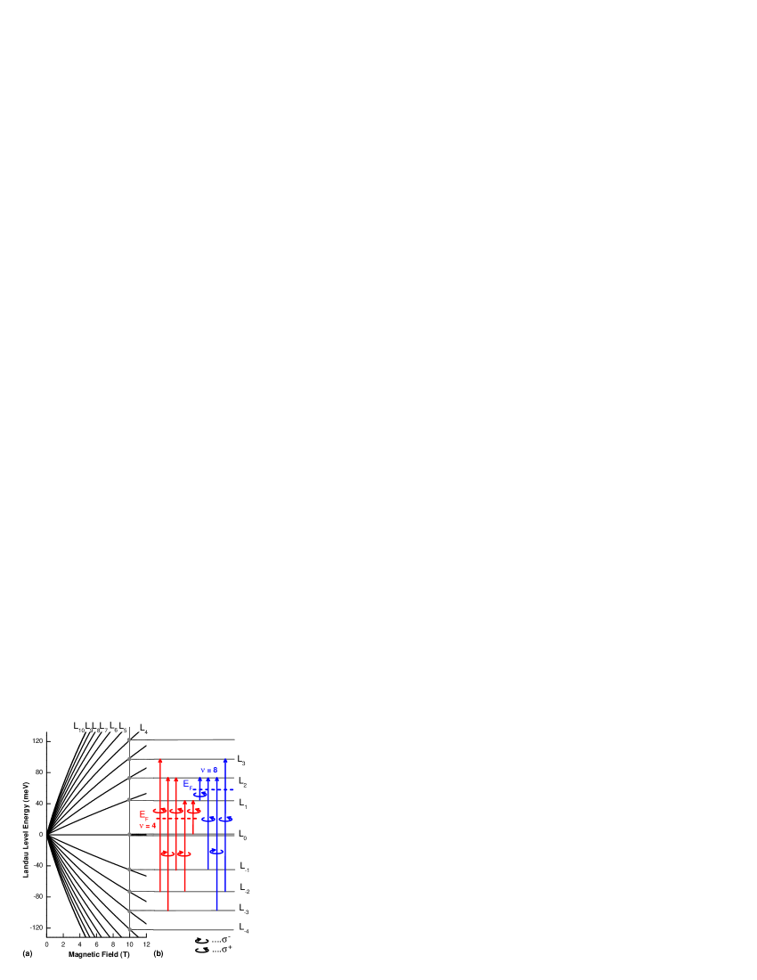
The eightfold () degeneracy of the LL with is twice the degeneracy of all other levels and this results in a characteristic quantum Hall effect with the Berry phase of [20, 21]. At energies around the neutrality point, the Landau levels are formed of and bands, and their energies are practically linear with . As shown in Fig. 14a, a departure from (saturation of) this linear dependence appears however at higher energy distances from the neutrality point (from the zero LL at energy zero) and/or for Landau levels with higher indices.
Similarly to the case of the graphene monolayer, the magneto-optical response of graphene bilayer can be described within the Kubo-Greenwood formalism, employed in the previous Chapter, but the individual matrix elements are not easy to evaluate. Up to now, this problem was approached approximatively by Mucha-Kruczyński et al. [118] and also some numerical results are available [119, 120]. In general, we expect that all transitions between LLs arising from all four bands are dipole-allowed, if the selection rules are obeyed, and they are active in the polarization of the incoming light, respectively. A few transitions in the vicinity of the Fermi level, including their polarization, are schematically shown in Fig. 14b, for two arbitrarily chosen filling factors and 8. Certain additional complications arise from the appearance of the trigonal warping, expressed mainly by the parameter , which is not included in the Hamiltonian (5) and which induces the second set of dipole-allowed transitions between LLs. Such transitions appearing between levels whose indices differ by , where [87], may have their oscillator strengths comparable with transitions but only at low magnetic fields [87].
The scheme of inter Landau level transitions in a graphene bilayer is largely simplified when a parabolic approximation of and bands is considered [21], i.e. when the Hamiltonian (5) is reduced to 22 matrix (the and split-of bands are neglected). This approach seems to be fairly sufficient when considering the low-energy excitations in an undoped or weakly doped graphene bilayer. The LL spectrum then takes the form of for , or equivalently:
| (8) |
where stands for the cyclotron frequency with . In this approximation, the Landau levels are perfectly linear with the applied field . Let us note that in the limit of high (practically even for ), the LL spectrum Eq. (8) has the form , typical of conventional massive particles.
Within the parabolic approximation, the matrix elements of the velocity operators, , to be set in the Kubo-Greenwood formula, have been evaluated by Abergel and Fal’ko [87]. They obtained: (for and ), where denotes the magnetic length. Transitions involving doubly degenerated LL level must be taken into separately. The spectrum is obviously expected to depend on the actual position of the Fermi energy and special care has to be taken to account for possible splitting of the Landau level (including the elucidation of the character of this splitting). To prevent confusion, we note that our convention of LL indexing differs from the one used by Abergel and Fal’ko, whose Landau level spectrum reads: for , as compared to our Eq. (8).
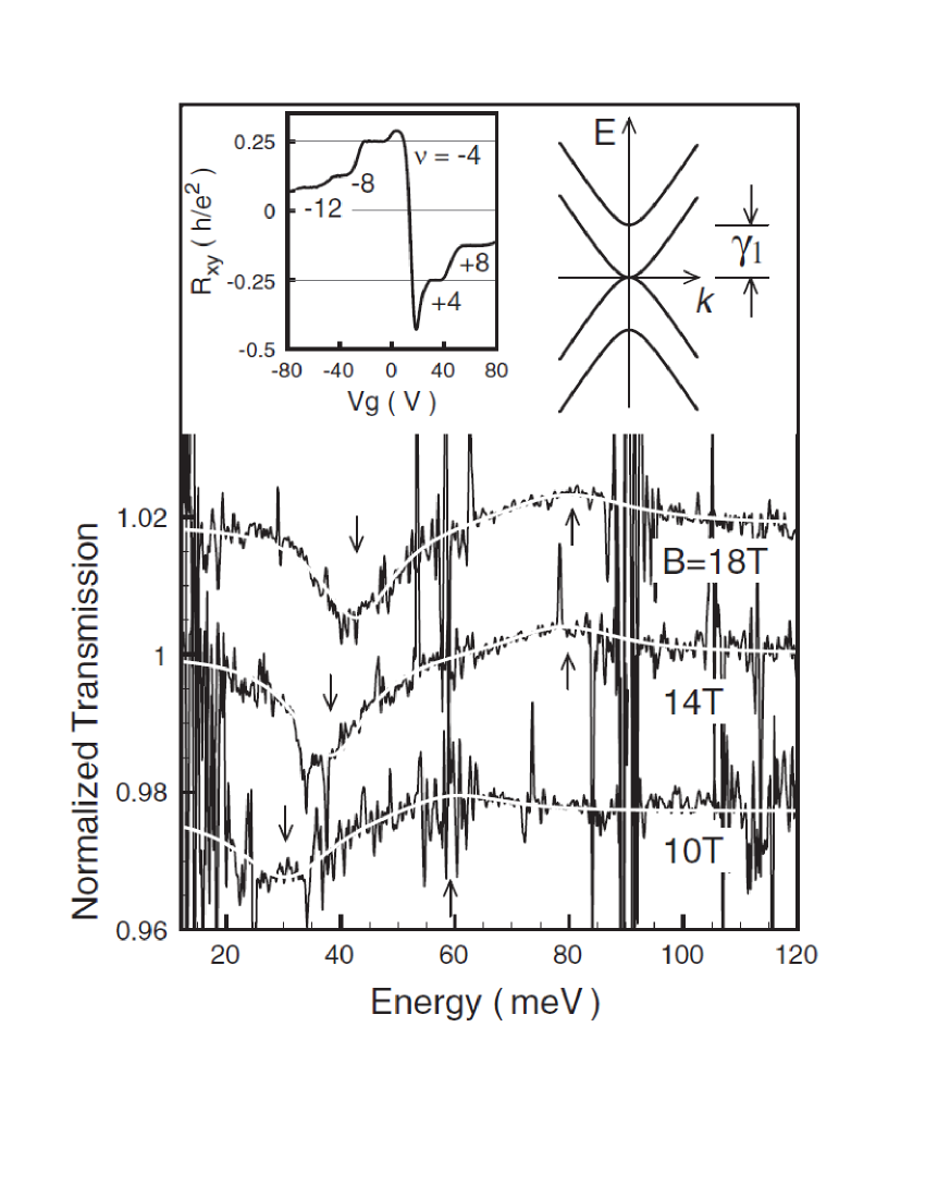
The available magneto-optical data on a graphene bilayer are not as rich as on graphene. Probably the only report is by Henriksen et al. [107], who examined a single gated flake of an exfoliated graphene bilayer in (differential) far infrared magneto-transmission experiments. In this work [107] the authors investigated the transitions between the adjacent LLs (intra-band transitions) as a function of the magnetic field and the carrier density (filling factor). A relatively good agreement with the simplified LL energy spectrum (4.3) has been obtained for low carrier densities. At higher filling factors, deviations appear due to the finite energy gap induced by the gate voltage, as recently explained by Mucha-Kruczyński et al. [121].
5 Graphite
5.1 Band structure
The renewed interest in the properties of bulk graphite is a direct consequence of the outbreak of the current graphene physics. As a 3D crystal, graphite is a system characterised by a higher degree of complexity compared to graphene, nevertheless, both material share many common properties.
The physics of bulk graphite has been reviewed several times, see e.g. Refs. [42, 43]. Here we mostly focus on optical properties which distinctly uncover the massless and massive Dirac-like electronic states also in this material. The appealing possibility to trace the “relativistic” carriers not only in graphene monolayer and bilayer, but also in bulk graphite (which is definitely easier to handle!) resulted in a number of works which offer new pieces of information, new interpretations of old data but often also rediscoveries of well-established knowledge.
Starting with the pioneering work of Wallace [5], the fundamentals of the graphite band structure have been formulated by Slonczewski, Weiss and McClure in fifties [105, 104, 106], as already mentioned in Section 4. This model describes the band structure along the -- line of the 3D Brillouin zone, see Fig. 16, which is responsible for most of the electrical and optical properties of bulk graphite. The SWM model mostly implies six hopping integrals , as sketched in Fig. 17, and additional parameter , usually referred to as pseudogap and related to the difference of the crystal field on atom-sites A and B. By definition, this pseudogap is related to a similar parameter in an isolated graphene bilayer as .
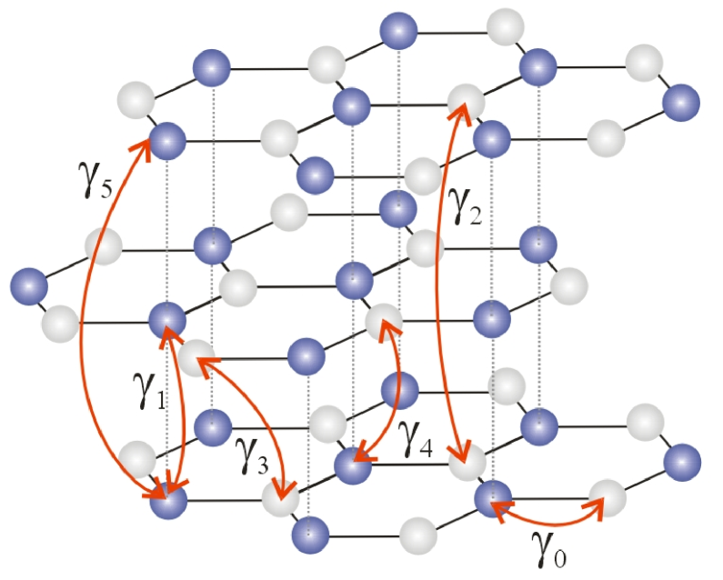
To describe optical response of graphite, we leave the full complexity of the SWM model and follow a simplified approach taking account only two most relevant hopping integrals and , which describe intra- and interlayer tunnelling, respectively [122, 119]. In this way, the band structure of bulk graphite along the -- is obtained by the diagonalization of the Hamiltonian:
| (9) |
which is formally equivalent to that of an unbiased graphene bilayer (5), with the same ordering of the atomic wavefunctions, but with an effective coupling tuned by the momentum in the direction perpendicular to layers, . The appearance of the cosine band in , having the amplitude of , thus reflects the periodic crystal ordering along the -axis, similarly to formation of minibands in semiconductor superlattices [123].
The straightforward diagonalization of the Hamiltonian (9) gives the band structure in the form of Eq. (4.1), i.e. electronic bands equivalent to the graphene bilayer, but with an effective coupling :
| (10) |
Hence, depending on their momentum along the -axis, electrons in bulk graphite behave as massive Dirac fermions in graphene bilayer, but with an effective coupling , which directly gives their effective mass . For example, electrons at the point () behave as massive Dirac fermions with an effective mass enhanced twice () in comparison to true graphene bilayer. Carriers (in real graphite holes) at the point () have a character of massless Dirac fermions due to the effectively vanishing inter-layer coupling (). Bulk graphite thus shares some common properties with the graphene monolayer as well as its bilayer.
5.2 Optical conductivity at
In reflection and/or transmission experiments at zero magnetic field the whole optical response corresponds to an average over all momenta along the -- line. With this averaging, the concluded response (per one sheet) is surprisingly close to the optical conductivity of an isolated graphene monolayer, as pointed out by Kuzmenko et al. [67], see also Refs. [125, 126]. Hence, a nearly universal optical conductivity can also be observed in bulk graphite.
5.3 Magneto-spectroscopy
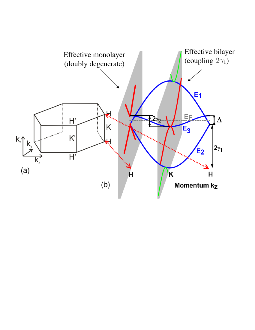
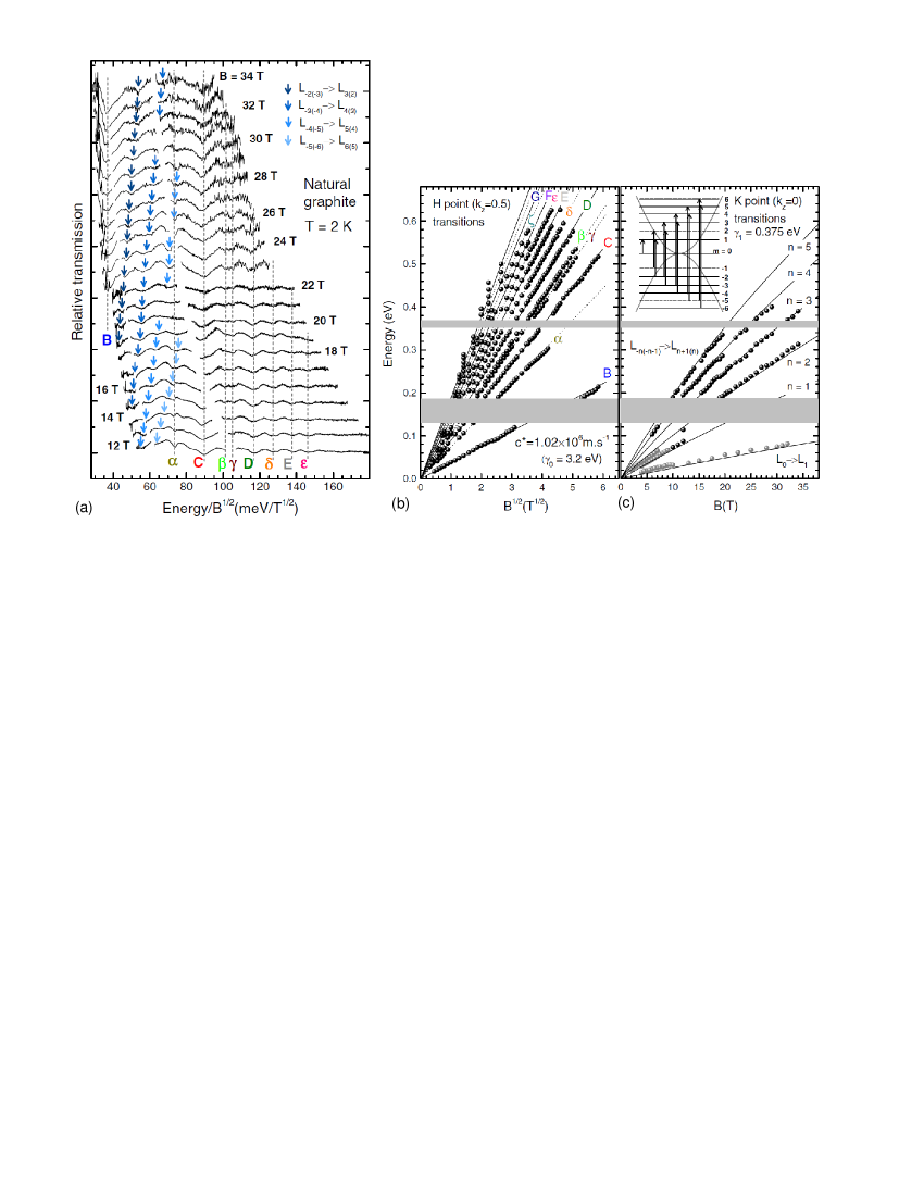
Historically, the verification of the band structure expected in the framework of the SWM model and estimates of individual tight-binding parameters have been often done using optical experiments in magnetic fields. In this case, the main contribution to the optical response is provided just by the and points, where Landau bands become flat, what leads to singularities in the joint density of states [119, 120]. Cyclotron resonance of massive electrons around the point was reported in several works, see older papers Refs. [127, 128, 129, 130] and also recent measurements [125], showing well-defined response which scales nearly linearly with . Much less information has been collected about the massless Dirac fermions around the point but nevertheless the features in magneto-reflection spectra which follow the -dependence, typical of 2D massless particles, have been already reported by Toy et al. [124]. This work [124] may be considered as probably a very first observation of massless Dirac fermions in solids. Later on, magneto-transmission experiments on a very thin graphite specimen (100 sheets) allowed for a deeper analysis of the point optical response [131, 132]. Magneto-optical response of the point of graphite includes a set of transitions equivalent to those of graphene [76, 78, 48], but it is nevertheless significantly richer [133]. Since there are four carbon atoms in the unit cell of graphite (and only two in the unit cell of graphene) the degeneracy of Landau levels in graphite (at the point only) is doubled as compared to the case of graphene. This results in a set of additional dipole allowed inter Landau transitions at the point of graphite which are indeed observed in experiments, see transitions marked with small Greek letters in Fig. 19.
The basic understanding of the complex magneto-optical response of bulk graphite [134], see Fig. 19, is possible just by viewing this material as an effective graphene monolayer and an effective bilayer with a coupling strength enhanced twice in comparison to a true graphene bilayer. Interestingly, this model including only two material parameters, and , is capable to catch the basic (magneto-)optical properties of bulk graphite, a complex 3D material. This creates an interesting link between physics of bulk graphite and graphene monolayer and bilayer. The values of band structure parameters determined by magneto-transmission experiments [134] are eV and meV. The presented model is however evidently simplified, and therefore, let us now consider the role of other tight-binding parameters and .
The integral , due to the hopping between next-nearest graphene planes (see Fig. 17), is dominantly responsible for the presence of electron and hole pockets around and points and therefore, i.e., for the semimetallic character of graphite. This is clearly evidenced for instance by magneto-transport experiments [135, 136, 137, 138]. Using the language of the effective graphene bilayer and monolayer, we obtain an effective -doped bilayer at the point with the Fermi level meV and similarly, -doped monolayer around the point with meV. It is important to note that magneto-optics and magneto-transport probes are sensitive to very different states selected from those along the - dispersion line. Magneto-optics is selective with respect to the states at and points, because it is sensitive to the maxima in joint density of states (integrated along the direction) of Landau bands which becomes flat at the extreme of the Brillouin zone along the direction. In turns, magneto-oscillations in transport or de Haas-van Alphen experiments result from the subsequent coincidences between the Fermi energy position and the maximum in the density of states. Those latter maxima appear not only at and point but importantly also at the intermediate point somewhere in the middle of the dispersive line. It appears that - and intermediate-point maxima, both reflecting rather massive (bilayer) character, are responsible for the two characteristic sequences of magneto-oscillations observed in magneto-transport experiments on graphite [139, 138, 140].
Trigonal warping of the band structure of graphite is described in the SWM model by the parameter ( meV [43]), and its relative influence on the band structure is scaled with the parameter [120]. Therefore, the band structure is mainly modified in the vicinity of the point and its influence at the point is completely cancelled. Probably, the most pronounced effect related to trigonal warping is the observation of the harmonics of the basic CR mode due to the -point electrons. Interestingly, parameter negligibly affects the LL energies at the point, but it induces new selection rules allowing transitions between LLs differing by in their indices [127, 141, 129, 130], whose relative strength is increasing with the decreasing magnetic field [87]. Let us note, however, that determination of LLs within the full SWM model is only possible via direct numerical diagonalization of a truncated infinite matrix [142].
The effects of and parameters are analogous to the the case of a true bilayer, i.e., they in principle induce the electron-hole asymmetry of the band structure as discussed in the previous Section. Again, the effective strength of scales with , giving the most pronounced effects at the point, where a relatively weak asymmetry has been observed [143, 144, 67, 134, 145]. At the point, the parameter corresponds to a (pseudo)gap opened at the Dirac point in the graphene-like band structure and is estimated in the range of several meV [124, 131, 45, 132].
6 Few-layer Bernal-stacked segments of graphite
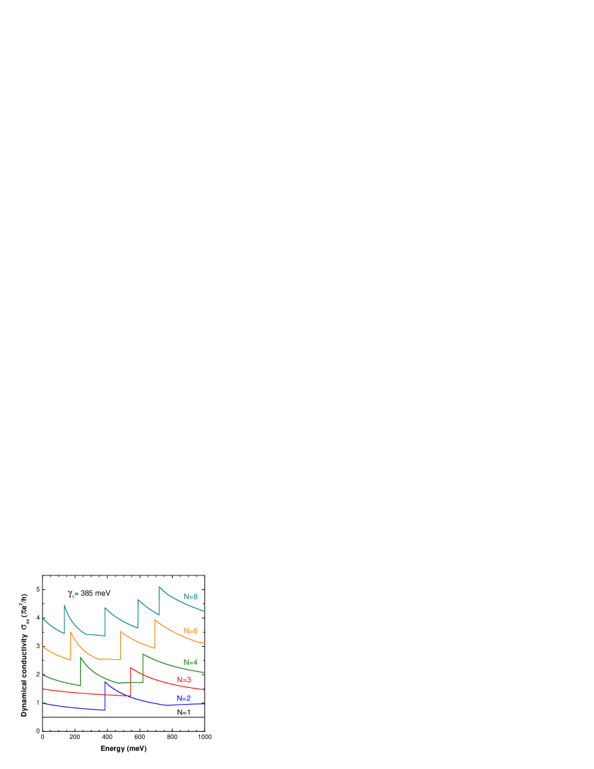
A fairly established knowledge about optical properties of the 2D graphene monolayer and bilayer, as well as 3D bulk graphite logically leads to a question about the properties of graphene stacks composed of three and more layers with Bernal ordering of sheets. As pointed out by Partoens and Peeters [146] the 10-layer graphene stack resembles already graphite very much, but the investigation of the graphene-to-graphite evolution is interesting and instructive. To get insight into the electronic states of a few-layer graphite stack, we use a relatively simple and intuitive model. We start with the electronic band structure of bulk graphite and select discrete values of momentum along the -axis, , with for odd or with for even , for which a standing wave appears in a stack with layers. Using a mathematical language, this approach corresponds to a decomposition of the Hamiltonian (assumption that is compulsory) describing a graphite stack with -layers (dimension ) into a set of sub-Hamiltonians (). For even , each segment corresponds to the Hamiltonian of the bilayer with the effective coupling constant , which is directly related to the allowed discrete values of momentum as . For odd number of stacked layers , we get very similar results, effective bilayers and one monolayer-like Hamiltonian (). Hence, in this way, the problem of the band structure of few-layer graphite is reduced to the already discussed band structures of graphene monolayer and bilayer, by simple introducing the appropriate effective coupling parameters. This approach has been discussed by Partoens and Peeters [122] and further developed by Koshino and Ando [147, 119, 120] who also included the influence of the magnetic field. Perhaps more elaborated, but less intuitive approach can be found, e.g., in Refs. [148, 45].
Experimentally, only very first measurements which probe the optical properties of graphene stacks with have just appeared for stacks up to . They display a clear evolution of the absorption spectra as a function of and well resemble the features which can be seen in the traces of the calculated optical conductivity, expected in these structures (see Fig. 20).
7 Summary and Outlook
Optical spectroscopy has in recent years been successfully applied to investigate the properties of new two dimensional allotropes of carbon and to revise the properties of bulk graphite. Majority of these experiments have been devoted to establish or verify the band structure character of the investigated materials and they certainly helped to establish and/or to better understand the characteristic nature of massless or massive Dirac electronic states in graphene [69, 78, 48, 49, 60], in graphene-like MEG layers on SiC [76, 47, 82], in bilayer graphene [113, 108, 114, 116, 117], or in graphite [131, 67, 134] and its few layer segments [149]. Characteristically for these semimetalic materials, the methods of infrared spectroscopy have been frequently used but also (nearly) visible optics appeared as a relevant tool to uncover their properties [49, 47, 61, 150]. The authors of this review are particularly attached to magneto-spectroscopy techniques and consider them among the most effective methods to studying the band structure parameters. Estimations of the Fermi velocity in graphene based systems or of the band curvature (effective mass) in bilayer graphene structures are the primary results of applications of these methods, see Tabs. 1–4. In complement to convectional electric transport measurements, the magneto-optics is also effective to evaluate the efficiency of carrier scattering [82, 95] and becomes a unique method if the electric contacts cannot be applied.
More challenging for experimentalists, such as the authors of this review, is to uncover the unexpected properties. Identification, with magneto-optical experiments, of graphene-like bands in MEG structures [76] was certainly a surprise, but is now a well acknowledged fact [92, 29, 91]. Similarly, the surprisingly extremely weak scattering efficiency anticipated for graphene from magneto-optical experiments [74] founds also its justification in a very recent theoretical work [151]. The deviations from simple models, tentatively attributed to the effects of electron-electron interactions, observed in the magneto-optical studies of graphene [78, 83] or in studies at [69, 60] are equally appealing.
It is obviously risky to foresee the further developments in optics of graphene-related structures but probably safe to say that they will be very much dependent on the progress in sample preparation: fabrication of easy handled large area samples, of systems with higher electronic quality and certainly new structures. Optical and magneto-optical methods will continue to be used to extract the relevant band structure parameters of these materials. These methods are likely to be of particular importance with respect to intense efforts of band gap engineering in different graphene systems [20] (e.g., graphene bilayer under the applied voltage [116, 117, 121, 115] or chemically functionalised graphene [152, 153, 154]). The problem of the specific, for linear bands, role of electron-electron interactions in inter Landau level transitions is to be clarified both on the experimental and theoretical ground. Better quality samples could certainly help in experiments, as they recently did in the case of the first observations of the fractional quantum Hall effect in graphene [98, 99]. Intriguingly, the classical collective phenomena such as low energy plasmons are absent in the experiments so far. This is to be verified, for example, in low-field low-frequency magneto-optical experiments on samples with well defined shape, as already done for standard 2D semiconductor systems [155, 156]. Low-energy plasma excitations might be very unique in graphene [157, 158, 159, 160, 161] and also interesting from the viewpoint of THz applications [162]. The predicted nonlinear effects related to cyclotron resonance and/or plasmon excitations are also to be examined [163, 164]. A possibility to detect the cyclotron resonance emission which may perhaps easily appear in the system with non-equidistant Landau levels, due expectable inefficient inter-Landau level Auger processes [165, 166, 167], is worth to verify. This could give rise to efficient ( tunable) sources of infrared radiation or even to THz lasers [168]. (Magneto-)optical experiments may be also decisive in confirmation of the Dirac subbands [169] when fabricating the artificial graphene [170] (by honeycomb lithography of a conventional 2DEG). Approaching the illusive quantum electrodynamics effect of Zitterbewegung is perhaps another challenge for optics of graphene [17, 171, 172, 173].
It should be stressed that this review covers only the basic linear transmission/reflection optical studies of graphene-based structures. For example, it does not include the vast domain of Raman scattering experiments [174, 175]. We just briefly note, that Raman scattering measurements on graphene systems are so far limited to investigations of the phonon response. However, since we deal with resonant processes, the phonon response also includes information on the electronic bands and, for example, its analysis has become one of the most popular method of primary characterization of different graphene structures. The electron-phonon interaction [176, 177] is another important issue that has been successfully studied in graphene using Raman scattering techniques [178, 179], including also the application of magnetic fields [180, 181, 182]. Observation of Raman scattering signal due to electronic excitations in graphene systems [183] would be highly interesting in view of investigations of single particle versus collective plasmon excitations and/or dispersion relations (due to electron-electron interaction) of inter Landau level excitations. Another class of optical experiments, which are not discussed here, concerns time resolved studies and the related investigations of carrier dynamics. There are already few reports in this area [184, 185, 186, 187, 167, 188, 189, 190], which is likely to expand in the future. Investigations of carrier dynamics with time resolved studies in the far infrared range and under application of a magnetic field might be interesting with respect to search for far infrared emission from graphene structures. One may finally speculate that these are perhaps the unexpected discoveries, such as the recent report on broad band emission from graphene in the visible range [150] (induced by oxygen plasma etching), which will open the entirely new domain in optics of two-dimensional allotropes of carbon.
8 Acknowledgements
This work has been supported by the European Commission via EuroMagNET II contract no. 228043 and Marie Curie Actions MTKD-CT-2005-029671 grant, as well as by PCR CNRS(France)-CNRC(Canada), CNRS-PICS-4340, MSM0021620834, KAN400100652, GACR no P204/10/1020 and Barrande no 19535NF projects.
9 References
† M. O. is also affiliated at the Institute of Physics, Charles
University in Prague, Czech Republic and Institute of Physics ASCR, v.v.i.,
Prague, Czech Republic.
References
- [1] A. K. Geim and K. S. Novoselov. The rise of graphene. Nature Mater., 6:183, 2007.
- [2] A. H. Castro Neto, F. Guinea, N. M. R. Peres, K. S. Novoselov, and A. K. Geim. The electronic properties of graphene. Rev. Mod. Phys., 81:109, 2009.
- [3] K. S. Novoselov, A. K. Geim, S. V. Morozov, D. Jiang, M. I. Katsnelson, I. V. Grigorieva, S. V. Dubonos, and A. A. Firsov. Two-dimensional gas of massless dirac fermions in graphene. Nature, 438:197, 2005.
- [4] Y. B. Zhang, Y. W. Tan, H. L. Stormer, and P. Kim. Experimental observation of the quantum hall effect and berry s phase in graphene. Nature, 438:201, 2005.
- [5] P. R. Wallace. The band theory of graphite. Phys. Rev., 71:622–634, 1947.
- [6] K. S. Novoselov, A. K. Geim, S.V. Morozov, D. Jiang, M. I. Katsnelson, I.V. Grigorieva, S.V. Dubonos, and A. A. Firsov. Electric field effect in atomically thin carbon films. Science, 306:666, 2004.
- [7] C. Berger, Z. Song, T. Li, X. Li, A. Y. Ogbazghi, R. Feng, Z. Dai, A. N. Marchenkov, E. H. Conrad, P. N. First, and W. A. de Heer. Ultrathin epitaxial graphite: 2d electron gas properties and a route toward graphene-based nanoelectronics. J. Phys. Chem. B, 108:19912, 2004.
- [8] C. Berger, Z. Song, X. Li, X. Wu, N. Brown, C. Naud, D. Mayou, T. Li, J. Hass, A. N. Marchenkov, E. H. Conrad, P. N. First, and W. A. de Heer. Electronic confinement and coherence in patterned epitaxial graphene. Science, 312:1191, 2006.
- [9] J.-I. Flege P. W. Sutter and E. A. Sutter. Epitaxial graphene on ruthenium. Nature Mater., 7:406, 2008.
- [10] A. L. Vázquez de Parga, F. Calleja, B. Borca, Jr. M. C. G. Passeggi, J. J. Hinarejos, F. Guinea, and R. Miranda. Periodically rippled graphene: Growth and spatially resolved electronic structure. Phys. Rev. Lett., 100:056807, 2008.
- [11] A. Grüneis and D. V. Vyalikh. Tunable hybridization between electronic states of graphene and a metal surface. Phys. Rev. B, 77:193401, 2008.
- [12] K. S. Kim, Y. Zhao, H. Jang, S. Y. Lee, J. M. Kim, K. S. Kim, J.-H. Ahn, P. Kim, J.-Y. Choi, and B. H. Hong. Large-scale pattern growth of graphene films for stretchable transparent electrodes. Nature, 457:706–710, 2009.
- [13] Alexander Gruneis, Kurt Kummer, and Denis V Vyalikh. Dynamics of graphene growth on a metal surface: a time-dependent photoemission study. New J. Phys., 11:073050, 2009.
- [14] Xuesong Li, Weiwei Cai, Jinho An, Seyoung Kim, Junghyo Nah, Dongxing Yang, Richard Piner, Aruna Velamakanni, Inhwa Jung, Emanuel Tutuc, Sanjay K. Banerjee, Luigi Colombo, and Rodney S. Ruoff. Large-Area Synthesis of High-Quality and Uniform Graphene Films on Copper Foils. Science, 324(5932):1312–1314, 2009.
- [15] A. K. Geim. Graphene: Status and Prospects. Science, 324:1530–1534, 2009.
- [16] M. I. Katsnelson, K. S. Novoselov, and A. K. Geim. Chiral tunnelling and the klein paradox in graphene. Nature Phys., 2:620–625, 2006.
- [17] M. I. Katsnelson. Zitterbewegung, chirality, and minimal conductivity in graphene. Eur. Phys. J. B, 51:157, 2006.
- [18] C. W. J. Beenakker. Colloquium: Andreev reflection and klein tunneling in graphene. Rev. Mod. Phys., 80:1337, 2008.
- [19] A. F. Young and P. Kim. Quantum interference and klein tunnelling in graphene heterojunctions. Nature Phys., 5:222–226, 2009.
- [20] K. S. Novoselov, E. McCann, S. V. Morozov, V. I. Fal’ko, K. I. Katsnelson, U. Zeitler, D. Jiang, F. Schedin, and A. K. Geim. Unconventional quantum Hall effect and Berry’s phase of 2 in bilayer graphene. Nature Phys., 2:177–180, 2006.
- [21] E. McCann and V. I. Fal’ko. Landau-level degeneracy and quantum hall effect in a graphite bilayer. Phys. Rev. Lett., 96:086805, 2006.
- [22] M. F. Craciun, S. Russo, M. Yamamoto, J. B. Oostinga, A. F. Morpurgo, and S. Tarucha. Trilayer graphene is a semimetal with a gate-tunable band overlap. Nature Nanotech., 4:383, 2009.
- [23] T. Ohta, A. Bostwick, T. Seyller, K. Horn, and E. Rotenberg. Controlling the Electronic Structure of Bilayer Graphene. Science, 313:951–954, 2006.
- [24] A. Bostwick, T. Ohta, T Seyller, K. Horn, and E. Rotenberg. Quasiparticle dynamics in graphene. Nature Phys., 3:36–40, 2007.
- [25] S. Y. Zhou, G.-H. Gweon, A. V. Fedorov, P. N. First, W. A. de Heer, D.-H. Lee, F. Guinea, A. H. Castro Neto, and A. Lanzara. Substrate-induced bandgap opening in epitaxial graphene. Nature Mater., 6:770–775, 2007.
- [26] A. Grüneis, C. Attaccalite, T. Pichler, V. Zabolotnyy, H. Shiozawa, S. L. Molodtsov, D. Inosov, A. Koitzsch, M. Knupfer, J. Schiessling, R. Follath, R. Weber, P. Rudolf, L. Wirtz, and A. Rubio. Electron-electron correlation in graphite: A combined angle-resolved photoemission and first-principles study. Phys. Rev. Lett, 100:037601, 2008.
- [27] J. Martin, N. Akerman, G. Ulbricht, T. Lohmann, J. H. Smet, K. von Klitzing, and A. Yacoby. Observation of electron -hole puddles in graphene using a scanning single-electron transistor. Nature Phys., 4:144, 2008.
- [28] G. Li, A. Luican, and E. Y. Andrei. Scanning tunneling spectroscopy of graphene on graphite. Phys. Rev. Lett., 102:176804, 2009.
- [29] D. L. Miller, K. D. Kubista, G. M. Rutter, M. Ruan, W. A. de Heer, P. N. First, and J. A. Stroscio. Observing the Quantization of Zero Mass Carriers in Graphene. Science, 324:924–927, 2009.
- [30] Y.-W. Tan, Y. Zhang, K. Bolotin, Y. Zhao, S. Adam, E. H. Hwang, S. Das Sarma, H. L. Stormer, and P. Kim. Measurement of scattering rate and minimum conductivity in graphene. Phys. Rev. Lett., 99:246803, 2007.
- [31] J.-H. Chen, C. Jang, S. Adam, M. S. Fuhrer, E. D. Williams, and M. Ishigami. Charged-impurity scattering in graphene. Nature Phys., 4:377, 2008.
- [32] P. Blake, R. Yang, S.V. Morozov, F. Schedin, L.A. Ponomarenko, A.A. Zhukov, R.R. Nair, I.V. Grigorieva, K.S. Novoselov, and A.K. Geim. Influence of metal contacts and charge inhomogeneity on transport properties of graphene near the neutrality point. Solid State Commun., 149:1068 – 1071, 2009. Recent Progress in Graphene Studies.
- [33] A. K. Geim and A. H. MacDonald. Graphene: Exploring carbon flatland. Phys. Today, 60:35–41, 2007.
- [34] V. Gusynin, S. Sharapov, and J. Carbotte. Ac conductivity of graphene: from tight-binding model to 2+1 dimensional quantum electrodynamic. Int. J. Mod. Phys. B, 21:4611, 2007.
- [35] M. I. Katsnelson. Graphene: carbon in two dimensions. Mater. Today, 10:20 – 27, 2007.
- [36] M. I. Katsnelson and K. S. Novoselov. Graphene: New bridge between condensed matter physics and quantum electrodynamics. Solid State Commun., 143:3–13, 2007.
- [37] P. Blake, E. W. Hill, A. H. Castro Neto, K. S. Novoselov, D. Jiang, R. Yang, T. J. Booth, and A. K. Geim. Making graphene visible. Appl. Phys. Lett., 91:063124, 2007.
- [38] D. S. L. Abergel, A. Russell, and V. I. Fal’ko. Visibility of graphene flakes on a dielectric substrate. Appl. Phys. Lett., 91:063125, 2007.
- [39] S. Roddaro, P. Pingue, V. Piazza, V. Pellegrini, and F. Beltram. The optical visibility of graphene: Interference colors of ultrathin graphite on sio2. Nano Lett., 7:2707–2710, 2007.
- [40] C. Casiraghi, A. Hartschuh, E. Lidorikis, H. Qian, H. Harutyunyan, T. Gokus, K. S. Novoselov, and A. C. Ferrari. Rayleigh imaging of graphene and graphene layers. Nano Lett., 7:2711–2717, 2007.
- [41] I. Jung, M. Pelton, R. Piner, D. A. Dikin, S. Stankovich, S. Watcharotone, M. Hausner, and R. S. Ruoff. Simple approach for high-contrast optical imaging and characterization of graphene-based sheets. Nano Lett., 7:3569–3575, 2007.
- [42] D. D. L. Chung. Review graphite. J. Mater. Sci., 37:1475, 2002.
- [43] N. B. Brandt, S. M. Chudinov, and Y. G. Ponomarev. Semimetals 1: Graphite and its Compounds, volume 20.1 of Modern Problems in Condensed Matter Sciences. North-Holland, Amsterdam, 1988.
- [44] N. M. R. Peres, F. Guinea, and A. H. Castro Neto. Electronic properties of disordered two-dimensional carbon. Phys. Rev. B, 73(12):125411, 2006.
- [45] A. Grüneis, C. Attaccalite, L. Wirtz, H. Shiozawa, R. Saito, T. Pichler, and A. Rubio. Tight-binding description of the quasiparticle dispersion of graphite and few-layer graphene. Phys. Rev. B, 78:205425, 2008.
- [46] T. Stauber, N. M. R. Peres, and A. K. Geim. Optical conductivity of graphene in the visible region of the spectrum. Phys. Rev. B, 78:085432, 2008.
- [47] P. Plochocka, C. Faugeras, M. Orlita, M. L. Sadowski, G. Martinez, M. Potemski, M. O. Goerbig, J.-N. Fuchs, C. Berger, and W. A. de Heer. High-energy limit of massless dirac fermions in multilayer graphene using magneto-optical transmission spectroscopy. Phys. Rev. Lett., 100:087401, 2008.
- [48] R. S. Deacon, K-C. Chuang, R. J. Nicholas, K. S. Novoselov, and A. K. Geim. Cyclotron resonance study of the electron and hole velocity in graphene monolayers. Phys. Rev. B, 76:081406R, 2007.
- [49] R. R. Nair, P. Blake, A. N. Grigorenko, K. S. Novoselov, T. J. Booth, T. Stauber, N. M. R. Peres, and A. K. Geim. Fine structure constant defines visual transparency of graphene. Science, 320:1308, 2008.
- [50] T. Ando, Y. Zheng, and H. Suzuura. Dynamical conductivity and zero-mode anomaly in honeycomb lattices. J. Phys. Soc. Jpn., 71:1318–1324, 2002.
- [51] A. Grüneis, R. Saito, Ge. G. Samsonidze, T. Kimura, M. A. Pimenta, A. Jorio, A. G. Souza Filho, G. Dresselhaus, and M. S. Dresselhaus. Inhomogeneous optical absorption around the k point in graphite and carbon nanotubes. Phys. Rev. B, 67(16):165402, 2003.
- [52] V. P. Gusynin, S. G. Sharapov, and J. P. Carbotte. Unusual microwave response of dirac quasiparticles in graphene. Phys. Rev. Lett., 96:256802, 2006.
- [53] S. A. Mikhailov and K. Ziegler. New electromagnetic mode in graphene. Phys. Rev. Lett., 99:016803, 2007.
- [54] E. G. Mishchenko. Effect of electron-electron interactions on the conductivity of clean graphene. Phys. Rev. Lett., 98:216801, 2007.
- [55] L.A. Falkovsky and A.A. Varlamov. Space-time dispersion of graphene conductivity. Eur. Phys. J. B, 56:281, 2007.
- [56] L. A. Falkovsky and S. S. Pershoguba. Optical far-infrared properties of a graphene monolayer and multilayer. Phys. Rev. B, 76:153410, 2007.
- [57] T. Stauber, N. M. R. Peres, and A. H. Castro Neto. Conductivity of suspended and non-suspended graphene at finite gate voltage. Phys. Rev. B, 78:085418, 2008.
- [58] A. G. Grushin, B. Valenzuela, and M. A. H. Vozmediano. Effect of coulomb interactions on the optical properties of doped graphene. Phys. Rev. B, 80:155417, 2009.
- [59] D. E. Sheehy and J. Schmalian. Optical transparency of graphene as determined by the fine-structure constant. Phys. Rev. B, 80:193411, 2009.
- [60] K. F. Mak, M. Y. Sfeir, Y. Wu, C. H. Lui, J. A. Misewich, and T. F. Heinz. Measurement of the optical conductivity of graphene. Phys. Rev. Lett., 101:196405, 2008.
- [61] Z. Fei, Y. Shi, L. Pu, F. Gao, Y. Liu, L. Sheng, B. Wang, R. Zhang, and Y. Zheng. High-energy optical conductivity of graphene determined by reflection contrast spectroscopy. Phys. Rev. B, 78:201402, 2008.
- [62] J. M. Dawlaty, S. Shivaraman, J. Strait, P. George, M. Chandrashekhar, F. Rana, M. G. Spencer, D. Veksler, and Y. Chen. Measurement of the optical absorption spectra of epitaxial graphene from terahertz to visible. Appl. Phys. Lett., 93:131905, 2008.
- [63] W. D. Tan, C. Y. Su, R. J. Knize, G. Q. Xie, L. J. Li, and D. Y. Tang. Mode locking of ceramic nd:yttrium aluminum garnet with graphene as a saturable absorber. Applied Physics Letters, 96(3):031106, 2010.
- [64] Qiaoliang Bao, Han Zhang, Yu Wang, Zhenhua Ni, Yongli Yan, Ze Xiang Shen, Kian Ping Loh, and Ding Yuan Tang. Atomic-Layer Graphene as a Saturable Absorber for Ultrafast Pulsed Lasers. Advanced Functional Materials, 19(19):3077–3083, 2009.
- [65] H. Zhang, D. Y. Tang, L. M. Zhao, Q. L. Bao, and K. P. Loh. Large energy mode locking of an erbium-doped fiber laser with atomic layer graphene. Opt. Express, 17(20):17630–17635, 2009.
- [66] E. G. Mishchenko. Dynamic conductivity in graphene beyond linear response. Phys. Rev. Lett., 103(24):246802, 2009.
- [67] A. B. Kuzmenko, E. van Heumen, F. Carbone, and D. van der Marel. Universal optical conductance of graphite. Phys. Rev. Lett., 100:117401, 2008.
- [68] H. Min and A. H. MacDonald. Origin of universal optical conductivity and optical stacking sequence identification in multilayer graphene. Phys. Rev. Lett., 103:067402, 2009.
- [69] Z. Q. Li, E. A. Henriksen, Z. Jiang, Z. Hao, M. C. Martin, P. Kim, H. L. Stormer, and D. N. Basov. Dirac charge dynamics in graphene by infrared spectroscopy. Nature Phys., 4(7):532–535, July 2008.
- [70] S. Adam, E. H. Hwang, V. M. Galitski, and S. Das Sarma. A self-consistent theory for graphene transport. Proc. Natl. Acad. Sci. USA, 104:18392, 2007.
- [71] V. V. Cheianov, V. I. Fal’ko, B. L. Altshuler, and I. L. Aleiner. Random resistor network model of minimal conductivity in graphene. Phys. Rev. Lett., 99:176801, 2007.
- [72] F. Wang, Y. Zhang, C. Tian, C. Girit, A. Zettl, M. Crommie, and Y. R. Shen. Gate-variable optical transitions in graphene. Science, 320:206–209, 2008.
- [73] Y. Zheng and T. Ando. Hall conductivity of a two-dimensional graphite system. Phys. Rev. B, 65:245420, 2002.
- [74] P. Neugebauer, M. Orlita, C. Faugeras, A.-L. Barra, and M. Potemski. How perfect can graphene be? Phys. Rev. Lett., 103:136403, 2009.
- [75] V. P. Gusynin and S. G. Sharapov. Transport of dirac quasiparticles in graphene: Hall and optical conductivities. Phys. Rev. B, 73:245411, 2006.
- [76] M. L. Sadowski, G. Martinez, M. Potemski, C. Berger, and W. A. de Heer. Landau level spectroscopy of ultrathin graphite layers. Phys. Rev. Lett., 97:266405, 2006.
- [77] V. P. Gusynin, S. G. Sharapov, and J. P. Carbotte. Anomalous absorption line in the magneto-optical response of graphene. Phys. Rev. Lett., 98:157402, 2007.
- [78] Z. Jiang, E. A. Henriksen, L. C. Tung, Y.-J. Wang, M. E. Schwartz, M. Y. Han, P. Kim, and H. L. Stormer. Infrared spectroscopy of landau levels of graphene. Phys. Rev. Lett., 98:197403, 2007.
- [79] V. P. Gusynin, S. G. Sharapov, and J. P. Carbotte. Magneto-optical conductivity in graphene. J. Phys.: Condens. Matter, 19:026222, 2007.
- [80] M. L. Sadowski, G. Martinez, M. Potemski, C. Berger, and W. A. de Heer. Magnetospectroscopy of epitaxial few-layer graphene. Solid State Commun., 143:123, 2007.
- [81] M. L. Sadowski, G. Martinez, M. Potemski, C. Berger, and W. A. de Heer. Magneto-spectroscopy of epitaxial graphene. Int. J. Mod. Phys. B, 21:1145, 2007.
- [82] M. Orlita, C. Faugeras, P. Plochocka, P. Neugebauer, G. Martinez, D. K. Maude, A.-L. Barra, M. Sprinkle, C. Berger, W. A. de Heer, and M. Potemski. Approaching the dirac point in high-mobility multilayer epitaxial graphene. Phys. Rev. Lett., 101:267601, 2008.
- [83] E. A. Henriksen, P. Cadden-Zimansky, Z. Jiang, Z. Q. Li, L.-C. Tung, M. E. Schwartz, M. Takita, Y.-J. Wang, P. Kim, and H. L. Stormer. Interaction-induced shift of the cyclotron resonance of graphene using infrared spectroscopy. Phys. Rev. Lett., 104:067404, 2010.
- [84] R. Kubo. Statistical-mechanical theory of irreversible processes. i. general theory and simple applications to magnetic and conduction problems. J. Phys. Soc. Jpn., 12:570, 1957.
- [85] D. A. Greenwood. The boltzmann equation in the theory of electrical conduction in metals. Proc. Phys. Soc., 71:585, 1958.
- [86] L. L. Moseley and T. Lukes. A simplified derivation of the kubo-greenwood formula. Am. J. Phys., 46:676, 1978.
- [87] D. S. L. Abergel and V. I. Fal’ko. Optical and magneto-optical far-infrared properties of bilayer graphene. Phys. Rev. B, 75:155430, 2007.
- [88] M. Schultz, U. Merkt, A. Sonntag, U. R ssler, T. Colin, P. Helgesen, T. Skauli, and S. Lrvold. Density dependent cyclotron and intersubband resonance in inverted cdte/hgte/cdte quantum wells. J. Cryst. Growth, 184-185:1180, 1998.
- [89] M. Schultz, U. Merkt, A. Sonntag, U. Rössler, R. Winkler, T. Colin, P. Helgesen, T. Skauli, and S. Løvold. Crossing of conduction- and valence-subband landau levels in an inverted hgte/cdte quantum well. Phys. Rev. B, 57:14772, 1998.
- [90] T. Ando. Theory of cyclotron-resonance lineshape in a 2-dimensional electron-system. J. Phys. Soc. Jpn., 38:989–997, 1975.
- [91] M. Sprinkle, D. Siegel, Y. Hu, J. Hicks, A. Tejeda, A. Taleb-Ibrahimi, P. Le Fèvre, F. Bertran, S. Vizzini, H. Enriquez, S. Chiang, P. Soukiassian, C. Berger, W. A. de Heer, A. Lanzara, and E. H. Conrad. First direct observation of a nearly ideal graphene band structure. Phys. Rev. Lett., 103:226803, 2009.
- [92] J. Hass, F. Varchon, J. E. Millán-Otoya, M. Sprinkle, N. Sharma, W. A. de Heer, C. Berger, P. N. First, L. Magaud, and E. H. Conrad. Why multilayer graphene on 4h-sic(000) behaves like a single sheet of graphene. Phys. Rev. Lett., 100:125504, 2008.
- [93] S. V. Morozov, K. S. Novoselov, M. I. Katsnelson, F. Schedin, D. C. Elias, J. A. Jaszczak, and A. K. Geim. Giant intrinsic carrier mobilities in graphene and its bilayer. Phys. Rev. Lett., 100:016602, 2008.
- [94] N. H. Shon and T. Ando. Quantum transport in two-dimensional graphite system. J. Phys. Soc. Jpn., 67:2421, 1998.
- [95] G. G. Jernigan, B. L. VanMil, J. L. Tedesco, J. G. Tischler, E. R. Glaser, A. Davidson III, P. M. Campbell, and D. K. Gaskill. Comparison of epitaxial graphene on si-face and c-face 4h sic formed by ultrahigh vacuum and rf furnace production. Nano Lett., 9:2605–2609, 2009.
- [96] K. v. Klitzing, G. Dorda, and M. Pepper. New method for high-accuracy determination of the fine-structure constant based on quantized hall resistance. Phys. Rev. Lett., 45:494–497, 1980.
- [97] D. C. Tsui, H. L. Stormer, and A. C. Gossard. Two-dimensional magnetotransport in the extreme quantum limit. Phys. Rev. Lett., 48:1559–1562, 1982.
- [98] X. Du, I. Skachko, F. Duerr, A. Luican, and E. Y. Andrei. Fractional quantum hall effect and insulating phase of dirac electrons in graphene. Nature, 462:192, 2009.
- [99] K. I. Bolotin, F. Ghahari, M. D. Shulman, H. L. Stormer, and P. Kim. Observation of the fractional quantum hall effect in graphene. Nature, 462:196, 2009.
- [100] A. Iyengar, J. Wang, H. A. Fertig, and L. Brey. Excitations from filled landau levels in graphene. Phys. Rev. B, 75:125430, 2007.
- [101] Yu. A. Bychkov and G. Martinez. Magnetoplasmon excitations in graphene for filling factors . Phys. Rev. B, 77:125417, 2008.
- [102] K. Asano and T. Ando. Approximate validity of kohn’s theorem in graphene, work presented at ep2ds-18 conference, japan, 2009.
- [103] A. J. M. Giesbers, U. Zeitler, M. I. Katsnelson, L. A. Ponomarenko, T. M. Mohiuddin, and J. C. Maan. Quantum-hall activation gaps in graphene. Phys. Rev. Lett., 99:206803, 2007.
- [104] J. C. Slonczewski and P. R. Weiss. Band structure of graphite. Phys. Rev., 109:272, 1958.
- [105] J. W. McClure. Band structure of graphite and de haas-van alphen effect. Phys. Rev., 108:606, 1957.
- [106] J. W. McClure. Theory of diamagnetism of graphite. Phys. Rev., 119:606, 1960.
- [107] E. A. Henriksen, Z. Jiang, L.-C. Tung, M. E. Schwartz, M. Takita, Y.-J. Wang, P. Kim, and H. L. Stormer. Cyclotron resonance in bilayer graphene. Phys. Rev. Lett., 100:087403, 2008.
- [108] Z. Q. Li, E. A. Henriksen, Z. Jiang, Z. Hao, M. C. Martin, P. Kim, H. L. Stormer, and D. N. Basov. Band structure asymmetry of bilayer graphene revealed by infrared spectroscopy. Phys. Rev. Lett., 102:037403, 2009.
- [109] E. McCann, D. S. L. Abergel, and V. I. Fal’ko. Electrons in bilayer graphene. Solid State Commun., 143:110, 2007.
- [110] E. J. Nicol and J. P. Carbotte. Optical conductivity of bilayer graphene with and without an asymmetry gap. Phys. Rev. B, 77:155409, 2008.
- [111] J. Nilsson, A. H. Castro Neto, F. Guinea, and N. M. R. Peres. Electronic properties of bilayer and multilayer graphene. Phys. Rev. B, 78:045405, 2008.
- [112] L. Benfatto, S. G. Sharapov, and J. P. Carbotte. Robustness of the optical conductivity sum rule in bilayer graphene. Phys. Rev. B, 77:125422, 2008.
- [113] L. M. Zhang, Z. Q. Li, D. N. Basov, M. M. Fogler, Z. Hao, and M. C. Martin. Determination of the electronic structure of bilayer graphene from infrared spectroscopy. Phys. Rev. B, 78:235408, 2008.
- [114] A. B. Kuzmenko, E. van Heumen, D. van der Marel, P. Lerch, P. Blake, K. S. Novoselov, and A. K. Geim. Infrared spectroscopy of electronic bands in bilayer graphene. Phys. Rev. B, 79:115441, 2009.
- [115] A. B. Kuzmenko, I. Crassee, D. van der Marel, P. Blake, and K. S. Novoselov. Determination of the gate-tunable bandgap and tight-binding parameters in bilayer graphene using infrared spectroscopy. Phys. Rev. B, 80:165406, 2009.
- [116] Y. Zhang, T.-T. Tang, C. Girit, Z. Hao, M. C. Martin, A. Zettl, M. F. Crommie, Y. R. Shen, and F. Wang. Direct observation of a widely tunable bandgap in bilayer graphene. Nature, 459:820, 2009.
- [117] K. F. Mak, C. H. Lui, J. Shan, and T. F. Heinz. Observation of an electric-field induced band gap in bilayer graphene by infrared spectroscopy. Phys. Rev. Lett., 102:256405, 2009.
- [118] M. Mucha-Kruczynski, D. S. L. Abergel, E. McCann, and V. I. Fal’ko. On spectral properties of bilayer graphene: the effect of an sic substrate and infrared magneto-spectroscopy. J. Phys.: Condens. Matter, 21:344206, 2009.
- [119] M. Koshino and T. Ando. Magneto-optical properties of multilayer graphene. Phys. Rev. B, 77:115313, 2008.
- [120] M. Koshino and T. Ando. Electronic structures and optical absorption of multilayer graphenes. Solid State Commun., 149:1123, 2009.
- [121] M. Mucha-Kruczynski, E. McCann, and V.I. Fal’ko. The influence of interlayer asymmetry on the magnetospectroscopy of bilayer graphene. Solid State Commun., 149:1111 – 1116, 2009.
- [122] B. Partoens and F. M. Peeters. Normal and dirac fermions in graphene multilayers: Tight-binding description of the electronic structure. Phys. Rev. B, 75:193402, 2007.
- [123] L. Esaki and R. Tsu. Superlattice and negative differential conductivity in semiconductors. IBM J. Res. Dev, 14:61–65, 1970.
- [124] W. W. Toy, M. S. Dresselhaus, and G. Dresselhaus. Minority carriers in graphite and the h-point magnetoreflection spectra. Phys. Rev. B, 15:4077, 1977.
- [125] Z. Q. Li, S.-W. Tsai, W. J. Padilla, S. V. Dordevic, K. S. Burch, Y. J. Wang, and D. N. Basov. Infrared probe of the anomalous magnetotransport of highly oriented pyrolytic graphite in the extreme quantum limit. Phys. Rev. B, 74:195404, 2006.
- [126] Z. Q. Li, S. W. Tsai, W. J. Padilla, S. V. Dordevic, K. S. Burch, Y. J. Wang, and D. N. Basov. Erratum: Infrared probe of the anomalous magnetotransport of highly oriented pyrolytic graphite in the extreme quantum limit [phys. rev. b, 195404 (2006)]. Phys. Rev. B, 79:079902, 2009.
- [127] J. K. Galt, W. A. Yager, and H. W. Dail. Cyclotron resonance effects in graphite. Phys. Rev., 103(5):1586–1587, 1956.
- [128] P. R. Schroeder, M. S. Dresselhaus, and A. Javan. Location of electron and hole carriers in graphite from laser magnetoreflection data. Phys. Rev. Lett., 20:1292, 1969.
- [129] H. Suematsu and S. Tanuma. Cyclotron resonances in graphite by using circularly polarized radiation. J. Phys. Soc. Jpn., 33:1619–1628, 1972.
- [130] R. E. Doezema, W. R. Datars, H. Schaber, and A. A. Van Schyndel. Far-infrared magnetospectroscopy of the landau-level structure in graphite. Phys. Rev. B, 19:4224, 1979.
- [131] M. Orlita, C. Faugeras, G. Martinez, D. K. Maude, M. L. Sadowski, and M. Potemski. Dirac fermions at the h point of graphite: Magnetotransmission studies. Phys. Rev. Lett., 100:136403, 2008.
- [132] M. Orlita, C. Faugeras, G. Martinez, D. K. Maude, M. L. Sadowski, J. M. Schneider, and M. Potemski. Magneto-transmission as a probe of dirac fermions in bulk graphite. J. Phys.: Condens. Matter, 20:454223, 2008.
- [133] M. Orlita, C. Faugeras, G. Martinez, D. K. Maude, J. M. Schneider, M. Sprinkle, C. Berger, W. A. de Heer, and M. Potemski. Magneto-transmission of multi-layer epitaxial graphene and bulk graphite: A comparison. Solid State Commun., 149:1128–1131, 2009.
- [134] M. Orlita, C. Faugeras, J. M. Schneider, G. Martinez, D. K. Maude, and M. Potemski. Graphite from the viewpoint of landau level spectroscopy: An effective graphene bilayer and monolayer. Phys. Rev. Lett., 102:166401, 2009.
- [135] J. A. Woollam. Spin splitting, fermi energy changes, and anomalous g shifts in single-crystal and pyrolytic graphite. Phys. Rev. Lett., 25:810–813, 1970.
- [136] I. A. Luk’yanchuk and Y. Kopelevich. Phase analysis of quantum oscillations in graphite. Phys. Rev. Lett., 93:166402, 2004.
- [137] I. A. Luk’yanchuk and Y. Kopelevich. Dirac and normal fermions in graphite and graphene: Implications of the quantum hall effect. Phys. Rev. Lett., 97:256801, 2006.
- [138] J. M. Schneider, M. Orlita, M. Potemski, and D. K. Maude. Consistent interpretation of the low-temperature magnetotransport in graphite using the slonczewski-weiss-mcclure 3d band-structure calculations. Phys. Rev. Lett., 102:166403, 2009.
- [139] G. P. Mikitik and Yu. V. Sharlai. Band-contact lines in the electron energy spectrum of graphite. Phys. Rev. B, 73:235112, 2006.
- [140] L. Smrčka and N. A. Goncharuk. Phase of magneto-oscillations in graphite. Phys. Rev. B, 80:073403, 2009.
- [141] P. Nozières. Cyclotron resonance in graphite. Phys. Rev., 109:1510–1521, 1958.
- [142] K. Nakao. Landau level structure and magnetic breakthrough in graphite. J. Phys. Soc. Jpn., 40:761, 1976.
- [143] A. Misu, E. E. Mendez, and M. S. Dresselhaus. Near infrared reflectivity of graphite under hydrostatic pressure. i. experiment. J. Phys. Soc. Jpn., 47:199–207, 1979.
- [144] E. Mendez, A. Misu, and M. S. Dresselhaus. Magnetoreflection study of graphite under pressure. Phys. Rev. B, 21:827–836, 1980.
- [145] K.-C. Chuang, A. M. R. Baker, and R. J. Nicholas. Magnetoabsorption study of landau levels in graphite. Phys. Rev. B, 80:161410(R), 2009.
- [146] B. Partoens and F. M. Peeters. From graphene to graphite: Electronic structure around the k point. Phys. Rev. B, 74:075404, 2006.
- [147] M. Koshino and T. Ando. Orbital diamagnetism in multilayer graphenes: Systematic study with the effective mass approximation. Phys. Rev. B, 76:085425, 2007.
- [148] F. Guinea, A. H. Castro Neto, and N. M. R. Peres. Electronic states and landau levels in graphene stacks. Phys. Rev. B, 73:245426, 2006.
- [149] K. F. Mak, M. Y. Sfeir, J. A. Misewich, and T. F. Heinz. The electronic structure of few-layer graphene: Probing the evolution from a 2-dimensional to a 3-dimensional material, arxiv:0908.0154, 2009.
- [150] T. Gokus, R. R. Nair, A. Bonetti, M. Bohmler, A. Lombardo, K. S. Novoselova, A. K. Geim, A. C. Ferrari, and A. Hartschuh. Making graphene luminescent by oxygen plasma treatment. ACS Nano, 3:3963, 2009.
- [151] K. M. Borysenko, J. T. Mullen, E. A. Barry, S. Paul, Y. G. Semenov, J. M. Zavada, M. Buongiorno Nardelli, and K. W. Kim. First principles analysis of electron-phonon interaction in graphene, arxiv:0912.0562, 2009.
- [152] D. C. Elias, R. R. Nair, T. M. G. Mohiuddin, S. V. Morozov, P. Blake, M. P. Halsall, A. C. Ferrari, D. W. Boukhvalov, M. I. Katsnelson, A. K. Geim, and K. S. Novoselov. Control of Graphene’s Properties by Reversible Hydrogenation: Evidence for Graphane. Science, 323:610–613, 2009.
- [153] Z. Luo, P. M. Vora, E. J. Mele, A. T. C. Johnson, and J. M. Kikkawa. Photoluminescence and band gap modulation in graphene oxide. Appl. Phys. Lett., 94:111909, 2009.
- [154] Z. Liu, Y. Wang, X. Zhang, Y. Xu, Y. Chen, and J. Tian. Nonlinear optical properties of graphene oxide in nanosecond and picosecond regimes. Appl. Phys. Lett., 94:021902, 2009.
- [155] S. J. Allen, D. C. Tsui, and R. A. Logan. Observation of the two-dimensional plasmon in silicon inversion layers. Phys. Rev. Lett., 38(17):980, 1977.
- [156] O. M. Fedorych, S. Moreau, M. Potemski, S. A. Studenikin, T. Saku, and Y. Hirayama. Microwave magnetoplasmon absorption by a 2DEG stripe. Int. J. Mod. Phys. B, 23:2698, 2009.
- [157] E. H. Hwang and S. Das Sarma. Dielectric function, screening, and plasmons in two-dimensional graphene. Phys. Rev. B, 75:205418, 2007.
- [158] M. Polini, A.H. MacDonald, and G. Vignale. Drude weight, plasmon dispersion, and pseudospin response in doped graphene sheets, arxiv:0901.4528, 2009.
- [159] A. Hill, S. A. Mikhailov, and K. Ziegler. Dielectric function and plasmons in graphene. EPL, 87:27005, 2009.
- [160] T. Tudorovskiy and S. A. Mikhailov. Inter-valley plasmons in graphene, arxiv:0910.2163, 2009.
- [161] R. Roldán, J.-N. Fuchs, and M. O. Goerbig. Collective modes of doped graphene and a standard two-dimensional electron gas in a strong magnetic field: Linear magnetoplasmons versus magnetoexcitons. Phys. Rev. B, 80:085408, 2009.
- [162] V. Ryzhii, M. Ryzhii, V. Mitin, and T. Otsuji. Terahertz and infrared photodetection using p-i-n multiple-graphene-layer structures, arxiv:0912.0339, 2009.
- [163] S. A. Mikhailov. Non-linear electromagnetic response of graphene. EPL, 79:27002, 2007.
- [164] S. A. Mikhailov. Nonlinear cyclotron resonance of a massless quasiparticle in graphene. Phys. Rev. B, 79:241309, 2009.
- [165] M. Potemski, R. Stepniewski, J. C. Maan, G. Martinez, P. Wyder, and B. Etienne. Auger recombination within landau levels in a two-dimensional electron gas. Phys. Rev. Lett., 66:2239–2242, 1991.
- [166] T. Morimoto, Y. Hatsugai, and H. Aoki. Cyclotron radiation and emission in graphene. Phys. Rev. B, 78:073406, 2008.
- [167] P. Plochocka, P. Kossacki, A. Golnik, T. Kazimierczuk, C. Berger, W. A. de Heer, and M. Potemski. Slowing hot-carrier relaxation in graphene using a magnetic field. Phys. Rev. B, 80:245415, 2009.
- [168] V. Ryzhii, M. Ryzhii, A. Satou, T. Otsuji, A. A. Dubinov, and V. Ya. Aleshkin. Feasibility of terahertz lasing in optically pumped epitaxial multiple graphene layer structures. Journal of Applied Physics, 106:084507, 2009.
- [169] M. Gibertini, A. Singha, V. Pellegrini, M. Polini, G. Vignale, A. Pinczuk, L. N. Pfeiffer, and K. W. West. Engineering artificial graphene in a two-dimensional electron gas. Phys. Rev. B, 79:241406, 2009.
- [170] C.-H. Park and S. G. Louie. Making massless dirac fermions from a patterned two-dimensional electron gas. Nano Lett., 9:1793–1797, 2009.
- [171] T. M. Rusin and W. Zawadzki. Transient zitterbewegung of charge carriers in mono- and bilayer graphene, and carbon nanotubes. Phys. Rev. B, 76:195439, 2007.
- [172] T. M. Rusin and W. Zawadzki. Zitterbewegung of electrons in graphene in a magnetic field. Phys. Rev. B, 78:125419, 2008.
- [173] T. M. Rusin and W. Zawadzki. Theory of electron zitterbewegung in graphene probed by femtosecond laser pulses. Phys. Rev. B, 80:045416, 2009.
- [174] A. C. Ferrari, J. C. Meyer, V. Scardaci, C. Casiraghi, M. Lazzeri, F. Mauri, S. Piscanec, D. Jiang, K. S. Novoselov, S. Roth, and A. K. Geim. Raman spectrum of graphene and graphene layers. Phys. Rev. Lett., 97:187401, 2006.
- [175] L. M. Malard, M. A. Pimenta, G. Dresselhaus, and M. S. Dresselhaus. Raman spectroscopy in graphene. Physics Reports, 473:51 – 87, 2009.
- [176] Tsuneya Ando. Anomaly of optical phonon in monolayer graphene. J. Phys. Soc. Jpn., 75:124701, 2006.
- [177] A. H. Castro Neto and Francisco Guinea. Electron-phonon coupling and raman spectroscopy in graphene. Phys. Rev. B, 75:045404, 2007.
- [178] S. Pisana, M. Lazzeri, C. Casiraghi, K. S. Novoselov, A. K. Geim, and A. C. Ferrariand F. Mauri. Breakdown of the adiabatic Born-Oppenheimer approximation in graphene. Nature Mater., 6:198–201, 2007.
- [179] Jun Yan, Yuanbo Zhang, Philip Kim, and Aron Pinczuk. Electric field effect tuning of electron-phonon coupling in graphene. Phys. Rev. Lett., 98:166802, 2007.
- [180] T. Ando. Magnetic oscillation of optical phonon in graphene. J. Phys. Soc. Jpn., 76:024712, 2007.
- [181] M. O. Goerbig, J.-N. Fuchs, K. Kechedzhi, and Vladimir I. Fal’ko. Filling-factor-dependent magnetophonon resonance in graphene. Phys. Rev. Lett., 99:087402, 2007.
- [182] C. Faugeras, M. Amado, P. Kossacki, M. Orlita, M. Sprinkle, C. Berger, W. A. de Heer, and M. Potemski. Tuning the electron-phonon coupling in multilayer graphene with magnetic fields. Phys. Rev. Lett., 103:186803, 2009.
- [183] Oleksiy Kashuba and Vladimir I. Fal’ko. Signature of electronic excitations in the raman spectrum of graphene. Phys. Rev. B, 80:241404, 2009.
- [184] J. M. Dawlaty, S. Shivaraman, M. Chandrashekhar, F. Rana, and M. G. Spencer. Measurement of ultrafast carrier dynamics in epitaxial graphene. Appl. Phys. Lett., 92:042116, 2008.
- [185] P. A. George, J. Strait, J. Dawlaty, S. Shivaraman, M. Chandrashekhar, F. Rana, and M. G. Spencer. Ultrafast optical-pump terahertz-probe spectroscopy of the carrier relaxation and recombination dynamics in epitaxial graphene. Nano Lett., 8:4248, 2008.
- [186] D. Sun, Z.-K. Wu, C. Divin, X. Li, C. Berger, W. A. de Heer, P. N. First, and T. B. Norris. Ultrafast relaxation of excited dirac fermions in epitaxial graphene using optical differential transmission spectroscopy. Phys. Rev. Lett., 101:157402, 2008.
- [187] H. Choi, F. Borondics, D. A. Siegel, S. Y. Zhou, M. C. Martin, A. Lanzara, and R. A. Kaindl. Broadband electromagnetic response and ultrafast dynamics of few-layer epitaxial graphene. Appl. Phys. Lett., 94(17):172102, 2009.
- [188] T. Kampfrath, L. Perfetti, F. Schapper, Ch. Frischkorn, and M. Wolf. Strongly coupled optical phonons in the ultrafast dynamics of the electronic energy and current relaxation in graphite. Phys. Rev. Lett., 95(18):187403, 2005.
- [189] M. Breusing, C. Ropers, and T. Elsaesser. Ultrafast carrier dynamics in graphite. Phys. Rev. Lett., 102:086809, 2009.
- [190] R. W. Newson, J. Dean, B. Schmidt, and H. M. van Driel. Ultrafast carrier kinetics in exfoliated graphene and thin graphite films. Opt. Exp., 17:2326–2333, 2009.