Nonlinear Resonance of Superconductor/Normal Metal Structures to Microwaves
Abstract
We study the variation of the differential conductance of a normal metal wire in a Superconductor/Normal metal heterostructure with a cross geometry under external microwave radiation applied to the superconducting parts. Our theoretical treatment is based on the quasiclassical Green’s functions technique in the diffusive limit. Two limiting cases are considered: first, the limit of a weak proximity effect and low microwave frequency, second, the limit of a short dimension (short normal wire) and small irradiation amplitude.
pacs:
74.45.+c, 74.50.+r, 85.25.Dq, 03.67.Lx, 85.25.CpI Introduction
Superconductor/normal metal (S/N) nanostructures, where the
proximity effect (PE) plays an important role, have been studied very
actively during last two decades. Interesting phenomena have been discovered
in the course of these studies. Perhaps, the most remarkable one is an
oscillatory dependence of the conductance of a normal wire attached to two
superconductors which are incorporated into a superconducting
loopPetrashov et al. (1992, 1993). This phenomenon was observed in the so-called
“Andreev interferometers”, i.e. in multi-terminal SNS junctions
(see Petrashov et al. (1993); Pothier et al. (1994); de Vegvar et al. (1994); Dimoulas et al. (1995); Eom et al. (1998) as well as
reviews Beenakker (1995); Lambert and Raimondi (1998); Nazarov (1999); Belzig et al. (1999) and references therein).
The reason for this oscillatory behavior of the differential conductance
is a modification of the transport properties of the wire due to the PE, i.e. due
to the condensate induced in the wire. The density of the induced
condensate is very sensitive to an applied magnetic field and oscillates
with increasing .
TheoryVolkov et al. (1993); Hekking and Nazarov (1993); Zaitsev (1994); Nazarov and Stoof (1996) was successful in
explaining the experiments and predicting new phenomena, including the
re-entrance of the conductance to the normal state in mesoscopic proximity
conductorsArtemenko et al. (1979); Nazarov and Stoof (1996); Volkov et al. (1996) and transitions to the
-state in the voltage-biased Andreev interferometers due to non-equilibrium
effectsVolkov (1995); Wilhelm et al. (1998); Yip (1998). The non-monotonic behavior of the
conductance in SN point contacts and controllable nanostructrures has been
observed in Refs.Gubankov and Margolin (1979); Charlat et al. (1996); Petrashov et al. (1996), and the change of the
sign of the critical Josephson current in multiterminal SNS junctions has
been found in Refs. Baselmans et al. (1999); Shaikhaidarov et al. (2000). Many important
results of the study of the SN mesoscopic structures are reviewed in
Refs. Beenakker (1995); Lambert and Raimondi (1998); Nazarov (1999); Belzig et al. (1999).
The so-called -states have also been realized in equilibrium Josephson
SFS junctions with a ferromagnetic (F) layer between
superconductorsGolubov et al. (2004); Buzdin (2005); Bergeret et al. (2005) or in SIS Josephson junctions
of high-, d-wave superconductorsTsuei and Kirtley (2000); Van Harlingen (1995).
A number of new phenomena have been discovered in thin one-dimensional N and
S wiresBezryadin et al. (2000); Zgirski et al. (2005); Tian et al. (2005) (see also Arutyunov et al. (2008) for a recent
review and references therein).
Mesoscopic SNS structures proved to be a promising alternative to
Superconducting Quantum Interference Devices (SQUIDs) for certain
applications, including magnetic flux measurements and read-out of quantum
bits (qubits)Petrashov et al. (2005) with a potential to achieve higher than
state-of-the-art fidelity, sensitivity and read-out speed. To achieve such
challenging aims extensive investigations of high frequency properties of
S/N nanostructures on a scale similar to that of SQUIDs are in order.
Studies undertaken to date concerned mainly the stationary properties of S/N
structures. Experimental data on S/N structures under microwave radiation
appeared only recentlyChiodi et al. (2009); Checkley et al. (2010). As to theoretical studies, one
can mention two papersVolkov et al. (1993); Golubev and Zaikin (2009) where the ac impedance of a S/N
structure was calculated. However, measuring the frequency dependence of the
ac conductance is not an easy task. It is more convenient to measure a
nonlinear dc response (dc conductance) to a microwave radiation. Recently, a
numerical calculation of the dependence of the critical Josephson current
in SNS junction on the amplitude of an external ac radiation has been
performedVirtanen et al. (2010).
In this paper, using a simple model we calculate the dc conductance of a
normal () wire in an S/N structure (cross geometry) as a function of the
frequency and the amplitude of the external microwave radiation.
We consider the limiting cases of a long and a short wire and show that
the response has a resonance peak at a frequency close to
, where is the energy of a subgap
in the wire induced by the PE. Our theory predicts novel resonances and
can help to optimize quantum devices based on hybrid SNS
nanostructuresPetrashov et al. (2005); Giazotto et al. (2006).
We employ the quasiclassical Green’s function technique in the diffusive limit. This means that we will solve the Usadel equationUsadel (1970) for the retarded (advanced) Green’s function and the corresponding equation for the Keldysh matrix function (section 2). First, a weak PE will be considered when the Usadel equation can be linearized (section 3). We calculate the dc conductance of the wire in this limit, assuming that the frequency of the ac radiation is low (). In section 4, the opposite limiting case of a short wire will be analyzed for arbitrary frequencies . We present the frequency dependence of the correction to the dc conductance caused by ac radiation. In section 5, we discuss the obtained results.
II Model and Basic Equations
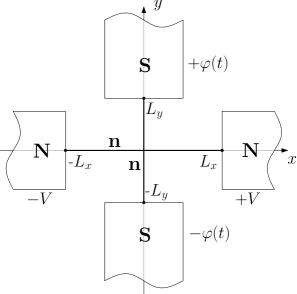
We consider an S/N structure shown in Fig. 1. It consists of a wire or film which connects two and reservoirs ( and stand for a normal metal, means a superconductor). The superconducting reservoirs may be connected by a superconducting contour. The transverse dimensions of the wire are supposed to be smaller than characteristic dimensions of the problem, but larger than the Fermi wave length and the mean free path (diffusive case). This implies that all quantities depend only on coordinates along the wire (the coordinate in the horizontal direction and the coordinate in the vertical direction). The dc voltage is applied between the normal reservoirs, and the phase difference exists between the superconducting reservoirs. The phase is assumed to be time-dependent
| (1) |
and related to the magnetic flux inside the superconducting contour:
with , where is
an applied magnetic field and is the area of the superconducting
contour; that is, the magnetic field contains not only a constant component,
but also an oscillating one.
For simplicity, we assume the structure to be symmetric both in the horizontal and vertical directions. This implies, in particular, that the interface resistances at are equal to each other (correspondingly, ). Our aim is to calculate the differential dc conductance between the reservoirs
| (2) |
as a function of the amplitude of the ac signal and the
frequency .
The calculations will be carried out on the basis of the well developed quasiclassical Green’s functions technique (see the reviewsLarkin and Ovchinnikov (1969); Rammer and Smith (1986); Belzig et al. (1999); Kopnin (2001)) which successfully was applied to the study of structures (see for exampleVolkov et al. (1993); Lambert and Raimondi (1998); Nazarov (1999); Belzig et al. (1999); Kogan et al. (2002); Volkov and Pavlovskii (1996); Golubev and Zaikin (2009); Golubov et al. (1997); Artemenko and Volkov (1979)). In this technique, all types of Green’s functions (the ”normal” and Gor’kov’s functions as well as the retarded, advanced and Keldysh functions) are matrix elements of a matrix
| (3) |
where are matrices of the retarded (advanced)
Green’s functions, and is a matrix of the Keldysh
functions. The first matrices describe thermodynamical properties of the
system (the density of states, supercurrent etc), whereas the matrix
is used to describe dissipative transport and nonequilibrium
properties.
The matrix satisfies the normalization conditionLarkin and Ovchinnikov (1975)
| (4) |
where ”” denotes the integral product
and ”” is the conventional matrix product. The Fourier transform performed
as
yields
where now .
The matrix of Keldysh functions can be expressed in terms of the matrices and a matrix of distribution functions :
| (5) |
where the matrix can be assumed to be diagonal Belzig et al. (1999):
| (6) |
Here is the identity matrix and the third Pauli matrix. The function describes
the charge imbalance (premultiplied with the DOS and integrated over all energies
it gives the local voltage), while characterizes the energy distribution of quasiparticles.
Due to the general relationRammer and Smith (1986)
| (7) |
one can immediately calculate after finding the matrix . That means that
knowing the matrices and we can determine all entries of .
The Green’s functions in and reservoirs are assumed to have an equilibrium form corresponding to the voltages and phases . For example, the retarded (advanced) Green’s functions in the upper reservoir are
| (8) |
where is a unitary transformation matrix and the Fourier transform of equals
| (9) |
with , i.e. the matrix
describes the BCS superconductor in the absence of phase.
The retarded (advanced) Green’s functions in the lower reservoir are
determined in the same way with the replacement .
The matrix in the right (left) reservoirs is equal to
with , i.e. .
In the reservoirs the matrix can be represented through the equilibrium distribution via Eq. (8)
| (10) |
The phase in the upper reservoir is given by Eq. (1), and for in the right reservoir, we have: . Therefore in the normal reservoir (at the right) the matrix distribution function has diagonal elements , and can be written as
| (11) |
Thus, all Green’s functions in the reservoirs are defined above.
Our task is to find the matrix in the wire. In the considered diffusive limit it obeys the equationLarkin and Ovchinnikov (1975)
| (12) |
where is a diagonal matrix with equal elements , is a local electrical potential in the wire. We dropped the inelastic collision term supposing that , where is the diffusion coefficient, and is an inelastic scattering time. This equation is complemented by the boundary conditionKupriyanov and Lukichev (1988)
| (13) |
where are the and interface resistances per unit area and is the conductivity of the wire. Here we introduced the commutator . The current in the wire is determined by the formula
| (14) |
The matrix element is the
Keldysh component that equals .
Even in a time-independent case, an analytical solution of the problem can by found only under certain assumptionsLambert and Raimondi (1998); Nazarov (1999); Belzig et al. (1999); Volkov and Pavlovskii (1996); Kogan et al. (2002); Volkov et al. (1993); Golubev and Zaikin (2009); Golubov et al. (1997). In the considered case of a time-dependent phase difference, the problem becomes even more complicated. In order to solve the problem analytically, we consider two limiting cases: a) weak proximity effect and slow phase variation in time; b) strong proximity effect in a short wire and arbitrary frequency of the phase oscillations.
III Weak Proximity Effect; Slow Phase Variation
In this section we will assume that the proximity effect is weak and the phase difference is almost constant in time. The latter assumption means that the frequency of phase variation satisfies the condition . The weakness of the PE means that the anomalous (Gor’kov’s) part of the retarded and advanced Green’s functions in the wire can be assumed to be small
| (15) |
The matrix contains only off-diagonal elements. The diagonal part obtained from the normalization is
| (16) |
Now we can linearize Eq. (12) for the component , that is, for the retarded (advanced) Green’s functions. Then we obtain a simple linear equation
| (17) |
where . The boundary conditions (13) for the matrices acquire the form
| (18) | |||
| (19) | |||
| (20) | |||
| (21) |
As follows from Eq. (8) the functions , are
| (22) | |||
| (23) |
We took into account that is almost constant in time.
One can show that the solution for in the horizontal part of the wire is
| (24) | |||
| (25) |
where is the sign function. Dropping the index of the quantities the integration constants and can be written as
| (26a) | |||
| (26b) | |||
where ,
, .
Knowing the function , one can find the correction to the conductance of the wire due to the PE. In order to obtain the current, we take the component (the Keldysh component) of Eq. (12), multiply this component by and take the trace. In the Fourier representation we get (compare with Eq. (2) of Ref. Kogan et al. (2002))
| (27) |
where the function determines the correction to the conductivity caused by the PE and is an integration constant that is related to the current:
| (28) |
It is determined from the boundary condition that can be obtained from Eq. (13)
| (29) |
where is the density of states in the wire near the interface. Finding and from Eq. (29), we obtain for the current density (compare with Eq. (13) of Ref. Volkov et al. (1993))
| (30) |
Here is defined according to Eq. (11), is the
resistance of the wire of the length in the normal state,
and .
The first term in the denominator is the interface resistance and the second term is the
resistance of the section of the wire modified by the PE.
The expressions for the DOS and the function
are given in appendix.
For the differential conductance at zero temperature we obtain
| (31) |
In Fig. 2 we show the dependence of the interface resistance variation and the resistance variation of the wire on the bias voltage for a fixed phase difference.
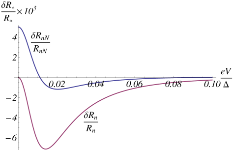
It can be seen that the is either positive or negative depending on ,
while is always negative, i.e. the PE leads to voltage dependent changes of the
interface resistance (caused by the changes of the DOS in the wire) and to a
decrease of the resistance of the wire.
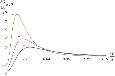
The conductance variation
, is shown in Fig. 3 for various values
of , where is the conductance
of the -wire in the normal state. These results have been obtained
earlierVolkov et al. (1993); Nazarov and Stoof (1996); Volkov and Pavlovskii (1996); Golubov et al. (1997).
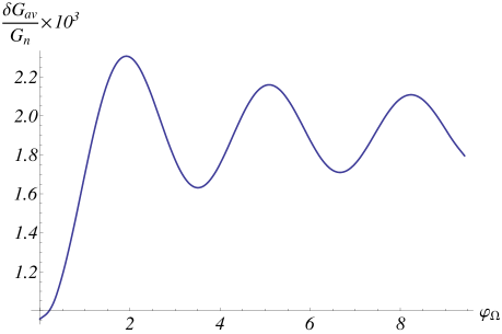
We are interested in the dc conductance variation averaged in time: . First, from Eqs. (25-26) we can extract the dependence of the function on the phase : . Hence we obtain where . At the same time, with . These observations lead to the relation
| (32) |
which by averaging over time yields
| (33) |
where is the Bessel function of the first kind and zeroth order. This oscillatory
behavior of the time-averaged (dc) conductance variation as a function of the
ac amplitude can be seen in Fig. 4.
Thus, the calculations carried out in this section under assumption of adiabatic phase variations allow us to obtain the dependence of the conductance change on the amplitude , but provide no information about the frequency dependence of . This dependence will be found in the next section.
IV Strong PE; Short Normal Wire
In this section we analyze the limiting case of a short wire when the Thouless energy is much larger than characteristic energies: . In this case all the functions in Eq. (12) are almost constant in space and we can integrate this equation from to over and coordinates. The term (in the Fourier representation ) is considered as a constant and the term with the voltage is omitted because we neglect the voltage drop over the wire; the voltage drops across the interfaces and is set to be zero in the wire. Performing this integration and summing up the results, we obtain
| (34) |
where , , and . Integration around the point yields the conservation of the ”currents” (using terminology of the circuit theoryNazarov (1999))
| (35) |
Combining Eqs. (34-35) and the boundary conditions (13), we arrive at the equation
| (36) |
Here is a characteristic energy
related to the interface transparencies, . The energy
determines the damping in the spectrum of the wire and
the energy is related to a subgap induced in the wire
due to the PE. The matrices are equal to:
.
In the limit of the short wire considered in this section, we need to find only the retarded (advanced) Green’s functions. Indeed, let us rewrite the expression for the current (14) using the boundary condition (13) at the right interface and concentrating on the dc component of the current:
| (37) |
where and . The distribution function in the reservoir is defined in Eq. (11). The integral over energies from the second and third term is zero because it is proportional to the voltage in the wire which is set to be zero. Therefore the current can be written as
| (38) |
where . This
formula has an obvious physical meaning - the current through the
interface is determined by the product of the DOS in the wire and
reservoir () and the distribution function in the reservoir
(the distribution function in the wire is zero).
Using Eqs. (2), (11), (38) we arrive at the following expression for the differential conductance:
| (39) |
In order to find the matrix , we can write the (11) component of Eq. (36) in the form
| (40) |
where , .
According to Eqs. (1), (8) the matrix is a function of
two times, , that is, in the Fourier representation it is function
of two energies: . Therefore, to find the matrix in a
general case is a formidable task.
However, we can assume that the amplitude of the ac component of the phase is small and obtain the solution making an expansion in powers of :
| (41) |
Here and later all matrix Green’s functions written without arguments are functions of two energies
. Those of them which are diagonal in energy may be also (explicitly) written with
a single energy argument, e.g. .
Similar to Eq. (41) we represent the matrix (up to the second order in ) as and find from Eq. (8) for the stationary part and the corrections (first order in ) and (second order in ):
| (42) |
| (43) |
| (44) |
where we used the notation , and defined the functions
| (45) |
Using the expressions for and given above we can calculate
the corrections to up to the second order in and the corresponding modification
of the DOS in the wire.
In the zeroth-order approximation, i.e. for we obtain from Eq. (40) where the matrix obeys the equation
| (46) |
containing , , , . The solution of this equation is Volkov et al. (1993)
| (47) |
where .
The quantity determines a subgap induced in the wire due
to the PE. Indeed, consider the most interesting case of small energies assuming that
; then, ,
and .
This means that the spectrum of the wire has the same form as in the BCS superconductor
with a damping and a subgap ,
which depends on the interface transparency and phase difference.
Note that the formula for the subgap induced in the N metal due to
the PE in a tunnel SIN junction was obtained by McMillanMcMillan (1968).
The obtained results for the functions and can be easily generalized for the case of asymmetric interfaces with different interface resistances (correspondingly, ). In the limit , we obtain for the subgap
| (48) |
This formula shows that that the subgap as a function of the phase
difference varies from
for to
for .
We proceed finding the corrections of the first () and second () order in for in a way similar to the one used inArtemenko and Volkov (1979); Zaitsev et al. (1999). The correction of the first order (for brevity, we drop the index ) obeys the equation
| (49) |
which contains all terms of the first order in from Eq. (40).
Note, that we are making use of the relation
evident from Eqs. (40), (46-47).
In order to solve Eq. (49), it is useful to employ the normalization condition (4) for which for the first-order term of yields
| (50) |
| (51) |
We determine the correction in the same manner. Reading off the second-order terms in Eq. (40) gives
| (52) |
The second-order part of the normalization condition is
| (53) |
Thus, we obtain the second-order correction
| (54) |
In order to calculate the correction to the dc conductance caused by
the ac radiation, , we need to find
and and take their parts proportional to
. By inspection of Eqs. (43), (51) one
recognizes that the first-order correction contains only terms proportional to
and therefore only contributes to the ac current.
This is the fundamental reason why the second-order analysis is needed to determine
the variation of the dc conductance.
As a result we just have to find the multiple of contained in
which we denote as , that is
.
We represent the function as a sum
| (55) |
where the function originates from the first term in Eq. (54) and the function from the second and third terms. If we consider the case when the subgap is much less than , i.e.
| (56) |
then, at low energies , the function is almost independent of , whereas the function depends strongly on at . Assuming the validity of Eq. (56) we obtain
| (57) |
| (58) |
where the functions , , are defined in
Eq. (47). The sum sign index ”” in Eq. (58)
means that the given expression is added to the same one with the negative frequency .
Using the function we can calculate a correction to the DOS due to the PE and with the aid of Eq. (39) find the correction to the differential dc conductance. As follows from Eq. (39), at zero temperature the normalized differential dc conductance is equal to
| (59) |
with the definitions and .
Using the obtained formula for and
we can calculate the conductance and its correction
due to microwave radiation for different values of parameters
(damping , phase difference , etc.). The dependence of the conductance in the absence
of radiation versus the applied voltage is presented in
Fig. 5. We see that this dependence follows the energy
dependence of a SIN junction. In our case the wire with an induced subgap
plays a role of ”S” with a damping in the ”superconductor”.
Since the value of the induced subgap, ,
depends on the phase difference , the position of the peak in
the dependence is shifted downwards with increasing .
Note that in an asymmetrical system () the
lowest value of the subgap is not zero (cf. Eq. (48)).

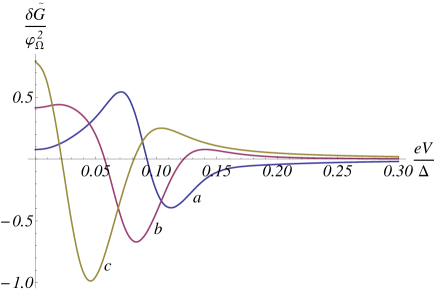
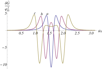
In Fig. 6 we show the bias voltage dependence of the conductance
correction due to ac radiation (coefficient in front of )
for different values of .
The magnitude and the position of the arising peaks depend strongly on the values of the parameters,
e.g. .
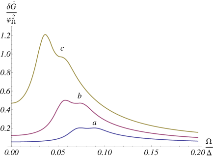
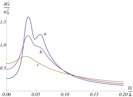
By varying the stationary phase difference or the damping
one can change the frequency dependence of the correction considerably.
This is shown in Fig. 7 and Fig. 8 respectively.
One can see that if , then the dependence
has a peak located at
and split into two subpeaks. The splitting becomes more and more distinct with increasing bias voltage V.
With decreasing and increasing , the form of this dependence changes
significantly. For example, the resonance curve becomes broader with increasing damping.
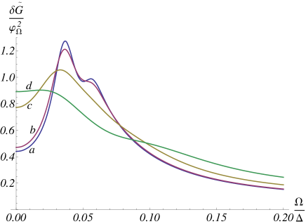
Increasing temperature leads to a similar effect as one can see in
Fig. 9.
In Fig. 10 we plot the normalized conductance correction as a function of for different values of the bias voltage . At large this dependence is close to sinusoidal, but at smaller voltages the form of the periodic function becomes more complicated.
V Conclusion
We have calculated the change of the conductance in an S/N
structure of the cross geometry under the influence of microwave radiation.
The calculations have been carried out on the basis of quasiclassical
Green’s functions in the diffusive limit. Two different limiting cases have
been considered: a) a weak proximity effect and low frequency of
radiation; b) a strong proximity effect and small amplitude of radiation.
In the case a), the conductance change consists of two parts. One
is related to a change of the interface resistance due to a
modification of the DOS of the wire. At small applied voltages
it is negative. Another part is caused by a modification of the conductance
of the wire due to the PE. This part is positive and consists of two
competing contributions. One contribution, which is negative, stems from the
a modification of the DOS of the wire. Another contribution is positive
and caused by a term, which is similar to the Maki-Thompson termVolkov and Pavlovskii (1996); Golubov et al. (1997). The conductance change oscillates and
decays with increasing amplitude of radiation.
In the case b) a short wire was considered so that the
resistance of the wire is negligible in comparison with the
resistance of the interface. The correction has
been found under assumption of a small amplitude of the radiation.
We found that at small applied voltages , the dependence
has a resonance
form. It has a maximum when the frequency is of the order of
where is a
subgap in the spectrum of the wire induced by the PE. With increasing ,
the peak in the dependence splits into two peaks and
overall form of this dependence becomes complicated.
We assumed that the interface resistance is larger
than the resistance of the wire, that is: .
This inequality can be written in the form , that is, the subgap energy in the
wire is much smaller than the Thouless energy . In the
opposite limit, , a gap of the order of
is induced in the wire. This limit can be studied numerically.
However, one can expect that in this limit the resonance should take place at
. Experiment performed in Ref.Checkley et al. (2010)
corresponds to this limit. The frequency corresponding to the Thouless
energy in experiment is equal to
,
whereas the resonance frequency is .
Note that we considered a simplified model. For example, we did not
account for the change of the distribution function in the
film (heating effects). One can give estimations when the ”heating” can be
neglected. The change of an ”effective” electron temperature
in the wire is approximately given by:
, where
is the electron-phonon inelastic scattering time,
is the ac electric field in the wire and
is the heat capacity of electron
gas with concentration . Taking into account that ,
we find that
,
where is the dimensionless coefficient of electron penetration through the SN interface,
which is assumed to be small, is the mean free path in the wire.
Therefore, the heating would be very small if the condition
is fulfilled.
The obtained results are useful for understanding the response of
the considered and analogous SN systems to microwave radiation which can be
used, for example, in Q-bits.
We would like to thank SFB 491 for financial support. One of us (VTP) was supported by the British EPSRC (Grant EP/F016891/1).
VI Appendix
Making use of the weak proximity effect approximation the function we rewrite in Eq. (30) as
| (60) |
Using Eq. (25) one can easily calculate
| (61) | |||
| (62) |
where and are the real and imaginary parts of respectively, i.e.
.
We use these expressions for calculating the function and conductance .
References
- Petrashov et al. (1992) V. T. Petrashov, V. N. Antonov, and M. Persson, Physica Scripta T42, 136 (1992), see also ”Low Dimensional Properties of Solids” (Proceedings of the Nobel Jubilee Symposium, Göteborg, Sweden, December 4-7,1991) ed. M. Jonson and T. Claeson, World Scientific Publishing,1992.
- Petrashov et al. (1993) V. T. Petrashov, V. N. Antonov, P. Delsing, and R. Claeson, Phys. Rev. Lett. 70, 347 (1993), ibid 74, 5268 (1995).
- Pothier et al. (1994) H. Pothier, S. Guéron, D. Esteve, and M. H. Devoret, Phys. Rev. Lett. 73, 2488 (1994).
- de Vegvar et al. (1994) P. G. N. de Vegvar, T. A. Fulton, W. H. Mallison, and R. E. Miller, Phys. Rev. Lett. 73, 1416 (1994).
- Dimoulas et al. (1995) A. Dimoulas, J. P. Heida, B. J. v. Wees, T. M. Klapwijk, W. v. d. Graaf, and G. Borghs, Phys. Rev. Lett. 74, 602 (1995).
- Eom et al. (1998) J. Eom, C.-J. Chien, and V. Chandrasekhar, Phys. Rev. Lett. 81, 437 (1998).
- Beenakker (1995) C. W. J. Beenakker, in Mesoscopic Quantum Physics (North-Holland, Amsterdam, 1995), ed. by E. Akkermans, G. Montambaux, J.-L. Pichard and J. Zinn-Justin.
- Lambert and Raimondi (1998) C. J. Lambert and R. Raimondi, J. Phys.: Condens. Matter 10, 901 (1998).
- Nazarov (1999) Y. V. Nazarov, Superlattices and Microstructures 25, 1221 (1999).
- Belzig et al. (1999) W. Belzig, F. K. Wilhelm, C. Bruder, G. Schön, and A. D. Zaikin, Superlattices and Microstructures 25, 1251 (1999).
- Volkov et al. (1993) A. Volkov, A. Zaitsev, and T. Klapwijk, Physica C: Superconductivity 210, 21 (1993).
- Hekking and Nazarov (1993) F. W. J. Hekking and Y. V. Nazarov, Phys. Rev. Lett. 71, 1625 (1993).
- Zaitsev (1994) A. Zaitsev, Physica B: Condensed Matter 203, 274 (1994).
- Nazarov and Stoof (1996) Y. V. Nazarov and T. H. Stoof, Phys. Rev. Lett. 76, 823 (1996).
- Artemenko et al. (1979) S. N. Artemenko, A. F. Volkov, and A. V. Zaitsev, Solid State Communications 30, 771 (1979).
- Volkov et al. (1996) A. Volkov, N. Allsopp, and C. J. Lambert, Journal of Physics: Condensed Matter 8, L45 (1996).
- Volkov (1995) A. F. Volkov, Phys. Rev. Lett. 74, 4730 (1995).
- Wilhelm et al. (1998) F. K. Wilhelm, G. Schön, and A. D. Zaikin, Phys. Rev. Lett. 81, 1682 (1998).
- Yip (1998) S.-K. Yip, Phys. Rev. B 58, 5803 (1998).
- Gubankov and Margolin (1979) V. N. Gubankov and N. M. Margolin, JETP Lett. 29, 673 (1979).
- Charlat et al. (1996) P. Charlat, H. Courtois, P. Gandit, D. Mailly, A. F. Volkov, and B. Pannetier, Phys. Rev. Lett. 77, 4950 (1996).
- Petrashov et al. (1996) V. Petrashov, R. Shaikhaidarov, and I. Sosnin, JETP Letters 64, 839 (1996).
- Baselmans et al. (1999) J. J. A. Baselmans, A. F. Morpurgo, B. J. van Wees, and T. M. Klapwijk, Nature 397, 43 (1999).
- Shaikhaidarov et al. (2000) R. Shaikhaidarov, A. F. Volkov, H. Takayanagi, V. T. Petrashov, and P. Delsing, Phys. Rev. B 62, R14649 (2000).
- Golubov et al. (2004) A. A. Golubov, M. Y. Kupriyanov, and E. Il’ichev, Rev. Mod. Phys. 76, 411 (2004).
- Buzdin (2005) A. I. Buzdin, Rev. Mod. Phys. 77, 935 (2005).
- Bergeret et al. (2005) F. S. Bergeret, A. F. Volkov, and K. B. Efetov, Rev. Mod. Phys. 77, 1321 (2005).
- Tsuei and Kirtley (2000) C. C. Tsuei and J. R. Kirtley, Rev. Mod. Phys. 72, 969 (2000).
- Van Harlingen (1995) D. J. Van Harlingen, Rev. Mod. Phys. 67, 515 (1995).
- Bezryadin et al. (2000) A. Bezryadin, C. N. Lau, and M. Tinkham, Nature 404, 971 (2000).
- Zgirski et al. (2005) M. Zgirski, K.-P. Riikonen, V. Touboltsev, and K. Arutyunov, Nano Letters 5, 1029 (2005).
- Tian et al. (2005) M. Tian, N. Kumar, S. Xu, J. Wang, J. S. Kurtz, and M. H. W. Chan, Phys. Rev. Lett. 95, 076802 (2005).
- Arutyunov et al. (2008) K. Arutyunov, D. Golubev, and A. Zaikin, Physics Reports 464, 1 (2008).
- Petrashov et al. (2005) V. T. Petrashov, K. G. Chua, K. M. Marshall, R. S. Shaikhaidarov, and J. T. Nicholls, Phys. Rev. Lett. 95, 147001 (2005).
- Chiodi et al. (2009) F. Chiodi, M. Aprili, and B. Reulet (2009), arXiv:0908.1070.
- Checkley et al. (2010) C. Checkley, A. Iagallo, R. Shaikhaidarov, J. T. Nicholls, and V. T. Petrashov (2010), arXiv:1003.2176.
- Golubev and Zaikin (2009) D. Golubev and A. Zaikin, Europhys. Lett. 86, 37009 (2009).
- Virtanen et al. (2010) P. Virtanen, T. T. Heikkilä, F. S. Bergeret, and J. C. Cuevas (2010), arXiv:1001.5149.
- Giazotto et al. (2006) F. Giazotto, T. T. Heikkila, A. Luukanen, A. M. Savin, and J. P. Pekola, Rev. Mod. Phys. 78, 217 (2006).
- Usadel (1970) K. D. Usadel, Phys. Rev. Lett. 25, 507 (1970).
- Larkin and Ovchinnikov (1969) A. I. Larkin and Y. N. Ovchinnikov, Sov. Phys. JETP 28, 1200 (1969), [Zh. Eksp. Teor. Fiz. 55, 2262 (1968)].
- Rammer and Smith (1986) J. Rammer and H. Smith, Rev. Mod. Phys. 58, 323 (1986).
- Kopnin (2001) N. B. Kopnin, Theory of Nonequilibrium Superconductivity (Clarendon Press, Oxford, 2001).
- Kogan et al. (2002) V. R. Kogan, V. V. Pavlovskii, and A. F. Volkov, Europhys. Lett. 59, 875 (2002).
- Volkov and Pavlovskii (1996) A. F. Volkov and V. V. Pavlovskii, in Proceedings of the 21st Rencontres de Moriond (Les Arcs, France, 1996), p. 267.
- Golubov et al. (1997) A. A. Golubov, F. K. Wilhelm, and A. D. Zaikin, Phys. Rev. B 55, 1123 (1997).
- Artemenko and Volkov (1979) S. N. Artemenko and A. F. Volkov, Soviet Physics Uspekhi 22, 295 (1979).
- Larkin and Ovchinnikov (1975) A. I. Larkin and Y. N. Ovchinnikov, Sov. Phys. JETP 41, 960 (1975), [Zh. Eksp. Teor. Fiz. 68, 1915 (1975)].
- Kupriyanov and Lukichev (1988) M. Y. Kupriyanov and V. F. Lukichev, Sov. Phys. JETP 67, 1163 (1988), [Zh. Eksp. Teor. Fiz. 94, 139 (1988)].
- McMillan (1968) W. L. McMillan, Phys. Rev. 175, 537 (1968).
- Zaitsev et al. (1999) A. V. Zaitsev, A. F. Volkov, S. W. D. Bailey, and C. J. Lambert, Phys. Rev. B 60, 3559 (1999).