Semi-Empirical Model for Nano-Scale Device Simulations
Abstract
We present a new semi-empirical model for calculating electron transport in atomic-scale devices. The model is an extension of the Extended Hückel method with a self-consistent Hartree potential. This potential models the effect of an external bias and corresponding charge re-arrangements in the device. It is also possible to include the effect of external gate potentials and continuum dielectric regions in the device. The model is used to study the electron transport through an organic molecule between gold surfaces, and it is demonstrated that the results are in closer agreement with experiments than ab initio approaches provide. In another example, we study the transition from tunneling to thermionic emission in a transistor structure based on graphene nanoribbons.
pacs:
73.40.-c, 73.63.-b, 72.10.-d, 72.80.VpI Introduction
As the minimum feature sizes of electronic devices are approaching the atomic scale, it becomes increasingly important to include the effects of single atoms in device simulations. In recent years, there have been several developments of atomic-scale electron transport simulation models based on the Non-Equilibrium Green’s Function (NEGF) formalismHaug and Jauho (1996). The approaches can roughly be divided into two catagories: ab initio approaches, where the electronic structure of the system is calculated from first principles, typically with Density Functional Theory (DFT)Lang (1995); Xue (2002); Brandbyge et al. (2002); Taylor et al. (2001), and semi-empirical approaches, where the electronic structure is calculated using a model with adjustable parameters fitted to experiments or first-principles calculations. Examples of semi-empirical transport models are methods based on Slater-Koster tight-binding parametersDi Carlo (2002); Pecchia and Di Carlo (2004) and Extended Hückel parametersMagoga and Joachim (1997); Corbel et al. (1999); Cerdá and Soria (2000); Emberly and Kirczenow (2001); Zahid et al. (2005); Kienle et al. (2006, 2006).
The ab initio models have the advantage of predictive power, and can often give reasonable results for systems where there is no prior experimental data. However, the use of the Kohn-Sham one-particle states as quasiparticles is questionable, and it is well known that for many systems the energies of the unoccupied levels are rather poorly described within DFT. Furthermore, solving the Kohn-Sham equations can be computationally demanding, and solving for device structures with thousands of atoms is only feasible on large parallel computers.
The semi-empirical models have less predictive power, but when used within their application domain they can give very accurate results. The models may also be fitted to experimental data, and can thus in some cases give more accurate results than DFT-based methods. However, the main advantage of the semi-empirical methods are their lower computational cost.
In this paper we will present the formalism behind a new semi-empirical transport model based on the Extended Hückel (EH) method. The model can be viewed as an extension to the work by Zahid et al.Zahid et al. (2005), with the main difference being the treatment of the electrostatic interactions. Zahid et al. only describe part of the electrostatic interactions in the device; most importantly, they use the Fermi level of the electrodes as a fitting parameter and do not account for the charge transfer from the electrodes to the device. In the current work, the Fermi level of the electrodes is determined self-consistently by using the methodology introduced by Brandbyge et al.Brandbyge et al. (2002) In this way, we include the charge transfer from the electrodes to the device region and describe all electrostatic interactions self-consistently. This is accomplished by defining a real-space electron density and numerically solving for the Hartree potential on a real-space grid. Through a multi-grid Poisson solver, we include the self-consistent field from an applied bias, and allow for including continuum dielectric regions and electrostatic gates within the scattering region.
The organization of the paper is the following: In section II we introduce the self-consistent Extended Hückel (EH-SCF) model, and in section III we present the formalism for modelling nano-scale devices. In section IV we apply the model to a molecular device, and in section V we consider a graphene nano-transistor where an electrostatic gate is controlling the electron transport in the device. Finally, in section VI, we conclude the paper.
II The Self-Consistent Extended-Hückel method
In this section we describe the EH-SCF framework. In Extended Hückel theory, the electronic structure of the system is expanded in a basis set of local atomic orbitals (LCAOs)
| (1) |
where is a spherical harmonic and is a superposition of Slater orbitals
| (2) |
The LCAOs are described by the adjustable parameters , , , and , and these parameters must be defined for the valence orbitals of each element.
The central object in EH theory is the overlap matrix,
| (3) |
where is a composite index for and is the position of the center of orbital .
From the overlap matrix, the one-electron Hamiltonian is defined by
| (4) |
where is an orbital energy, and is an adjustable parameter (often chosen to be 1.75). is the Hartree potential corresponding to the induced electron density on the atoms, i.e. the change in electron density compared to a superposition of neutral atomic-like densities. This term must be determined self-consistently, and is not included in standard EH modelsWhangbo and Hoffmann (1978). In the following section we describe how this term is calculated.
II.1 Solving the Poisson Equation to Obtain the Hartree Potential
To calculate the induced Hartree potential we need to determine the spatial distribution of the electron density. To this end, we introduce the Mulliken population of atom number
| (5) |
where is the density matrix. The total number of electrons can now be written as a sum of atomic contributions, .
We will represent the spatial distribution of each atomic contribution by a Gaussian function, and use the following approximation for the spatial distribution of the induced electron density:
| (6) |
where the weight of each Gaussian is the excess charge of atom as obtained from the Mulliken population and the ion valence charge . Subsequently, the Hartree potential is calculated from the Poisson equation
| (7) |
which is solved with the appropriate boundary conditions on the leads and gate electrodes imposed by the applied voltages. Here, is the spatially dependent dielectric constant of the device constituents, and allows for the inclusion of dielectric screening regions.
To see the significance of the width of the Gaussian orbital, let us calculate the electrostatic potential from a single Gaussian electron density at position . The result is
| (8) |
and from this equation we see that the on-site value of the Hartree potential is , where the parameter
| (9) |
is the on-site Hartree shift. The parameter is a well-known quantity in CNDO theoryPople and Segal (1966); Murell and Harget (1972), and values of are listed for many elements in the periodic table. Thus, we fix the value of using CNDO theory, and then use Eq. (9) to calculate the value of for each element.
III EH-SCF Method for a Nano-Scale Device
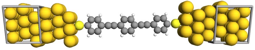
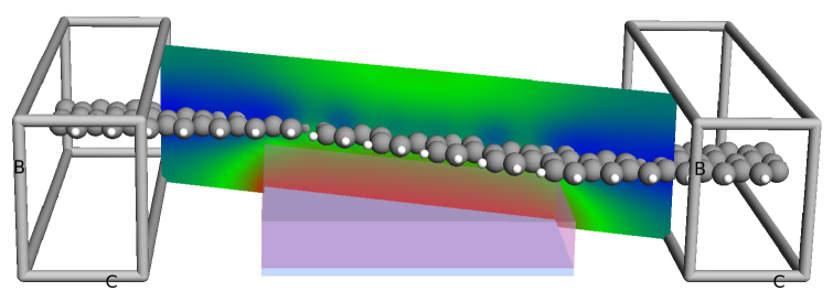
Fig. 1 illustrates the setup of a molecular device system. The system consists of three regions: the central region, and the left and right electrode regions. The central region includes the active parts of the device and sufficient parts of the contacts, such that the properties of the electrode regions can be described as bulk materials. For metallic contacts, this will typically be achieved by extending the central region 5–10 Å into the contacts.
The calculation of the electron transport properties of the system is divided into two parts. The first part is a self-consistent calculation for the electrodes, with periodic boundary conditions in the transport direction. In the directions perpendicular to the transport direction, we apply the same boundary conditions for the two electrodes and the central region, and these boundary conditions are described below.
In the second part of the calculation, the electrodes define the boundary conditions for a self-consistent open boundary calculation of the properties of the central region. The main steps in the open boundary calculation is the determination of the density matrix, the evaluation of the real-space density, and, finally, the calculation of the Hartree potential. These steps will be described in more detail in the following section.
III.1 Calculating the Self-Consistent Density Matrix of the Central Region
In this section we will describe the calculation of the density matrix of the central region. We assume that the self-consistent properties of the left and right electrodes have already been obtained, and thus we also know their respective Fermi levels, and . We allow for an external bias to be applied between the two electrodes, and define the left and right chemical potentials and . The applied bias thus shifts all energies in the left electrode, and a positive bias gives rise to an electrical current from left to right.
The density matrix for this non-equilibrium system, with two different chemical potentials, is found by filling up the left and right originating states according to their respective chemical potentialsTodorov et al. (2000); Brandbyge et al. (2002),
| (10) |
where () is the contribution to the spectral density of states from scattering states originating in the left (right) reservoir.
The calculation of the spectral densities is performed using NEGF theory, and we write the partial spectral densities as
| (11) |
where is the retarded Green’s function of the central region, and the broadening function is given by the self energies and , which arise due to the coupling of the central region with the semi-infinite left and right electrodes, respectively.
Further details of the NEGF formalism can be found in Refs. Haug and Jauho, 1996,Brandbyge et al., 2002. Here we just note that to improve the numerical efficiency, the integral in Eq. (10) is divided into an equilibrium and non-equilibrium part. The equilibrium part is calculated on a complex contour far from the real-axis poles of the Green’s function, and only the non-equilibrium part is performed along the real axis. The equilibrium and non-equilibrium parts are then joined using the double-contour technique introduced by Brandbyge et al.Brandbyge et al. (2002)
From the density matrix we may now evaluate the real-space density in the central region using Eq. (6). It is important to note that near the left and right faces of the central region there will be contributions from the electrode regions, and this “spill in” must be properly accounted for.
Once the real-space density is known, the Hartree potential is calculated by solving the Poisson equation in Eq. (7) using a real-space multi-grid method. On the left and right faces of the central region the Hartree potential is fixed by the electrode Hartree potentials, appropriately shifted according to the applied bias. In the directions perpendicular to the transport directions, we apply the appropriate boundary conditions, fixed or periodic, as demanded by e.g. the presence of gate electrodes.
III.2 Transmission and Current
Once the self-consistent one-electron Hamiltonian has been obtained, we can finally evaluate the transmission coefficients Haug and Jauho (1996); Datta (1997)
| (12) |
and the current
| (13) |
In the following sections, we apply this formalism to the calculation of the electrical properties of a molecule between gold electrodes, as well as a graphene nano-transistor.
IV Tour Wire between Gold Electrodes
In this section we will investigate the electrical properties of a phenylene ethynylene oligomer, also popularly called a Tour wire. We will compare the electrical properties of the molecule when it is symmetrically and asymmetrically coupled with two Au(111) surfaces. In the symmetric system, as illustrated in Fig. 1, the molecule is connected with both gold surfaces through thiol bonds, whereas the asymmetric system only has a thiol bond to one of them.
The system has previously been investigated experimentally by Kushmerick et al.Kushmerick et al. (2002) and theoretically by Taylor et al.Taylor et al. (2002), and it has been found that the asymmetrically coupled system shows strongly asymmetric I–V characteristicsKushmerick et al. (2002).
The calculations by Taylor et al. were based on DFT-LDA, and the asymmetric behaviour could be related to the voltage drop in the system. This system is therefore an excellent testing ground for our semi-empirical model, since a correct description of the electrical properties requires not only a good model for the zero-bias electronic structure, but also a good description of the bias-induced effects.
IV.1 Transmission Spectrum of the Symmetric Tour Wire Junction
To setup the symmetric system we first relaxed the isolated Tour wire using DFT-LDAATK . During the relaxation, passivating hydrogen atoms were kept on the sulfur atoms. Afterwards, these hydrogen atoms were removed and the two sulfur atoms placed at the FCC sites of two Au(111)-(3x3) surfaces. The height of the S atom above the surface was 1.9 Å (corresponding to an Au–S distance of 2.53 Å).
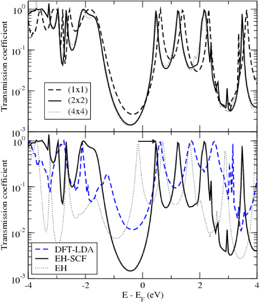
We next set up the EH model with Hoffmann parametersWhangbo and Hoffmann (1978); Ammeter et al. (1978) and perform a self-consistent calculation to obtain transmission spectra for different k-point sampling grids. The results are shown in the upper plot of Fig. 2. In each case, the same k-point grid was used for both the self-consistent and transmission calculation, and we see from the figure that using (1x1) k-point is insufficient while (2x2) and (4x4) k-points give almost identical results. Thus, we will use a (2x2) k-point sampling grid for the remainder of this study.
In the lower plot of Fig. 2 we compare the transmission spectra calculated with DFT-LDA, EH-SCF, and EH without the Hartree term of Eq. (4). For the DFT-LDA model we use similar parameters as Taylor et al.Taylor et al. (2002), except for the k-point sampling which is (2x2) in the current study. The calculations in Ref. Taylor et al., 2002 were performed with a (1x1) k-point sampling, which is insufficientThygesen and Jacobsen (2005), and thus the DFT-LDA results in this study will differ from those by Taylor et al.
For the EH calculation we see a peak in the transmission spectrum just around the Fermi level of the gold electrodes. This peak arises from transmission through the LUMO orbital of the Tour wire.
In the self-consistent EH calculation there will be a charge transfer from the gold surface to the LUMO orbital, and we see that this gives rise to a shift of the orbital by 1 eV, illustrated by the arrow in Fig. 2.
For the DFT-LDA calculation we see that the LUMO peak is shifted further away from the gold Fermi level, and the HOMO and LUMO peaks of the transmission spectrum are placed almost symmetrically around the gold Fermi level. We also note that the transmission coefficient at the Fermi level, corresponding to the zero-bias conductance, is almost one order of magnitude higher within the DFT-LDA model. We will discuss this further below.
We also note that Taylor et al. find a LUMO level even further away from the gold Fermi level; this is related to the insufficient k-point sampling.
IV.2 I–V Characteristics of the Symmetric and Asymmetric Tour Wire Systems
We will now study both the symmetric and asymmetric Tour wire system and compare their respective I–V characteristics. The geometry of the asymmetric system is illustrated in Fig. 3. The geometry is similar to that of Fig. 1, except for the right-most sulfur atom which has been replaced by a hydrogen atom with a C–H bond length of 1.1 Å. The distance between the hydrogen atom and the right gold surface is 1.5 Å.

We perform self-consistent calculations for both the symmetric and asymmetric systems with the EH-SCF and DFT-LDA methods, and vary the bias from –1 to +1 V in steps of 0.1 V. The results are shown in Fig. 4. For the symmetric device we obtain rather similar, symmetric I–V characteristics for both the EH-SCF and DFT-LDA methods. The main difference is that the zero-bias conductance is significantly higher with DFT-LDA, reflecting the higher transmission coefficient at the Fermi level, as shown in Fig. 2.
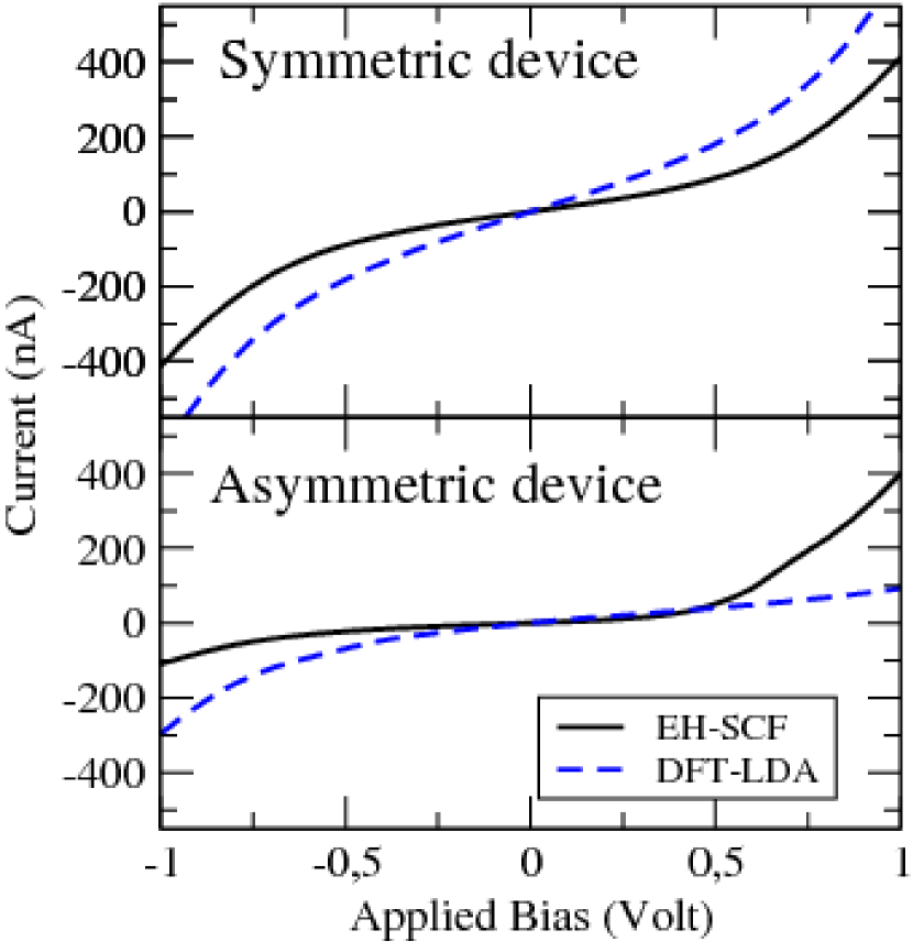
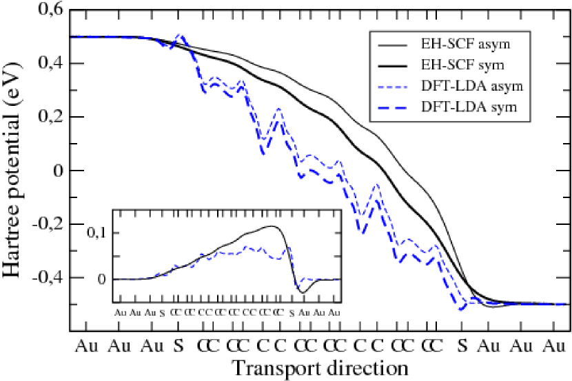
For the asymmetric device we see that both the DFT-LDA and EH-SCF models give rise to rectification – however, in opposite directions. Taylor et al.Taylor et al. (2002) demonstrated that the rectification was related to the voltage drop in the system, and we therefore in Fig. 5 compare the voltage drops obtained with the two methods. The EH-SCF voltage drop is smooth, since the charge density is composed of a superposition of single rather broad Gaussians on each atom. The DFT-LDA model shows atomic-scale details, however, as illustrated by the inset, the relative change in the voltage drop between the asymmetric and symmetric system is quite similar for the EH-SCF and DFT-LDA methods. Both methods reveal that in the asymmetric system there is an additional voltage drop at the contact with the weak bond. This is also one of the main results of Taylor et al.Taylor et al. (2002).
The additional voltage drop at the weak contact means that the molecular levels of the Tour wire mainly follow the electrochemical potential of the right electrodeTaylor et al. (2002). Since the voltage drop is similar for the DFT-LDA and EH-SCF models, the difference in the I–V characteristics must be related to the different electronic structure at zero bias in the two models. Within the DFT-LDA model, the transport at the Fermi level is dominated by the HOMO. At negative bias, the left electrode has a higher electrochemical potential, and electrons from the occupied HOMO level can propagate to empty states in the left electrode. Thus, for the DFT-LDA model, the current is highest for a negative bias at the left electrode. For the EH-SCF model, on the other hand, the transport at the Fermi level is dominated by the LUMO, and the current in this case is highest for a positive bias at the left electrode.
Comparing with the experimental results of Kushmeric et al.Kushmerick et al. (2002), we find that the EH-SCF rectification direction agrees with the experimental rectification direction, while the DFT-LDA model predicts rectification in the opposite direction. We note that the rectification direction obtained with our DFT-LDA model is similar to the results of Taylor et al.Taylor et al. (2002).
Thus, for this system it seems that the EH-SCF model is in better agreement with the experimental results, compared to the DFT-LDA model. The example shows that the EH-SCF model gives a very good description of both the electronic structure and the voltage drop in the system. The comparisons between the two methods also illustrates how small variations in the positions of the HOMO and LUMO levels may change the electrical properties of the Tour wire device.
V Z-Shaped Graphene Nano-Transistor
In this section we will compare the electrical properties of a short (34 Å) and long (86 Å) graphene nano-transistor. The system consists of two electrodes consisting of metallic, zigzag-edge graphene nanoribbons connected through a semiconducting armchair-edge central ribbon. The system is placed 1.4 Å above a dielectric material with dielectric constant , corresponding to SiO2. The dielectric is 3 Å thick, and below the dielectric there is an electrostatic gate. The geometry of the short system is illustrated in Fig. 6. A similar system was investigated by Yan et al.Yan et al. (2007) using DFT-LDA.
For the calculation we use EH parameters from Ref. Kienle et al., 2006 which were derived by fitting to a reference band structure of a graphene sheet calculated with DFT-LDA. With these parameters, we find a band gap of the central ribbon of 2.2 eV, in agreement with DFT-LDA calculations, which illustrates the transferability of the EH parameters from 2D graphene to a 1D graphene nanoribbon.
V.1 Transmission Spectrum
Fig. 7 shows the transmission spectrum for both the long and the short system when there is no applied bias and zero gate potential. The shape of the transmission spectrum is directly related to the electronic structure of the central semiconducting ribbon.

The transmission is strongly reduced in the energy region from –0.7 to 1.5 eV, corresponding to the band gap of the central armchair ribbon. Since there are no energy levels in this interval, the electrons must tunnel in order to propagate across the junction. For the longer device the electrons must tunnel a longer distance, and thus the transmission is more strongly reduced.
Outside the band gap, the transmission is close to 1 and shows a number of oscillations. Since the central ribbon has a finite length, it resembles a molecule with a number of discrete energy levels. The levels give rise to peaks in the transmission spectrum, and since the longer system has more energy levels, the peaks are more closely spaced there.
In the following section we will see how this difference in the transmission spectrum gives rise to qualitatively different transport mechanisms in the two devices.
V.2 Transistor Characteristics
We now calculate the current for an applied source–drain voltage of 0.2 V as a function of the applied gate potential. Fig. 8 shows the current for the long and short devices, respectively, for gate potentials in the range –1 to 1 V, for different electrode temperatures. We see that for the short device there is only a small effect of the gate potential and electron temperature, while for the long device the conductance falls off exponentially, reaching a minimum in the range 0 to 0.5 V. Moreover, the current is strongly temperature-dependent.
The lack of temperature-dependence for the short device shows that the transport is completely dominated by electron tunneling. For the long device, on the other hand, there is a strong temperature dependence, and in this case the electron transport is dominated by thermionic emission. The dotted lines illustrate the slope expected for thermionic emission. We see that in the gate voltage range from –0.25 to –0.75 V, the I–V characterics follow these slopes well.
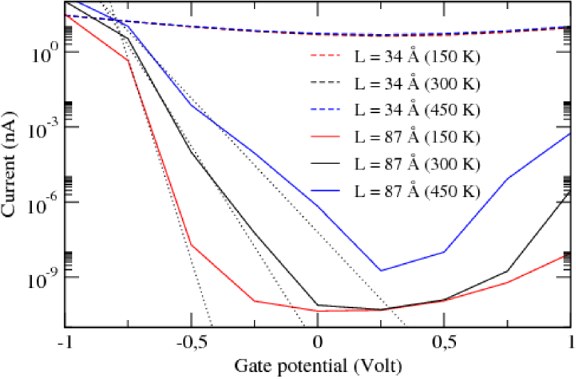
Fig. 6 also shows the electrostatic profile through the device. We see that the gate potential is almost perfectly screened by the graphene ribbon, i.e. the gate potential does not penetrate through the central ribbon. This means that for a layered structure, only the first layer would be strongly affected by the back-gate. This has some implications also for gated nanotube devices. In such a device, only the atoms facing the gate electrode will be strongly influenced, and this explains why in Ref. Sørensen et al., 2009 we found that the transport in the device was dominated by tunneling even though the nanotube was 110 Å long, and thus longer than the graphene junctions studied in this paper. Thus, to obtain efficient gating of a nanotube, the gate electrode must wrap around the tube.
VI Conclusions
In this paper we have introduced a new semi-empirical model for electron transport in nano-devices. The model is based on the Extended Hückel method that extends the work by Zahid et al.Zahid et al. (2005) to give a more complete description of the electrostatic interactions in the device. In particular, the position of the electrode Fermi level and the charge transfer between the contacts and the device are calculated self-consistently.
Compared to DFT-based transport methods, the main advantage of our new method is that it is computationally less expensive, as well as having the option of adjusting parameters to reproduce experimental data or computationally very demanding many-body electronic structure methods.
The model includes a self-consistent Hartree potential which takes into account the effect of an external bias as well as continuum dielectric regions and external electrostatic gates.
We used the model to study a Tour wire between gold electrodes, and found that the voltage drop in the device compares well with ab initio results, while the calculated current–voltage characteristics qualitatively agree better with experimental findings than the corresponding DFT-LDA results do.
We also considered a graphene nano-transistor, and our study illustrated how the transport mechanism changes from tunnelling to thermionic emission as the device is made longer.
These applications show that the new method can give an accurate description of a broad range of nano-scale devices. With its favorable computational speed, it is a good complement to ab initio-based transport methods.
Acknowledgements.
This work was supported by the Danish Council for Strategic Research ’NABIIT’ under Grant No. 2106-04-0017, “Parallel Algorithms for Computational Nano-Science”, and European Commission STREP project No. MODECOM “NMP-CT-2006-016434”, EU.References
- Haug and Jauho (1996) H. Haug and A.-P. Jauho, Quantum Kinetics in Transport and Optics of Semiconductors (Berlin Springer Verlag, 1996).
- Lang (1995) N. D. Lang, Phys. Rev. B, 52, 5335 (1995).
- Xue (2002) Y. Xue, Chemical Physics, 281, 151 (2002).
- Brandbyge et al. (2002) M. Brandbyge, J.-L. Mozos, P. Ordejón, J. Taylor, and K. Stokbro, Phys. Rev. B, 65, 165401 (2002).
- Taylor et al. (2001) J. Taylor, H. Guo, and J. Wang, Phys. Rev. B, 63, 245407 (2001).
- Di Carlo (2002) A. Di Carlo, Physica B, 314, 211 (2002).
- Pecchia and Di Carlo (2004) A. Pecchia and A. Di Carlo, Reports in Prog. in Phys., 67, 1497 (2004).
- Magoga and Joachim (1997) M. Magoga and C. Joachim, Phys. Rev. B, 56, 4722 (1997).
- Corbel et al. (1999) S. Corbel, J. Cerda, and P. Sautet, Phys. Rev. B, 60, 1989 (1999).
- Cerdá and Soria (2000) J. Cerdá and F. Soria, Phys. Rev. B, 61, 7965 (2000).
- Emberly and Kirczenow (2001) E. G. Emberly and G. Kirczenow, Phys. Rev. B, 62, 10451 (2001).
- Zahid et al. (2005) F. Zahid, M. Paulsson, E. Polizzi, A. W. Ghosh, L. Siddiqui, and S. Datta, J. of Chem. Phys., 123, 064707 (2005).
- Kienle et al. (2006) D. Kienle, J. I. Cerda, and A. W. Ghosh, J. Appl. Phys., 100, 043714 (2006a).
- Kienle et al. (2006) D. Kienle, K. H. Bevan, G.-C. Liang, L. Siddiqui, J. I. Cerda, and A. W. Ghosh, J. Appl. Phys., 100, 043715 (2006b).
- Whangbo and Hoffmann (1978) M. H. Whangbo and R. Hoffmann, J. Chem. Phys., 68, 5498 (1978).
- Pople and Segal (1966) J. A. Pople and G. A. Segal, J. Chem. Phys, 44, 3289 (1966).
- Murell and Harget (1972) J. N. Murell and A. J. Harget, Semi-empirical SCF Theory of Molecules (Wiley, 1972).
- Todorov et al. (2000) T. N. Todorov, J. Hoekstra, and A. P. Sutton, Philos. Mag. B, 80, 421 (2000).
- Datta (1997) S. Datta, Electronic Transport in Mesoscopic Systems (Cambridge University Press, Cambridge, UK, 1997).
- Kushmerick et al. (2002) J. G. Kushmerick, D. B. Holt, J. C. Yang, J. Naciri, M. H. Moore, and R. Shashidhar, Phys. Rev. Lett., 89, 86802 (2002).
- Taylor et al. (2002) J. Taylor, M. Brandbyge, and K. Stokbro, Phys. Rev. Lett., 89, 138301 (2002).
- (22) The transport calculations where performed with Atomistix ToolKit, version 2008.10. The manual is available online at http://www.quantumwise.com/documents/manuals.
- Ammeter et al. (1978) J. H. Ammeter, H. B. Burgi, J. C. Thibeault, and R. Hoffmann, J. Am. Chem. Soc., 100, 3686 (1978).
- Thygesen and Jacobsen (2005) K. S. Thygesen and K. W. Jacobsen, Phys. Rev. B, 72, 033401 (2005).
- Yan et al. (2007) Q. Yan, B. Huang, J. Yu, F. Zheng, J. Zang, J. Wu, B.-L. Gu, F. Liu, and W. Duan, Nano Letters, 7, 1489 (2007).
- Sørensen et al. (2009) H. H. B. Sørensen, P. C. Hansen, D. E. Petersen, S. Skelboe, and K. Stokbro, Phys. Rev. B, 79, 205332 (2009).