Implementation of classical logic gates at nano-scale level using magnetic quantum rings: A theoretical study
Abstract
We explore the possibilities of designing classical logic gates at nano-scale level using magnetic quantum rings. A single ring is used for designing OR, NOT, XOR, XNOR and NAND gates, while AND and NOR gate responses are achieved using two such rings and in all the cases each ring is threaded by a magnetic flux which plays the central role in the logic gate operation. We adopt a simple tight-binding Hamiltonian to describe the model where a magnetic quantum ring is attached to two semi-infinite one-dimensional non-magnetic electrodes. Based on single particle Green’s function formalism all the calculations which describe two-terminal conductance and current through the quantum ring are performed numerically. The analysis may be helpful in fabricating mesoscopic or nano-scale logic gates.
pacs:
73.63.-b, 73.63.Rt, 81.07.NbI Introduction
Discovery of giant magnetoresistance effect in Fe/Cr magnetic multilayers gmr in 1988 ignited the idea of possibility to control and manipulate electron spin degree of freedom for storage and transfer of information as in conventional electronics. With the rapid progress in nanolithography and nanofabrication techniques nanofab1 ; nanofab2 spin dependent transport at mesoscopic length scale is being paid much attention today from theoretical as well as experimental point of view due to its potential application in nanoscience and nanotechnology. Getting introduced in 1996 by S. Wolf ‘Spintronics’ wolf has outgrown as one of the most enriched and sophisticated areas in condensed matter physics over the past two decades revolutionizing the concept of information storage technology. It holds future promises to integrate memory and logic into a single device. The key idea of designing spin dependent nano-electronic devices is based on the concept of quantum interference effect imry1 , and it is generally preserved throughout the sample having dimension smaller or comparable to the phase coherence length. Therefore, ring type conductors or two path devices are ideal candidates where the effect of quantum interference can be exploited bohm . In such a ring shaped geometry, quantum interference effect can be controlled by several ways, and most probably, the effect can be regulated significantly by tuning the magnetic flux, the so-called Aharonov-Bohm (AB) flux, that threads the ring. A magnetic quantum ring penetrated by a magnetic flux yields a flux dependent spin transmission probability which may be useful for modeling of spin based logic gates and spin transistors.
In recent times, spin dependent transport through magnetic systems of ring shaped geometries has drawn much attention since these simple looking systems can be used to demonstrate several physical phenomena such as, many body correlation effect manybody , quantum phase transition qphase , resonant tunneling resonant1 ; resonant2 , spin related conductance modulation condmod , spin filtering filter , spin detecting detect , etc. At the same time, much interest has also been shown in the study of spin based transport through a quantum ring in presence of an inhomogeneous magnetic field. It provides us how such a system can used to make a device of spin switch frus ; jia and opens up the possibility of designing spin filters bird , spin transistors das , and quantum information processing imam . In a very recent work Brataas et al. brat have shown that in mesoscopic rings a spatially inhomogeneous spin-orbit (SO) interaction enhances the spin-interference effects and the transport mechanism can be understood in terms of the AB physics with fictitious spin dependent magnetic fluxes. The inhomogeneous SO interaction controls and enhances spin injection in two-terminal rings significantly and these aspects can be used for quantum computation.
Following a brief introduction of spin dependent transport through a magnetic quantum ring threaded by an AB flux , in the present work we will explore how such a quantum ring can be used for implementing classical logic gates. A single mesoscopic ring is used to design OR, NOT, XOR, XNOR and NAND gates, while AND and NOR gates are fabricated with the help of two such quantum rings. For all these logic gates, AB flux enclosed by a ring plays the central role and it controls the interference condition of electronic waves passing through two arms of the ring. Within a non-interacting picture, a tight-binding framework is used to describe the model and all the calculations are done based on single particle Green’s function technique tho ; san1 ; lee ; san2 ; ando ; san3 ; guo ; san4 . There are also several other methods like mode matching techniques modematch1 ; modematch2 ; modematch3 , transfer matrix method transfer1 ; transfer2 ; transfer3 ; transfer4 ; transfer5 , etc., those are used to study spin dependent transport in low-dimensional model quantum systems. The logical operations are addressed by studying two-terminal conductance as a function of energy and current as a function of applied bias voltage. Our numerical analysis clearly supports the logical operations of the traditional macroscopic logic gates. To the best of our knowledge, the logic gate operations using such a simple magnetic quantum ring have not been described earlier in the literature.
The organization of the paper is as follows. With a brief introduction given in Section I, in Section II we illustrate the theoretical formulation of spin dependent transport through a magnetic system sandwiched between two one-dimensional (D) semi-infinite non-magnetic (NM) metallic electrodes. The system between two electrodes can be anything like a D magnetic chain, an array of quantum dots have finite magnetic moments, a magnetic quantum ring, etc. In Section III, we present our numerical results which describe conductance-energy and current-voltage characteristics. At the end, summary of our results will be available in Section IV.
II Synopsis of the theoretical formulation
Let us start by referring to Fig. 1. A magnetic quantum ring penetrated by an AB flux is attached symmetrically to two semi-infinite D non-magnetic metallic electrodes to form a bridge system, the so-called electrode-conductor-electrode bridge. Filled red circles correspond to the positions of magnetic sites in the ring. The strength of the localized magnetic moment associated with each
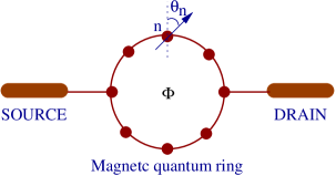
magnetic site (say) is described by the parameter and its (magnetic moment) orientation is specified by the polar angle and azimuthal angle in spherical polar coordinate system. Applying an external magnetic field, orientation of a local magnetic moment can be changed. The magnetic quantum ring with atomic sites is attached symmetrically to two D semi-infinite non-magnetic metallic electrodes, namely, source and drain having chemical potentials and under the non-equilibrium condition when bias voltage is applied. Described by the discrete lattice model, the electrodes are assumed to be composed of infinite non-magnetic sites labeled as , , , , for the left electrode and , , , , for the right one.
The Hamiltonian for the full system can be written as,
| (1) |
where, represents the Hamiltonian for the magnetic quantum ring (MQR). and correspond to the Hamiltonians for the source and drain, respectively, and is the Hamiltonian describing the ring-electrode coupling strength.
The spin polarized Hamiltonian for the MQR can be written in non-interacting electron picture within the framework of tight-binding formulation in Wannier basis, using nearest-neighbor approximation as,
| (2) |
where,
First term of Eq. 2 represents the effective on-site energies of
the atomic sites in the ring. ’s are the site energies, while
the term describes the interaction of the
spin of the injected electron to the localized on site
magnetic moments. On site flipping of spins is described mathematically
by this term. Second term describes the nearest-neighbor hopping strength
between the sites of the quantum ring, modified due to the presence of AB
flux which is incorporated by the term .
Similarly, the Hamiltonian for the two electrodes can be written as,
| (3) |
where, ’s are the site energies of source (drain) and is the hopping strength between the nearest-neighbor sites of source (drain).
Here also,
The ring-electrode coupling Hamiltonian is described by,
| (4) |
where, being the ring-electrode coupling strength.
In order to calculate the spin dependent transmission probabilities and current through the magnetic quantum ring, we use single particle Green’s function technique. Within the regime of coherent transport and for non-interacting systems this formalism is well applied.
The single particle Green’s function representing the full system for an electron with energy is defined as,
| (5) |
where,
| (6) |
being the energy of the electron passing through the system. is a small imaginary term added to make the Green’s function non-hermitian.
Now and representing the Hamiltonian and the Green’s function for the full system can be partitioned like datta1 ; datta2 ,
| (7) |
| (8) |
where, , , and represent the Hamiltonians (in matrix form) for source, quantum ring and drain, respectively. and are the matrices for the Hamiltonians representing the ring-electrode coupling strength. Assuming that there is no coupling between the electrodes themselves, the corner elements of the matrices are zero. A similar definition goes for the Green’s function matrix as well.
Our first goal is to determine (Green’s function for the ring only) which defines all physical quantities of interest. Following Eq. 5 and using the block matrix form of and the form of can be expressed as,
| (9) |
where, and represent the contact self-energies introduced to incorporate the effects of semi-infinite electrodes coupled to the system, and, they are expressed by the relations datta1 ; datta2 ,
| (10) |
Thus the form of self-energies are independent of the nano-structure itself through which transmission is studied and they completely describe the influence of electrodes attached to the system. Now, the transmission probability of an electron with energy is related to the Green’s function as,
| (11) | |||||
where, , and . Here, and are the retarded and advanced single particle Green’s functions (for the MQR only) for an electron with energy . and are the coupling matrices, representing the coupling of the magnetic quantum ring to the source and drain, respectively, and they are defined by the relation datta1 ; datta2 ,
| (12) |
Here, and are the retarded and advanced self-energies, respectively, and they are conjugate to each other. It is shown by Datta et al. that the self-energy can be expressed as a linear combination of real and imaginary parts in the form,
| (13) |
The real part of self-energy describes the shift of the energy levels and the imaginary part corresponds to broadening of the levels. The finite imaginary part appears due to incorporation of the semi-infinite electrodes having continuous energy spectrum. Therefore, the coupling matrices can be easily obtained from the self-energy expression and is expressed as,
| (14) |
Considering linear transport regime, conductance is obtained using Landauer formula datta1 ; datta2 ; land1 ; land2 ; land3 ,
| (15) |
Knowing the transmission probability of an electron injected with spin and transmitted with spin , the current through the system is obtained using Landauer-Büttiker formalism. It is written in the form datta1 ; datta2 ; land1 ; land2 ; land3 ,
| (16) |
where, gives the Fermi distribution function of the two electrodes having chemical potentials . is the equilibrium Fermi energy and is the applied bias voltage. Here we make a realistic assumption that the entire voltage is dropped across the ring-electrode interfaces, and it is examined that under such an assumption the current-voltage (-) characteristics do not change their qualitative features significantly.
III Numerical results and discussion
We start analyzing our results by mentioning the values of different parameters used for the numerical calculations. For a magnetic quantum ring, we set the on-site energy and nearest-neighbor hopping strength . Magnitude of the local magnetic moment , associated with each atomic site of the ring, is fixed at . On the other hand, for two non-magnetic electrodes the on-site energy is taken as and nearest-neighbor hopping integral is chosen as . The equilibrium Fermi energy is fixed at . For our illustrative purposes, we simplify the unit system by choosing . Energy scale is fixed in unit of .
In a bridge system (i.e., where a conductor is sandwiched between two electrodes), transport properties are significantly influenced by the conductor-to-electrode coupling strength (). To emphasize it, we describe our results for the two limiting cases depending on the coupling strength of the conductor (magnetic quantum ring) to the side attached NM electrodes. We define these two regimes as follows. Case 1: Weak-coupling limit This regime is typically defined by the condition . Here, we choose the values of the hopping parameters as .
Case 2: Strong-coupling limit This limit is described by the condition . In this regime we set the values of hopping strengths as .
In order to understand the basic mechanisms of designing classical logic gates using magnetic quantum rings, let us first discuss the spin dependent transport through a magnetic quantum ring, penetrated by an AB flux , which is symmetrically coupled to two non-magnetic metallic electrodes (for instance see Fig. 1).
III.1 A magnetic quantum ring
III.1.1 Conductance-energy characteristics
As representative examples, in Fig. 2 we display the variations of up spin conductances as a function of injecting electron energy for a magnetic quantum ring considering . The local moments associated with the magnetic atoms in two arms of the ring are aligned along direction i.e., for all . The golden yellow and sky blue lines represent the results for the weak and strong ring-to-electrode coupling limits, respectively. In the limit of weak-coupling when AB flux is not given to the ring, conductance shows fine resonant peaks (Fig. 2(a)) for some typical energy values, while for all other energies it almost drops to zero. At resonances, conductance approaches to unity, and therefore, the transmission probability becomes since we get the relation from the Landauer conductance formula (see Eq. 15) in our chosen unit . reveals a ballistic transmission through the MQR. Each resonant peak in the conductance spectrum is associated with a particular energy eigenvalue of the ring. Thus, from the conductance-energy spectrum, nature of the energy eigenvalues of the quantum ring can be directly implemented. The sharpness of resonant peaks drastically changes in the limit of strong ring-electrode coupling which is clearly visible from the sky blue curve of Fig. 2(a).
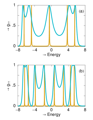
In this strong-coupling limit, all resonant peaks get broadened where the contribution for the broadening comes from the imaginary parts of the self-energies and datta1 ; datta2 . These results predict that in the limit of weak-coupling a fine tuning in energy scale is required to get spin transmission across the ring, while for the strong-coupling limit since conduction takes place in a wide range of energy, fine tuning is not necessary to get electron conduction. This coupling effect provides an important signature in the study of electron transport and the effect becomes much clearer from our current-voltage (-) characteristics. In the presence of AB flux , more resonant peaks appear in the conductance spectrum compared to the case when . The results are shown in Fig. 2(b) where we set . Appearance of more resonant peaks is associated with the existence of more discrete energy levels which is caused by removal of energy degeneracies in the presence of .
All the results presented above (Fig. 2) are associated with the variation of only up spin conductance as a function of energy . The conductance-energy spectrum for a down spin electron is exactly mirror symmetric to the spectrum observed for an up spin electron, and accordingly, we do not plot the results further for down spin electrons. This mirror symmetric like feature is observed only when we set the site energy of the MQR to zero. In addition, it is also important to note that for this MQR where all moments are aligned along direction, no spin flip transmission takes place i.e., . The explanation of zero transmission probability for spin flipping is given as follow. Spin flip occurs due to the presence of the term in the Hamiltonian (see Eq. 2), being the Pauli spin matrix with components , and for the injecting electron. The spin flipping is caused because of the operators and , respectively. For the local magnetic moments oriented along axes, becomes equal to . Accordingly, the Hamiltonian does not contain and and so as and , which provides zero flipping for up or down orientation of magnetic moments.
III.1.2 Variation of conductance with AB flux
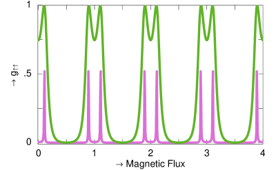
In Fig. 3 we show the dependence of up spin conductances as a function of AB flux for a magnetic quantum ring considering where all moments are aligned along direction. The magenta and green curves correspond to the up spin conductances for the weak- and strong-coupling limits, respectively, and these conductances are determined at the typical energy . It is observed that the up spin conductance in the case of weak-coupling is significantly reduced compared to the strong-coupling one, and, both for these two coupling cases up spin conductance varies periodically with showing ( in our chosen unit ) flux-quantum periodicity. Quite interestingly we notice that at , where is an odd integer, conductance drops exactly to zero. This vanishing behavior can be explained as follows.
For a symmetrically connected ring, the wave functions passing through the upper and lower arms of the ring are given by,
| (17) |
where, and are used to indicate two different paths of electron propagation along the two arms of the ring. denotes the wave function in the absence of magnetic flux and it is same for both upper and lower arms as the ring is symmetrically coupled to the electrodes. is the vector potential associated with the
magnetic field by the relation . Hence the probability amplitude of finding the electron passing through the ring can be calculated as,
| (18) |
where, is the flux enclosed by the ring.
It is clearly observed from Eq. 18 that at , where stands for an odd integer, the transmission probability of an electron exactly drops to zero irrespective of the energy . For any other values of , electron conduction no longer vanishes for the entire energy range and we get resonant peaks at the appropriate energy values. On the other hand, for an asymmetrically connected MQR, the vanishing behavior of conductance for the entire energy range at odd integer multiples of will not be observed, since in this case the wave amplitudes for the waves passing through the upper and lower arms are not identical to each other. These aspects can be utilized to design all possible logic gates which we will describe in the forthcoming sub-sections.
III.1.3 Current-voltage characteristics
All the basic features of spin dependent transport obtained from conductance-energy spectra of the magnetic quantum ring can be understood in a better way from our current-voltage characteristics. The current passing through the ring is determined by integrating the transmission function according to Eq. 16, where the transmission function varies exactly similar to that of the conductance spectrum apart from a scale factor (see Eq. 15), which is equal to in our chosen unit system .
As illustrative examples, in Fig. 4 we present the variations of up spin currents as a function of applied bias voltage for a symmetrically connected magnetic quantum ring where all moments are aligned along direction. Here we fix so that each arm of the ring contains magnetic sites. The reddish-yellow and blue curves represent the currents for and , respectively.
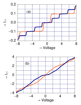
In the limit of weak-coupling, current shows step-like behavior as a function of bias voltage (Fig. 4(a)), where each step is associated with a sharp resonant peak in the conductance-energy spectrum. With the increment of bias voltage , electrochemical potentials and in the two electrodes shift gradually and eventually cross one of the quantized energy levels of the MQR, and therefore, a current step appears in the current-voltage characteristic curve. The effect of AB flux is quite interesting and it can be understood clearly by noting the curves presented in Fig. 4(a). In presence of () more steps appear in the current-voltage characteristic curve (blue line) associated with the conductance-energy spectrum, compared to the case when is set to zero (reddish-yellow line). With this feature it also important to note that the typical bias voltage where electron starts to conduct through the electrode-ring-electrode bridge, the so-called threshold voltage , can be regulated significantly through the AB flux . As increases towards from value, gets increased gradually, and, at the typical value of , is maximum where electron conduction is stopped for the complete range of bias voltage. This phenomenon can be utilized in designing nano-electronic devices.
The step-like behavior almost disappears in the case of strong ring-to-electrode coupling limit, as shown in Fig. 4(b), where the reddish-yellow and blue curves correspond to the identical meaning as in Fig. 4(a). Here the current amplitude is very high compared to the weak-coupling limit. This continuous like feature with large current amplitude can be easily explained from the conductance-energy spectrum discussed earlier. Thus, in short we can say that for a fixed bias voltage, current amplitude can be controlled by tuning the ring-electrode coupling strength.
In the following sub-sections we will try to explore how these features of spin dependent transmission through a MQR can be implemented to fabricate several classical logic gates. We will describe two-input logic gates where the inputs are associated with externally applied magnetic fields through which we can tune the orientation of local magnetic moments in the magnetic atomic sites. Throughout our discussion we mention the two inputs in terms of polar angles (expressed by the symbol ) of two magnetic moments associated with applied gate magnetic fields. For all logic gate operations AB flux plays the central role and we fix it at i.e., in our chosen unit system.
III.2 OR gate
Let us start with OR gate response. The schematic view of a magnetic
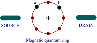
quantum ring that can be used as an OR gate is shown in Fig. 5. The ring, penetrated by an AB flux , is symmetrically coupled to two semi-infinite D non-magnetic metallic electrodes, namely, source and drain. Two magnetic sites and in upper arm of the ring are subject to two external gate magnetic fields through which the orientations and of local magnetic moments associated with the respective sites and are controlled, and these two ( and ) are treated as two inputs of the OR gate. Quite interestingly we observe that, at a high output current () (in the logical sense) appears if one or both the inputs to the gate are high (), while if neither input is high (), a low output current () appears. This phenomenon is the so-called OR gate response and here we address it by studying conductance-energy and current-voltage characteristics as functions of magnetic flux and gate magnetic fields.
As illustrative examples in Fig. 6 we plot up spin conductances
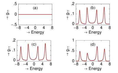
as a function of injecting electron energy for a magnetic quantum ring with in the limit of strong-coupling, where (a), (b), (c) and (d) correspond to four different cases of two input signals. When both the two inputs are low () i.e., , up spin conductance vanishes for the entire energy range (Fig. 6(a)) which reveals no electron conduction through the ring. This vanishing behavior is clearly explained from our previous discussion where we have shown that, the transmission probability of an electron across a symmetrically connected ring (upper and lower lower arms are identical in nature) drops exactly to zero at the typical flux . With this argument we can justify the vanishing nature of up spin conductance for the particular case when . Since in such a case the upper and lower arms are exactly identical to each other as we set for all except and , and accordingly, zero transmission probability is achieved for the entire range of energy . On the other hand, when the symmetry between the two arms of the ring is broken by applying an external magnetic field to anyone of the two input gates i.e., and (Fig. 6(b)) or and (Fig. 6(c)) or by applying external magnetic fields in both the two input gates i.e., (Fig. 6(d)), up spin conductance shows resonant peaks for some particular energies associated with the energy eigenvalues of the magnetic quantum ring.
In addition we also observe that in the cases where anyone of the two inputs to the gate is high and other is low, the height of the resonant peaks gets reduced compared to the case where both inputs are high. This is solely due to the effect of quantum interference among the electronic waves passing through two arms of the ring. From these conductance-energy spectra we can predict that electron conduction through the ring takes place when anyone or both the inputs to the gate are high (), while for the case where both inputs are low electron conduction is no longer possible. It emphasizes the OR gate behavior. In the above conductance-energy spectra (Figs. 6(a)-(d)), we display the variation of up spin conductance as a function of energy depending on the four different choices of two input signals. An exactly similar kind of behavior (OR gate response) will be also observed for down spin electrons, where conductance-energy spectrum gets mirror symmetric like nature compared to up spin electrons. But, no spin flip transmission in these four different configurations takes place i.e., and are always zero as the moments are aligned along directions.
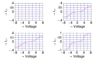
Following the above conductance-energy spectra now we describe the current-voltage characteristics. In Fig. 7 we plot the variations of up spin currents as a function of applied bias voltage for the magnetic quantum ring () in the limit of strong-coupling, where (a), (b), (c) and (d) represent the results for the four different choices of two inputs and . When both inputs are low i.e., , current vanishes for the entire range of bias voltage (Fig. 7(a)). This is clearly explained from Fig. 6(a), since current is evaluated by integrating the transmission function. While, in other three cases of two input signals i.e., and (Fig. 7(b)), and (Fig. 7(c)) and (Fig. 7(d)), up spin current shows a quite continuous variation with the bias voltage , following the conductance-energy spectra (Figs. 6(b)-(d)).
| Input-I () | Input-II () | Current (I) |
Associated with the quantum interference effect among the two arms of the ring, the larger current amplitude for a fixed bias voltage in the typical case where two inputs are high (Fig. 7(d)) compared to the cases where one input is high and other is low (Figs. 7(b)-(c)) is clearly understood. These characteristics demonstrate that a magnetic quantum ring can be used as an OR gate.
To be more precise, we make a quantitative estimate of the typical current amplitude, given in Table 1, where the current amplitude is measured at the bias voltage . It shows that when both inputs are high (), current gets the value and for the cases where anyone of the two inputs is high and other is low (), current becomes . On the other hand, current is zero for the particular case where both inputs are low. These aspects reveal the OR gate response in a magnetic quantum ring.
III.3 AND gate
To design an AND logic gate we use two similar magnetic quantum rings those are directly coupled to each other via a single bond. The schematic view of the double quantum ring that can be used as an AND gate is presented in Fig. 8, where individual rings are penetrated by an AB flux . The double quantum ring is then attached symmetrically to two semi-infinite D metallic electrodes, namely, source and drain. Two magnetic sites and in upper arms of the two rings are subject
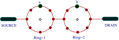
to two external gate magnetic fields through which the orientations of local magnetic moments and in sites and are controlled. We consider them ( and ) as the two
inputs of the AND gate. We will show that, at the typical flux , a high output current () (in the logical sense) appears only if both the two inputs to the gate are high (), while if neither or only one input to the gate is high (), a low output current () results. It is the so-called AND gate response and we investigate it by studying conductance-energy and current-voltage characteristics.
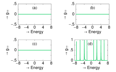
To explore AND gate response, first we describe conductance-energy characteristics. In Fig. 9 we show the variations of up spin conductances () as a function of energy in the limit of strong-coupling for a double quantum ring with () magnetic sites, where (a), (b), (c) and (d) represent the results for different choices of input signals and .
It is observed that when both and are identical to zero (low), up spin conductance vanishes throughout the energy range (Fig. 9(a)). The reason is that, by making two inputs to zero the upper and lower arms of individual rings are similar in nature, and therefore, their contributions to the transmission probability disappear at the typical flux . A similar kind of vanishing behavior of up spin conductance in the complete energy band is also observed for the two other cases where anyone of the two inputs is high and other is low. The results are shown in Figs. 9(b) and (c), where we set , and , , respectively. In these two choices of input signals, symmetry between the upper and lower arms of two rings is not broken simultaneously. When the symmetry is broken in one ring by applying a gate magnetic field, it (symmetry) is preserved in the other ring and vice versa. Now, for the asymmetric ring we get non-vanishing transmission probability, while for the symmetric ring transmission amplitude becomes zero, and therefore, as a combined effect we get vanishing transmission amplitude since two rings are directly coupled to each other. The non-zero value of up spin conductance is obtained only when the symmetry of the two rings are broken individually by applying external gate magnetic fields in the upper arms of two rings i.e., (Fig. 9(d)). Thus, from the above conductance-energy spectra we can predict that the electron conduction through the double quantum ring is possible only when both the inputs to the gate are high (), while if neither or anyone input to the gate is high, no electron conduction takes place. These features are associated with traditional AND gate response.
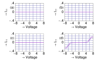
Now we go for current-voltage characteristics to reveal AND gate response in a double quantum ring. As representative examples, in Fig. 10 we plot up spin currents as a function of applied bias voltage for a double quantum ring in the strong-coupling limit, where (a), (b), (c) and (d) correspond to four different cases of two input signals. When we put two inputs identically to low value i.e., , up spin current becomes zero (Fig. 10(a)) for the full width of applied bias voltage . An exactly similar vanishing behavior of up spin current is also available for the other two cases of input signals, where only one input is high and other is low. The results are presented in Figs. 10(b) and (c).
| Input-I () | Input-II () | Current (I) |
For these three cases of the two input signals, the vanishing behavior of up spin current can be easily understood from the conductance-energy spectra given in Figs. 9(a)-(c), since current is determined by integrating the transmission function. The finite non-zero value of up spin current is available only for the typical case where both the two inputs are high i.e., (Fig. 10(d)), following the conductance curve (Fig. 9(d)). From this current-voltage curve we see that the up spin current shows non-zero value beyond a finite value of bias voltage , the so-called threshold voltage . This threshold voltage can be regulated by tuning the ring-electrode coupling strength as well as by controlling the size of the magnetic quantum ring. This characteristic provides an important signature in designing nano-electronic devices. These results support AND gate response.
In the same fashion as earlier here we also make a quantitative estimate for the typical current amplitude as given in Table 2, where the typical current amplitude is measured at the bias voltage . It shows that the current gets the value only when both the two inputs are high, while for all other cases i.e, where neither input is high or only one is high, current drops exactly zero. It simplifies the AND gate behavior in a double quantum ring.
III.4 NOT gate
Next we discuss NOT gate operation in a magnetic quantum ring. Schematic view for the operation of a NOT gate by using a single ring is shown in Fig. 11, where the ring is attached symmetrically to two semi-infinite D metallic electrodes, viz, source and drain, and
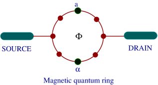
it is subject to an AB flux . Applying gate magnetic fields in the magnetic sites named as and in upper and lower arms of the ring we tune the directions of local magnetic moments and in these two respective sites. Keeping to a fixed value, we change properly to achieve the NOT gate operation. This is regarded as the input of our NOT gate. We will verify that, at the typical flux , a high output current () (in the logical sense) appears if the input to the gate is low (), while a low output current () appears when the input to the gate is high (). This phenomenon is the so-called NOT gate behavior, and we will explore it following the same prescription as earlier.
To describe NOT gate operation let us start with the conductance-energy characteristics. In Fig. 12 we show the variations of up spin conductances () as a function of injecting electron energy () for a typical magnetic quantum ring considering in the limit of strong-coupling, where (a) and (b) illustrate the results for two different choices of the input signal . Throughout this logical operation we fix to i.e., the moment in site is oriented along the direction. From our results we see that when the input to the gate is high i.e., , up spin conductance disappears for the entire band of energy (Fig. 12(b)) which reveals that for this typical case electron conduction doesn’t take place through the magnetic quantum ring. This disappearing nature of up spin conductance can be implemented as follows. The magnetic moment at the site is fixed at an angle , and thus as we tune to by applying an external gate magnetic filed i.e., the input signal is high, both upper and lower arms of the ring are exactly similar in nature. In this situation the ring contributes nothing for electron conduction at the typical AB flux . Now if is dissimilar from , then the two arms will not be identical to each other and then the transmission probability should not not vanish. Hence, to get zero transmission probability across the ring when the input signal is
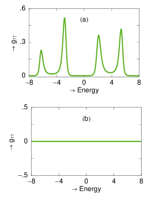
high, we should tune properly observing , and vice versa. On the other hand, for the other case where the input signal is low i.e., , up spin conductance exhibits resonant peaks at some particular energies associated with energy eigenvalues of the magnetic quantum ring. The fact is that, by making input to zero we eventually destroy the symmetry among the upper and lower arms of the ring, and accordingly, for this low input signal ring allows electrons to conduct through it. Therefore, for low input signal electron is allowed to pass through the ring, while in the case of high input electronic transmission is completely blocked. This behavior is associated with the traditional NOT gate operation.
To illustrate the current-voltage characteristics now we concentrate on the results given in Fig. 13. The up spin currents are drawn as a function of applied bias voltage for a magnetic quantum ring with in the strong-coupling limit, where (a) and (b) represent the results for two choices of the input signal . When i.e., high input, up spin current vanishes throughout the bias voltage . The result is given in Fig. 13(b) and for this input signal the vanishing nature is clearly followed from the conductance-energy spectrum shown in Fig. 12(b). While, for the case of low input i.e., , current gets a finite value (Fig. 13(a))
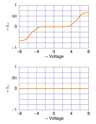
following the conductance spectrum (Fig. 12(a)). Here, the current becomes non-zero beyond a threshold voltage which is tunable depending on the ring size and ring-electrode coupling strength.
| Input () | Current () |
|---|---|
From these current-voltage curves it is clear that a high output current appears only if the input to the gate is low, while for high input current doesn’t appear. It justifies NOT gate response in the magnetic quantum ring.
In a similar way, as we have studied earlier in other logic gates, in Table 3 we make a quantitative measurement of the typical current amplitude for the magnetic quantum ring. The current amplitude is computed at the bias voltage . It provides that the current gets the value when input is low, while it (current) goes to zero as we set the input to the high value. Thus the NOT gate operation by using a magnetic quantum ring is established.
Up to now we have studied three primary logic gate operations using one (OR and NOT) and two (AND) magnetic quantum rings. In the forthcoming sub-sections we will explore the other four combinatorial logic gate operations using such one or two magnetic quantum rings.
III.5 NOR gate
Let us begin with NOR gate operation. Like an AND gate, here we also use two identical magnetic quantum rings to design a NOR gate. The model quantum system is schematically shown in Fig. 14, where two magnetic quantum rings, namely, ring-1 and ring-2, are directly coupled to each other through a single bond and individual rings are threaded by an AB flux . The double quantum ring is then attached symmetrically to two semi-infinite D metallic electrodes, viz, source and drain. In the upper and lower arms of these two rings we choose four magnetic sites referred as , , and where external magnetic
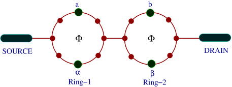
fields are applied to tune the orientations , , and of local magnetic moments in these four respective sites. Keeping and to specific values, we regulate and properly to achieve NOR gate operation and we call these two ( and ) as the two inputs of our NOR gate. Quite nicely we establish that, at the typical AB flux , a high output current () (in the logical sense) appears if both the inputs to the gate are low (), while if one or both are high (), a low output current () results. This phenomenon is the so-called NOR gate response and we will illustrate it by describing conductance-energy and current-voltage characteristics.
As illustrative examples in Fig. 15 we present the variations of up spin conductances as a function of injecting electron energy for a double quantum ring in the limit of strong ring-to-electrode coupling, where (a), (b), (c) and (d) correspond to four different cases of two input signals. The ring sizes are fixed at and the magnetic moments in and sites are rotated by an angle with respect to preferred direction, and, throughout this logical operation we fix these two moments in such a way. From the conductance-energy characteristics we see that, up spin conductance contributes nothing when both the two inputs to the gate are set as high i.e., (Fig. 15(d)). The vanishing behavior of up spin conductance for this particular choice of input signals can be justified as follows. Initially, the magnetic moments in sites and of lower arms of ring-1 and ring-2 are fixed at an angle .
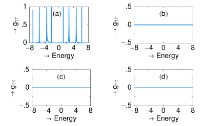
Hence, by applying external magnetic fields in the sites and as we tune and to , the upper and lower arms of individual rings are exactly similar in nature. In this situation individual rings contribute nothing to the transmission probability at the typical flux which provides our desired result. A similar kind of vanishing nature of up spin conductance is also observed in the other two cases where one input is high and other is low. The results are shown in Fig. 15(b) ( and ) and in Fig. 15(c) ( and ). In these two choices of input signals, the situation is quite different from the particular case where both inputs are high. Here, the symmetry is broken by applying an external magnetic filed which provides non-zero contribution to the transmission probability, while it (symmetry) is maintained by setting one input to low value which gives zero contribution. Therefore, the net contribution to the transmission probability becomes zero as the two rings are directly coupled to each other. The non-zero value of up spin conductance is achieved only when the symmetries among upper and lower arms of the two rings are broken individually. It takes place when both the inputs to the gate are low i.e., (Fig. 15(a)). Thus, in short we can say that the electron
conduction through the double quantum ring takes place only if both the inputs to the gate are low, while if anyone or both are high, electron transmission from the source to drain is forbidden. These
| Input-I () | Input-II () | Current (I) |
features agree well with conventional NOR gate operation.
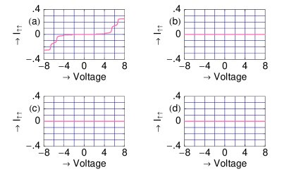
To support the NOR gate operation now we focus our mind on the current-voltage characteristics. As representative examples, in Fig. 16 we display the variations of up spin currents with bias voltage for a double quantum ring choosing , in the limit of strong ring-to-electrode coupling, where (a), (b), (c) and (d) correspond to four different cases of two input signals and . From the current-voltage spectra we observe that up spin current disappears for the full width of bias voltage when either both the two inputs to the gate are high (Fig. 16(d)) or one is high and other is low (Figs. 16(b)-(c)). This vanishing character of up spin current is followed from the conductance-energy spectra as illustrated in Figs. 15(b)-(d). The non-vanishing feature of the current is available only when both the two inputs are low (Fig. 16(a)), obeying the conductance-energy curve plotted in Fig. 15(a). At much low bias voltage, current is almost zero and it shows a finite value beyond a threshold voltage depending on the ring size and ring-to-electrode coupling strength. These features establish the NOR gate response.
For the sake of our completeness, in Table 4 we do a quantitative measurement of typical current amplitude, determined at the bias voltage , for the four different choices of two input signals in the limit of strong-coupling. Our measurement shows that the current gets a finite value () only when both inputs are low (). On the other hand, the current becomes zero for all other cases i.e., if one or both inputs are high. Therefore, it is manifested that a double quantum ring can be used as a NOR gate.
III.6 XOR gate
As a follow up, now we address XOR gate response which is designed by using a single magnetic quantum ring. The ring, penetrated by an AB flux

, is attached symmetrically to two semi-infinite D non-magnetic metallic electrodes, namely, source and drain. Our model quantum system is schematically shown in Fig. 17. Two magnetic sites, named as and , in upper and lower arms of the ring are subject to external magnetic fields through which we can regulate the orientations and of local magnetic moments in these respective sites, and, these two ( and ) are taken as the two inputs of our XOR gate. Very nicely we follow that, at the typical AB flux , a high output current () (in the logical sense) appears if one, and only one, of the inputs to the gate is high (), while if both inputs are low () or both are high (), a low output current () results. This is the so-called XOR gate behavior and we will emphasize it according to our earlier prescription.
Let us start with the conductance-energy characteristics given in Fig. 18. The variations of up spin conductances () are shown as a function of injecting electron energy for a magnetic quantum ring considering in the strong ring-to-electrode coupling limit, where four different figures correspond
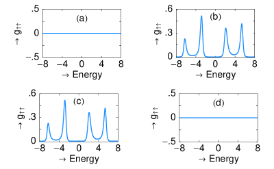
to the results for the different choices of two input signals and . It is observed that when both inputs are high i.e., , up spin conductance gets zero value in the complete energy band (see Fig. 18(d)). The reason is that for this typical case both upper and lower arms of the ring are exactly similar in nature, and therefore, at the AB flux transmission probability across the rings becomes zero for any energy of the source electron. An exactly identical response of up spin conductance is also visible for the typical case where both inputs are low i.e., (Fig. 18(a)) and this vanishing nature can be implemented according to the same prescription as for the case high inputs. The non-zero value of up spin conductance is obtained only when the symmetry among the two arms is broken and it can be done by setting one input to high and other to low. The results are shown in Figs. 18(b) and (c), where we set , and , , respectively. Therefore, from these conductance-energy spectra we can predict that the electron can allowed to pass through the magnetic quantum ring provided anyone
input to the gate is high () and other is low (), while for all other cases i.e., if both inputs are either high or low, transmission of an electron through the ring becomes forbidden for any energy . This phenomenon illustrates the traditional XOR gate response.
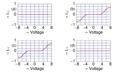
With these conductance-energy spectra (Fig. 18), now we focus our attention on the current-voltage characteristics. As illustrative
| Input-I () | Input-II () | Current (I) |
purposes in Fig. 19 we plot up spin currents as a function of applied bias voltage for a typical magnetic quantum ring considering in the limit of strong ring-to-electrode coupling, where (a)-(d) represent the results for the four different choices of input signals and . Our results show that up spin current contributes nothing as long as both inputs to the gate are set as low () or high (). For the case of low inputs, result is shown in Fig. 19(a), while in Fig. 19(d) the result is given when both inputs are high. In these two cases, the vanishing nature of the current is justified from our conductance-energy spectra given in Figs. 18(a) and (d). On the other hand, for other choices of two input signals current shows non-zero value (Figs. 19(b) and (c)), following the conductance spectra (Figs. 18(b) and (c)). The finite value of up spin current appears when the applied bias voltage crosses a limiting value, which is the so-called threshold bias voltage . Thus to get a current across the ring, we have to take care about the threshold voltage. These results implement the XOR gate response in a magnetic quantum ring.
To make an end of the discussion for XOR gate response in a more compact way in Table 5 we make a quantitative measurement of typical current amplitude for the four different cases of two input signals. The current amplitudes are computed at the bias voltage . It is observed that current becomes zero when both inputs are either low or high. While, it (current) reaches the value when we set one input as high and other as low. These studies suggest that a magnetic quantum ring can be used as a XOR gate.
III.7 XNOR gate
As a consequence now we will explore XNOR gate response and we design this logic gate by means of a single magnetic quantum ring. The ring, threaded by an AB flux , is attached symmetrically to two semi-infinite D non-magnetic metallic electrodes, namely, source and drain.
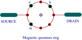
The model quantum system is schematically shown in Fig. 20. Two magnetic sites specified as and situated in the upper arm and one magnetic site named as placed in the lower arm of the ring are subject to external gate magnetic fields through which the orientations , and of local magnetic moments in the respective sites , and can be altered. These and are considered as the inputs of our two-input XNOR logic gate. We show that, at the typical magnetic flux a high output current () (in the logical sense) appears if both the two inputs to the gate are the same, while if one but not both inputs are high (), a low output current () results. This logical operation is the so-called XNOR gate behavior and we will focus it by studying conductance-energy spectrum and current-voltage characteristics for a typical magnetic quantum ring.
As representative examples, in Fig. 21 we show the variations of up spin conductances as a function of injecting electron energy for a typical magnetic quantum ring with and in the limit of strong ring-to-electrode coupling, where (a)-(d) correspond to the
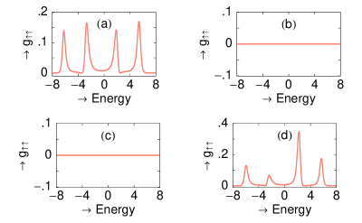
four different cases of two input signals and . From the results it is noticed that for the cases where one input is high () and other is low () i.e., , and , , up spin conductance disappears for the entire energy band (Figs. 21(b) and (c)), and therefore, for these two choices of input signals electronic transmission through the magnetic quantum ring is completely forbidden. This feature can be implemented as follows. The magnetic moment in site is rotated by an angle and throughout this logic gate operation it is aligned in such a way. Thus, as we set anyone input to high () by applying an external gate magnetic field and other to low (), upper and lower arms of the ring become exactly identical in nature to each other which provide zero transmission probability at the typical AB flux . For any other orientation of the moment placed at the site i.e., if the vanishing transmission probability will not appear for the cases where one input is set at a high value and other is fixed to a low value. Hence, to achieve zero transmission probability across the bridge, we have to fix properly considering the input signals and vice versa. For the other two cases of input signals i.e., when both the inputs are either low () or high (), non-vanishing transmission probability of up spin electrons is observed. In these two particular cases, up spin conductance shows resonant peaks (Figs. 21(a) and (d)) for some typical energies associated with the energy eigenvalues of the magnetic quantum ring. This non-vanishing nature of up spin conductance is quite obvious, since
in these two cases of input signals symmetry between two arms of the magnetic quantum ring is broken. It is also observed that the heights of the resonant peaks are very small compared to unity which is due to the effect of quantum interferences among the two arms of the ring. From these conductance-energy spectra of four different choices of input signals it can be manifested that the electronic conduction through the magnetic quantum ring is possible only when both inputs to the gate are either low () or high (). While, for all other cases electron conduction through the ring is no longer possible. This phenomenon reveals the conventional XNOR gate response.
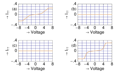
As a continuation now we follow the current-voltage characteristics to reveal XNOR gate response. In Fig. 22 we plot the variations of up spin currents as a function of applied bias voltage for a typical magnetic quantum ring with and in the strong-coupling limit, where (a)-(d) correspond to the results for the four different choices of input signals and . Following the conductance-energy spectra shown in Figs. 21(b) and (c), we see that up spin current drops to zero for any bias voltage when anyone input is fixed at a high value and other is kept at low. The results are presented in Figs. 22(b) and (c).
| Input-I () | Input-II () | Current (I) |
The finite contribution of up current is available only when the symmetry between the two arms of the ring is broken either by making two inputs zero i.e., (Fig. 22(a)), or by applying magnetic fields to the input gates i.e., (Fig. 22(d)). These current-voltage characteristics justify the XNOR gate response in a magnetic quantum ring.
To be more precise, in Table 6 we make a quantitative measurement of typical current amplitude for the different choices of two input signals in the strong ring-to-electrode coupling. The typical current amplitude is computed at the bias voltage . It is noticed that current gets the value when both inputs are low (), while it becomes when both inputs to the gate are high (). On the other hand for all other cases, current is always zero. These results emphasize that a magnetic quantum ring can be used to design a XNOR gate.
III.8 NAND gate
At the end, we demonstrate NAND gate response and we design this logic gate with the help of a single magnetic quantum ring. The ring, penetrated by an AB flux , is attached symmetrically to two semi-infinite D non-magnetic metallic electrodes, viz, source and drain. The schematic view of the magnetic quantum ring that can be used to design a NAND gate is shown in Fig. 23. In the lower arm of the ring, two magnetic sites labeled as and are subject to external magnetic
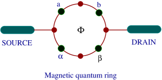
fields through which the orientations and of magnetic moments in these respective sites are altered. Throughout the NAND gate operation we set . In addition, we choose another two sites specified as and in upper arm of the ring where external magnetic fields are applied through which the orientations and of magnetic moments in these two sites are controlled. These two ( and ) are variable and they are considered as two input of the NAND gate. Quite interestingly we notice that, at the typical AB flux a high output current () (in the logical sense) appears if one or both inputs to the gate are low (), while if both inputs to the gate are high (), a low output current () results.
This characteristic is the so-called NAND gate response and we will justify it by describing the conductance-energy and current-voltage spectra.
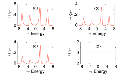
Let us begin with the results given in Fig. 24. Here we show the variations of up spin conductances as a function of injecting electron energy for a typical magnetic quantum ring with in the limit of strong ring-to-electrode coupling considering , where (a)-(d) correspond to four different choices of two input signals and . Our results predict that for the typical case when both the two inputs to the gate are high i.e., , up spin conductance disappears for the complete energy band which reveals no electronic transmission through the magnetic quantum ring (Fig. 24(d)). The reason is that, for this particular choice of two inputs, both the upper and lower arms of the ring become exactly identical in nature, and therefore, at the typical flux the ring contributes nothing to the electronic transmission probability. On the other hand, for all other possible cases of two input signals i.e., either when both the two inputs are low () or anyone is low
and other is high, up spin conductance shows resonant peaks for some particular energies associated with the energy eigenvalues of the magnetic quantum ring. The results are presented in Figs. 24(a)-(c). In these three cases, symmetry among the two arms of the ring is no longer exists, and therefore, non-zero transmission probability appears. A careful observation predicts that the heights of resonant peaks for the cases where only one input is high and other is low (Figs. 24(b)-(c)) get reduced significantly compared to the case where both inputs are low (Fig. 24(a)). This is solely due to the effect of quantum interference among the two arms of the magnetic quantum ring. Thus, from these conductance-energy spectra we can predict that the electron conduction through the ring takes place if one or both the inputs are low (), while if both are high () no electron conduction takes place across the bridge system. These results justify the traditional NAND gate operation.
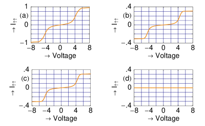
In the same fashion, now we focus on the current-voltage characteristics. As our illustrative purposes, in Fig. 25 we present the variations of up spin currents in terms of applied bias voltage for a typical magnetic quantum ring with in the limit of strong-coupling,
| Input-I () | Input-II () | Current (I) |
considering , where (a)-(d) represent the results for the different cases of two input signals. When both inputs are high i.e, up spin current becomes zero for the entire range of applied bias voltage (Fig. 25(d)), following the conductance-energy spectrum given in Fig. 24(d) since the current is determined by integrating the transmission function. For all the other three choices of two inputs, finite contribution in up spin current is available. The results are shown in Figs. 25(a)-(c). From these three current-voltage spectra, it is observed that for a fixed bias voltage current amplitude in the typical case where both inputs are low (Fig. 25(a)) is much higher than the cases where one input is high and other is low (Figs. 25(b)-(c)). This is clearly understood from the variations of conductance-energy spectra studied in the above paragraph. Thus, our present current-voltage characteristics justify the NAND gate operation in the magnetic quantum ring very nicely.
Finally, in Table 7 we present a quantitative estimate of the typical current amplitude for the four different cases of two input signals. The typical current amplitudes are measured at the bias voltage . It provides that the current vanishes when both inputs are high (). On the other hand, the current gets the value as long as both inputs are low () and when anyone of two inputs is low and other is high. Our results support that a magnetic quantum ring can be utilized as a NAND gate.
IV Concluding remarks
In the present work, we have implemented classical logic gates like OR, AND, NOT, NOR, XOR, XNOR and NAND at nano-scale level using magnetic quantum rings. A single ring is used to design OR, NOT, XOR, XNOR and NAND gates, while the rest two gates are fabricated by using two such rings and in all the cases each ring is penetrated by an AB flux which plays the crucial role for the whole logic gate operations. We have used a simple tight-binding framework to describe the model, where a magnetic quantum ring is attached to two semi-infinite one-dimensional non-magnetic metallic electrodes. Based on a single particle Green’s formalism all the calculations have been done numerically which demonstrate two-terminal conductance and current through the system. Our theoretical analysis may be useful in fabricating mesoscopic or nano-scale logic gates.
Throughout our work, we have studied seven possible logic gates. Out of which five logic gates are designed by using a single magnetic quantum ring, while the rest two are fabricated with the help of two magnetic quantum rings. In the case of single rings, we have chosen the rings with total number of atomic sites . On the other hand, for the coupled ring systems, we have considered two identical rings, where each ring contains atomic sites. In our model calculations, these typical numbers ( or ) are chosen only for the sake of simplicity. Though the results presented here change numerically with the ring size (), but all the basic features remain exactly invariant. To be more specific, it is important to note that, in real situation the experimentally achievable rings have typical diameters within the range - m. In such a small ring, unrealistically very high magnetic fields are required to produce a quantum flux. To overcome this situation, Hod et al. have studied extensively and proposed how to construct nanometer scale devices, based on Aharonov-Bohm interferometry, those can be operated in moderate magnetic fields baer4 ; baer5 ; baer6 ; baer7 .
In the present paper we have done all the calculations by ignoring the effects of temperature, electron-electron correlation, disorder, etc. Due to these factors, any scattering process that appears in the mesoscopic ring would have influence on electronic phases, and, in consequences can disturb the quantum interference effects. Here we have assumed that, in our samples all these effects are too small, and accordingly, we have neglected all these factors in this particular study.
The importance of this article is mainly concerned with (i) the simplicity of the geometry and (ii) the smallness of the size.
ACKNOWLEDGMENTS
I acknowledge with deep sense of gratitude the illuminating comments and suggestions I have received from Prof. S. N. Karmakar and Moumita Dey during the calculations.
References
- (1) M. N. Baibich, J. M. Broto, A. Fert, F. N. Van Dau, F. Petroff, P. Etienne, G. Creuzet, A. Friederich, and J. Chazelas, Phys. Rev. Lett. 61, (1998) 2472.
- (2) J. Chen, M. A. Reed, A. M. Rawlett, and J. M. Tour, Science 286, 1550 (1999).
- (3) P. Ball, Nature (London) 404, 918 (2000).
- (4) S. A. Wolf et al., Science 294, 1488 (2001).
- (5) Y. Imry, Introduction to Mesoscopic Physics, Oxford University Press, Oxford (2002).
- (6) Y. Aharonov and D. Bohm, Phys. Rev. 115, 485 (1959).
- (7) D. Boese, W. Hofstetter, and H. Schoeller, Phys. Rev. B 64, 125309 (2001).
- (8) W. Hofstetter and H. Schoeller, Phys. Rev. Lett. 88, 016803 (2001).
- (9) T. V. Shahbazyan and M. E. Raikh, Phys. Rev. B 49, 17123 (1994).
- (10) B. Kubala and J. König, Phys. Rev. B 65, 245301 (2002).
- (11) I. A. Shelykh, N. T. Bagraev, N. G. Galkin, and L. E. Klyanchkin, Phys. Rev. B 71, 113311 (2005).
- (12) H. W. Wu, J. Zhou, and Q. W. Shi, Appl. Phys. Lett. 85, 1012 (2004).
- (13) R. Ionicioiu and I. D’Amico, Phys. Rev. B 67, 041307(R) (2003).
- (14) D. Frustaglia, M. Hentschel, and K. Richter, Phys. Rev. Lett. 87, 256602 (2001).
- (15) C.-L. Jia, S.-J. Wang, H.-G. Luo, and J.-H. An, J. Phys.: Condens. Matter 16, 2043 (2004).
- (16) M. J. Gilbert and J. P. Bird, Appl. Phys. Lett. 77, 1050 (2000).
- (17) S. Datta and B. Das, Appl. Phys. Lett. 56, 665 (1990).
- (18) A. Imamoglu et al., Phys. Rev. Lett. 83, 4204 (1999).
- (19) Y. Tserkovnyak and A. Brataas, Phys. Rev. B 76, 155326 (2007).
- (20) D. J. Thouless and S. Kircpatric, J. Phys. C 14, 235 (1981).
- (21) S. K. Maiti, Solid State Commun. 149, 1623 (2009); ibid. 149, 1684 (2009); ibid. 149, 2146 (2009).
- (22) P. A. Lee and D. S. Fisher, Phys. Rev. Lett. 47, 882 (1981).
- (23) S. K. Maiti, J. Phys. Soc. Jpn. 78, 114602 (2009).
- (24) T. Ando, Phys. Rev. B 44, 8017 (1991).
- (25) S. K. Maiti, Phys. Lett. A 373, 4470 (2009).
- (26) Q. Sun, J. Wang, and H. Guo, Phys. Rev. B 71, 165310 (2005).
- (27) S. K. Maiti, Phys. Scr. 89, 055704 (2009).
- (28) G. Kirczenow, Phys. Rev. B 72, 075351 (2005).
- (29) J. A. Brum, Phys. Rev. B 43, 12082 (1991).
- (30) H. Tamura and T. Ando, Phys. Rev. B 44, 1792 (1991).
- (31) C. Pacher and E. Gornik, Physica E 21, 119 (2004).
- (32) C. Pacher and E. Gornik, Phys. Rev. B 68, 155319 (2003).
- (33) J. Heinrichs, J. Phys.: Condens. Matter 12, 5565 (2000).
- (34) B. Molnár, F. M. Peeters, and P. Vasilopoulos, Phys. Rev. B 69, 155335 (2004).
- (35) A. A. Shokri and M. Mardaani, Solid State Commun. 137, 53 (2006).
- (36) S. Datta, Electronic transport in mesoscopic systems, Cambridge University Press, Cambridge (1997).
- (37) S. Datta, Quantum Transport: Atom to Transistor, Cambridge University Press, Cambridge (2005).
- (38) R. Landauer, Phys. Lett. A 85, 91 (1986).
- (39) R. Landauer, IBM J. Res. Dev. 32, 306 (1988).
- (40) M. Büttiker, IBM J. Res. Dev. 32, 317 (1988).
- (41) O. Hod, R. Baer, and E. Rabani, J. Phys. Chem. B 108, 14807 (2004).
- (42) O. Hod, R. Baer, and E. Rabani, J. Phys.: Condens. Matter 20, 383201 (2008).
- (43) O. Hod, R. Baer, and E. Rabani, J. Am. Chem. Soc. 127, 1648 (2005).
- (44) O. Hod, E. Rabani, and R. Baer, Acc. Chem. Res. 39, 109 (2006).