Modeling chiral sculptured thin films as platforms for surface–plasmonic–polaritonic optical sensing
Tom G. Mackay111E–mail: T.Mackay@ed.ac.uk.
School of Mathematics and
Maxwell Institute for Mathematical Sciences
University of Edinburgh, Edinburgh EH9 3JZ, UK
and
NanoMM — Nanoengineered Metamaterials Group
Department of Engineering Science and Mechanics
Pennsylvania State University, University Park, PA 16802–6812,
USA
Akhlesh Lakhtakia222E–mail: akhlesh@psu.edu
NanoMM — Nanoengineered Metamaterials Group
Department of Engineering Science and Mechanics
Pennsylvania State University, University Park, PA 16802–6812, USA
Abstract
Biomimetic nanoengineered metamaterials called chiral sculptured thin films (CSTFs) are attractive platforms for optical sensing because their porosity, morphology and optical properties can be tailored to order. Furthermore, their ability to support more than one surface-plasmon-polariton (SPP) wave at a planar interface with a metal offers functionality beyond that associated with conventional SPP–based sensors. An empirical model was constructed to describe SPP-wave propagation guided by the planar interface of a CSTF — infiltrated with a fluid which supposedly contains analytes to be detected — and a metal. The inverse Bruggeman homogenization formalism was first used to determine the nanoscale model parameters of the CSTF. These parameters then served as inputs to the forward Bruggeman homogenization formalism to determine the reference relative permittivity dyadic of the infiltrated CSTF. By solving the coresponding boundary-value problem for a modified Kretschmann configuration, the characteristics of the multiple SPP modes at the planar interface were investigated as functions of the refractive index of the fluid infiltrating the CSTF and the rise angle of the CSTF. The SPP sensitivities thereby revealed bode well for the implementation of fluid–infiltrated CSTFs as SPP–based optical sensors.
Keywords: Bruggeman homogenization formalism, surface plasmon polariton, chiral sculptured thin film
1 Introduction
Engineered biomimicry till date has two major components: whereas bioinspiration leads to the same outcome as a biological activity, biomimetics is the reproduction of a natural functionality by copying relevant attributes of a biological organism. Bioinspiration is exemplified by aeroplanes that emulate the flight of birds and insects, biomimetics by the hook-and-loop fasteners whose structure emulates that of the burrs of some plants.
Another example of biomimetics also has roots in botany [1, 2, 3]. Cholesterol is found in biological cells containing a nucleus. Benzoic acid is the principal component of a resin obtained from the bark of certain species of trees. The discovery of distinct temperature-dependent color effects in cholesteryl benzoate (C34H50O2), an ester of cholesterol and benzoic acid, was reported in 1888 by Friedrich Reinitzer, an Austrian botanist [4, 5] Within 15 years, the terms liquid crystal and flowing crystal for cholesteryl benzoate and similar materials had become well established [2, 3] due to the relentless research efforts of Otto Lehmann, with terminological clarity subsequently established in 1922 by Georges Friedel [6].
Cholesteric liquid crystals (CLCs) comprise aciculate molecules dispersed on a stack of closely spaced parallel planes. The molecules lying on a specific plane have an average orientation. This orientation progressively changes from plane to plane, the ensemble of orientations describing a helix in the thickness direction. The helix can be either left handed or right handed, just like curling tendrils that facilitate nutation by creepers and vines [7]. Given the presence of cholesterol in plant cells, the helical structure with striking optical consequences has been found in leaves of certain species [8]. When circularly polarized light of free-space wavelength in a certain regime falls normally on a CLC, the reflectance is high if the handednesses of the CLC and the incident light are the same, but is low otherwise—a phenomenon that has found much use over the last three decades [9, 10]. Parenthetically but remarkably, a coarse version of the cholesteric structure had been deduced two decades prior to Reinitzer’s discovery by Ernst Reusch [11], with surprising optical effects revealed a century later [12, 13]. However, Reusch’s work was inspired not by a botanical specimen but a mineral (mica).
Much before CLCs had not yet reached their current technological prominence, in 1959 Young and Kowal [14] reported the fabrication of what they called a “helically evaporated film” or a “helically deposited film”. Furthermore, they stated that this film “would resemble a Solc filter of the fan type, were the retardation plates of the Solc [sic] filter to approach zero thickness (and infinite number) while maintaining the total thickness of the filter constant.” A year later, Dawson and Young [15] related the structure of the Solc̆ filter of the fan type to that of “Reusch rotators”, with their own films to be obtained therefrom “by allowing the number of elements to approach infinity”. They had thus engineered a solid-state analog of CLCs.
Although hugely significant, the 1959 paper of Young and Kowal [14] became obscure, gathering just 5 citations until and including 1996, according to the Web of Science™, out of a total of 85 at the time of this writing.333The 1960 paper of Dawson and Young [15] fared worse in achieving a celebrity status: it will probably receive its 7th citation in the Web of Science when this paper is published. The underlying concept was resuscitated in the early 1990s, with the emergence of sculptured thin films (STFs) [16, 17], which led to renewed interest in the 1959 paper.
STFs exemplify nanoengineered biomimetic metamaterials. An STF is an assembly of parallel nanowires whose bent and twisted shapes are engineered via dynamic manipulation during a physical vapor deposition process involving the production and aggregation of 1–to–3-nm clusters of atoms [18]. As STFs can be multifunctional [17, 18, 19], it is appropriate to call them metamaterials [20, 21].
The nanoscale control over the morphology of STFs has meant that their optical properties can be controlled on subwavelength scales [18]. Among a bevy of optical applications reported, the most prominent invokes the circular Bragg phenomenon exhibited by a chiral STF (CSTF). Comprising helical nanowires, CSTFs have been designed and verified to function as circular polarization filters [22] of the wideband [23, 24], narrowband [25], and multiband [24] varieties. Spectral shifts of narrowband filters due to fluid infiltration have also been modeled [26] and demonstrated [27, 28] for optical sensing. Very significantly, the planar interface of a CSTF and a metal has been theoretically shown [29, 30] to support the propagation of multiple surface-plasmon-polariton (SPP) waves—all of the same frequency but different phase speed, attenuation rate, and field configuration—and preliminary experimental evidence [31] is promising.
From a quantum mechanical viewpoint, an SPP is a quasi-particle which travels along the interface of a metal and a dielectric material, arising from the interaction of photons in the dielectric material and electrons in the metal [32]. A train of SPPs constitutes a SPP wave in classical language. Since SPP waves are acutely sensitive to the morphological and constitutive properties of the materials on either side of the interface to which they are localized, they have been widely exploited in chemical and biological sensing applications [33]. Indeed, SPP–based biosensors are at the forefront of optical label-free and real-time detection of analytes related to medical diagnostics, environmental monitoring and food safety [34, 35, 36, 37].
Essentially, an SPP–based sensor detects changes in refractive index arising in the partnering dielectric material, as follows. Suppose that a light wave excites an SPP wave which propagates along the interface of a metal and a dielectric material. The evanescent field of the SPP wave probes the dielectric material. Small changes in the refractive index of the dielectric material — for example, brought about by analyte molecules binding with biorecognition elements immobilized in the vicinity of the interface — results in detectable changes to the light wave coupled to the SPP wave, such as changes in angle and wavelength of excitation, intensity and phase [33, 36].
A key design feature of SPP–based sensors is the porosity of the partnering dielectric material, which allows analyte molecules to access the vicinity of the metal/dielectric interface. Therefore, STFs, whose porosity can be engineered to a high degree by controlling the physical vapor deposition process used for their manufacture [18], are promising candidates as platforms for SPP–based sensors. Recently, we reported on the sensitivity of SPP waves excited at the interface of a metal and a certain type of STF known as a columnar thin film (CTF), to changes in the refractive index of a fluid which infiltrates the void regions of the CTF [38]. Our numerical studies revealed that SPP waves propagate at a lower phase speed and with a shorter propagation length, if the infiltrating fluid has a larger refractive index. Furthermore, the angle of incidence required to excite an SPP wave in a Kretschmann configuration [33, 36] increases as the refractive index of the fluid increases.
We consider in the following sections the potential for a metal/CSTF interface to act as a platform for a SPP–based sensor. A CSTF may be regarded as a periodically nonhomogeneous continuum, which displays orthorhombic symmetry locally but is structurally chiral from a global perspective [18, Chap. 9]. The periodic nonhomogeneity of CSTFs engenders an especially interesting property not shared by homogeneous materials [39]: a CSTF can support more than one mode of SPP-wave propagation at its interface with a metal [29, 30, 31], thereby opening up the possibility of simultaneous detection of more than one type of analyte molecule. We note that CSTFs also offer an alternative sensing route, based on spectral shifts of the circular Bragg phenomenon brought about by the infiltrating fluid containing analytes [26], that could conceivably be harnessed in parallel with SPP–based detection to further extend the efficacy of the optical biosensing device.
In the notation adopted, vectors and column vectors are in boldface with the later enclosed in square brackets. Dyadics and matrixes are double underlined with the later enclosed in square brackets; a superscript ‘T’ denotes the transpose. The Cartesian unit vectors are written as , and . The free-space wavenumber, the free-space wavelength, and the intrinsic impedance of free space are given by , and , respectively, with and being the permeability and permittivity of free space. An time-dependence is implicit, with denoting the angular frequency and .
2 Theory
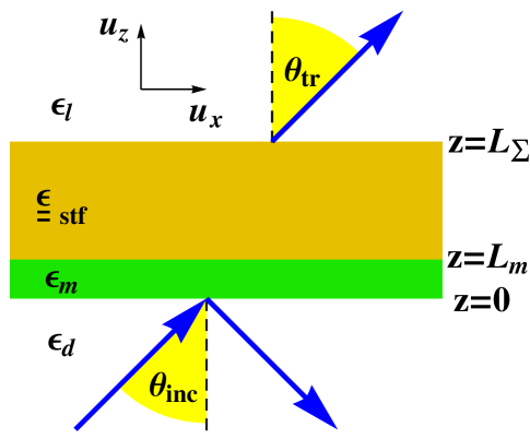
As a realistic setup for launching SPP waves along the planar interface of a metal film and a CSTF, we consider the modification [40] to the standard Kretschmann configuration [41] illustrated schematically in Fig. 1. The regions and are assumed to be occupied by homogeneous, isotropic, nondissipative, dielectric materials with relative permittivity scalars and , respectively. A CSTF — infiltrated by a fluid of refractive index — occupies the laminar region , while the laminar region is occupied by a metal with relative permittivity .
2.1 Constitutive and morphological parameters of CSTF
A CSTF comprises an array of parallel helical nanowires [18]. It may been grown on a planar substrate, lying parallel to the plane say, by the deposition of an evaporated bulk material. On rotating the substrate about the axis at a uniform angular speed throughout the deposition process, helical nanowires grow along the direction, with the rise angle of each nanowire, relative to the plane, being denoted by . The deposited material is assumed to be an isotropic dielectric material of refractive index . Significantly, can be different from the refractive index of the bulk material that was evaporated [42, 43, 44].
The helical shape of each nanowire of a CSTF can be viewed as a string of highly elongated ellipsoidal inclusions, wound end-to-end around the axis [45, 46]. The shape dyadic
| (1) |
wherein the normal, tangential, and binormal basis vectors are given as
| (2) |
prescribes the surface of each ellipsoidal inclusion. An aciculate shape is imposed on the inclusions by selecting the shape parameters and . Increasing beyond 10 does not give rise to significant effects for slender inclusions [46]. Accordingly, for the numerical results which follow in §3, was chosen. The proportion of a CSTF’s total volume occupied by helical nanowires is ; equivalently, the volume fraction of the CSTF not occupied by nanowires is .
The relative permittivity dyadic
| (3) |
characterizes the CSTF at length scales much greater than the nanoscale. Herein the handedness parameter for a structurally right (left)-handed CSTF; the rotation dyadics
| (4) |
and is the structural period. We take to be a positive–valued integer; i.e., the CSTF contains a whole number of structural periods. The reference relative permittivity dyadic has the orthorhombic form
| (5) |
where for a CSTF in which the void regions are vacuous (i.e., an uninfiltrated CSTF) and for a CSTF in which the void regions are filled with a fluid of refractive index .
In principle, the relative permittivity parameters of an uninfiltrated CSTF are measurable. However, in the absence of suitable measured data for CSTFs, recent numerical studies have used values of measured for related CTFs. The nanoscale model parameters — which are not readily determined by experimental means — can be determined from a knowledge of by applying the inverse Bruggeman homogenization formalism [47]. Once have been found, they can be combined with in order to determine the relative permittivity parameters for the infiltrated CSTF, by applying the Bruggeman homogenization formalism in its usual forward sense [26, 46].
2.2 Boundary-value problem
The essence of the sensing mechanism in the modified Kretschmann configuration is described by the following boundary-value problem [40]. An arbitrarily polarized plane wave is launched in the half-space towards the metal layer. We suppose that its wavevector lies in the plane, making an angle relative to the axis. This incident plane-wave gives rise to a reflected plane wave in the half-space and a transmitted plane wave in the half-space . Thus, the total electric field phasor in the half-space may be expressed as
| (6) | |||||
while that in the half-space may be expressed as
| (7) |
wherein , and the angle of transmission satisfies the law of Ibn Sahl [18] as follows:
| (8) |
By solving the related boundary-value problem, the complex–valued reflection and transmission amplitudes, namely , , and , are related to the corresponding amplitudes and of the and polarized components of the incident plane wave. This standard procedure yields the algebraic relation [29]
| (9) |
wherein the 44 matrixes
| (10) |
| (11) |
The transfer matrix of one structural period of the CSTF and its evaluation are comprehensively described elsewhere [18, 29]. From (9), we may write
| (12) |
thereby introducing the reflection coefficients and transmission coefficients . The square magnitude of a reflection coefficient delivers the corresponding reflectance; i.e.,
| (13) |
The four transmittances are defined as follows:
| (14) |
The absorbances for and polarization states of the incident plane wave, namely
| (15) |
play a key role in identifying SPP waves. A sharp high peak in the graph of absorbance versus , arising at say, is a signature of SPP excitation at the interface provided that
-
(i)
is insensitive to changes in the CSTF’s thickness and
- (ii)
3 Numerical results and discussion
The helical morphology of a CSTF is nanoengineered by obliquely directing a collimated vapor flux in high vacuum towards a planar substrate that rotates about a fixed axis at a constant rate [18]. The angle between the average direction of the vapor flux and the substrate plane determines the dielectric properties of the CSTF. In view of the absence of suitable experimental data for CSTFs, for our numerical studies we chose the relative permittivity parameters
| (17) |
with
| (18) |
which were determined by experimental measurements at a free–space wavelength of 633 nm on a CTF made from patinal titanium oxide [50, 51]. Values for the corresponding nanoscale model parameters , as computed using the inverse Bruggeman homogenization formalism [47], are provided in Table 1 for the vapor flux angles , , and . Furthermore, we set and normalized the CSTF’s structural half-period relative to nm. The metal was taken to be aluminum with relative permittivity at nm, and the thickness of the metal film nm. The relative permittivity which is typical of zinc selenide.
The parameter values chosen are consistent with those chosen for an earlier study involving an uninfiltrated CSTF () [29], thereby allowing direct comparisons to be made. Extrapolating from this earlier study, we expect there to be up to five modes of SPP-wave propagation at the planar metal/CSTF interface, depending upon the value of the ratio . The manifestation of these SPP modes in graphs of absorbance versus angle of incidence was tracked from the earlier study [29] to the present study by continuously varying the refractive index . Further confirmation of the SPP status of the absorbance peaks was provided by checking that the corresponding eigenvalues of the transfer matrix have non-zero imaginary parts, per [48, 49].
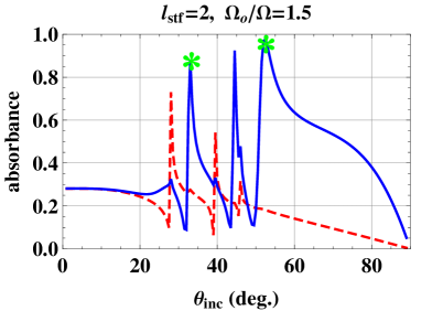
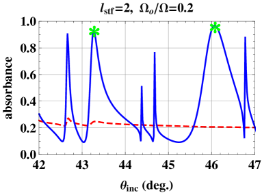
We begin our presentation of numerical results with the graphs of absorbance for incident light of and polarization states versus in Fig. 2. Here , , and . The peaks at and represent the SPP modes 1 and 2, respectively (in the terminology of Polo and Lakhtakia [29]).
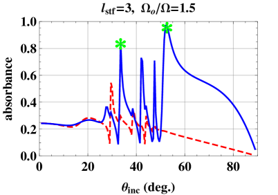
The non-SPP peaks and the peaks which appear in Fig. 2 indicate waveguide modes [52] which must depend upon the thickness of the CSTF. To demonstrate this, in Fig. 3 the graphs of Fig. 2 are reproduced except that here . We see that the peaks corresponding to the SPP modes 1 and 2 remain fixed in position but the other and peaks have moved relative to their positions in Fig. 2.
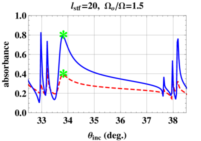
There are no peaks corresponding to the two SPP peaks in Figs. 2 and 3. However, by considerably increasing the thickness of the CSTF, evidence of a SPP emerges. Fig. 4 is as Figs. 2 and 3 except that here and we focus on the angle of incidence range . We see that a peak has emerged at ; i.e., at the same position as the mode 2 SPP peak. A corresponding peak was reported for the case of an uninfiltrated CSTF [29]. The large thickness needed is due to the slow decay rate of the electromagnetic fields in the thickness direction [30].
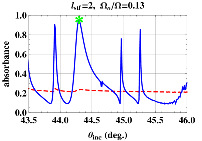
The SPP modes 3–5 only exist only for values of lower than that considered in Figs. 2–4. In Fig. 5 the peaks corresponding to SPP modes 3 and 4 can be seen at and , respectively, for in the plot of absorbance versus angle of incidence. Also, the peak corresponding to SPP mode 5 can be seen at for in the plot of absorbance versus in Fig. 6. As in Figs. 2–4, the non–SPP peaks which appear in Figs. 5 and 6 represent waveguide modes, as has been confirmed by additional computations (not presented here) for different CSTF thicknesses.
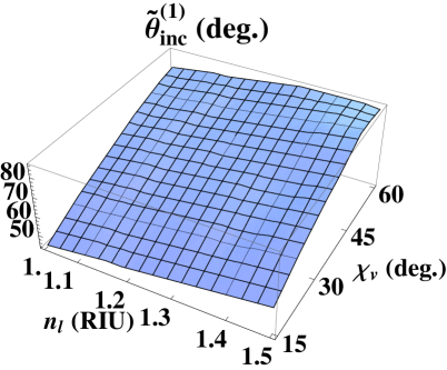
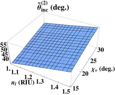
The values of at which the SPP peaks appear in the graphs of absorbance are sensitive to both the refractive index of the fluid infiltrating the CSTF and the vapor incidence angle . The value of at which the absorbance peak arises for the SPP mode — let us denote this value as at a specific value of — is plotted versus and for , and versus and for , in Fig. 7. Here and . It may be observed that uniformly increases as increases and as increases. A similar trend is exhibited by . The corresponding plots for , and (not provided here) also follow the same general trends as those displayed in Fig. 7. We note that for and , the SPP mode 1 vanishes as approaches . Furthermore, as compared to the SPP mode 1, the SPP mode 2 exists only for a smaller -range. Indeed, as compared to the SPP mode 2, the SPP modes 3–5 exist for even smaller -ranges. The general trends displayed in Fig. 7 are the same as those reported for an analogous study based on an infiltrated CTF [38].
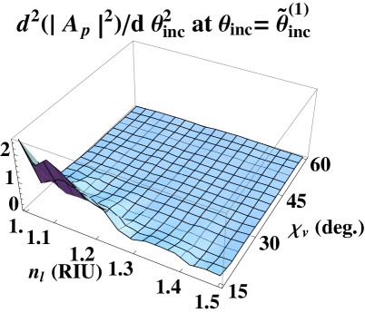
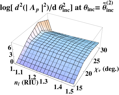
For optical-sensing applications, a feature of practical significance is the shape of the SPP peaks in graphs of absorbance versus angle of incidence. For the SPP mode 1 represented in Fig. 7, the sharpness of this peak, as gauged by the second derivative evaluated at , is plotted in Fig. 8 against and . The sharpness of the selected peak decreases as increases from 1.0 and as increases from . The most dramatic changes in sharpness occur at when both and have low values. The trends in Fig. 8 for the SPP mode 1 are qualitatively similar to those reported for an analogous study based on an infiltrated CTF [38], over the range . Also provided in Fig. 8 is the corresponding plot of evaluated at . The peak for the SPP mode 2 is clearly much sharper than the peak for the SPP mode 1, across the entire range of values and values considered. Similarly, the peaks for the SPP modes 3–5 were found to be much sharper than the peak for the SPP mode 1.
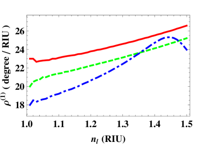
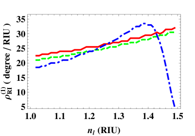
Let us now further consider the sensitivity of the SPP peaks in the graphs of absorbance versus angle of incidence to both and . As in Figs. 7 and 8, we fix and . The figure of merit (in degree/RIU444RIU = refractive-index unit)
| (19) |
wherein is expressed as a function of , is a measure of sensitivity for the SPP mode . Graphs of versus are provided in Fig. 9 for . Also, is plotted versus for . Generally, is most sensitive to changes in when is small and is large, in keeping with an analogous study based on an infiltrated CTF [38]. A similar trend is followed by —and by , , which are not represented in Fig. 9. Furthermore, the magnitudes of for all are broadly similar. There are quantitative differences between the present CSTF scenario for the SPP mode 1 and the analogous CTF scenario for the sole SPP mode: the sensitivities for are greater for the latter scenario whereas the sensitivities for are greater for the former scenario.
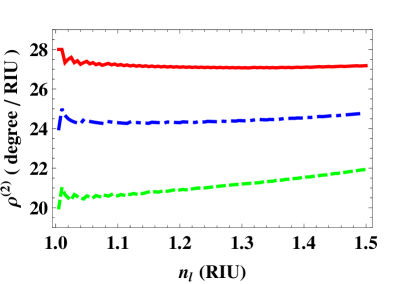
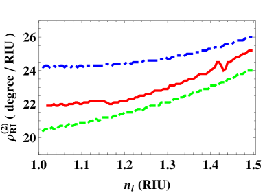
An alternative measure of sensitivity is provided by the refractive-index sensitivity [33]
| (20) |
also expressed in degree/RIU. While is the analog of the voltage-current ratio in electrical circuitry, is the analog of the dynamic resistance . In Fig. 10, and are plotted against with all CSTF parameters being the same as those used for Fig. 9. Generally, is dynamically most sensitive to changes in when is large. This general trend with respect to for the SPP mode 1 is the opposite to that reported for an analogous study based on an infiltrated CTF [38]. The influence of on the dynamic sensitivity is less clear cut, as it depends upon the value of and which SPP mode is being considered. The magnitudes of and —and , and not represented in Fig. 10—are broadly similar.
4 Closing remarks
Numerical simulations with an empirical model have revealed that the excitation of mutliple SPP waves guided by the planar interface of a metal film and a CSTF is acutely sensitive to both the refractive index of a fluid infiltrating the CSTF and the morphology of the CSTF itself. Thus, the potential for a SPP–based CSTF optical sensor has been demonstrated. The SPP sensitivities reported here are, by and large, similar to those reported for an analogous study based on an infiltrated CTF [38]. However, in contrast to just one modality—angular shift of just one SPP mode—offered by CTFs, CSTFs offer multiple modalities. These are of two types: (i) angular shifts of more than SPP mode, and (ii) spectral shift of the circular Bragg phenomenon [26]. More than one of these modalities can be implemented simultaneously.
Acknowledgments: TGM is supported by a Royal Academy of Engineering/Leverhulme Trust Senior Research Fellowship. AL thanks Bernhard Michel (Simuloptics GmbH, Schwabach, Germany) for a discussion on Reusch’s 1869 paper and the Binder Endowment at Penn State for partial financial support of his research activities.
References
- [1] P. J. Collings, Liquid Crystals: Nature’s Delicate Phase of Matter. Princeton, NJ, USA: Princeton University Press, 1990.
- [2] A. S. Sonin, “What are liquid crystals? (On the 100th anniversary of the discovery),” J. Struct. Chem., vol. 32, pp. 111–129, 1991.
- [3] T. J. Sluckin, D. A. Dunmur, and H. Stegemeyer, Crystals That Flow: Classic Papers from the History of Liquid Crystals. London, United Kingdom: Taylor & Francis, 2004.
- [4] F. Reinitzer, “Beiträge zur Kenntiss des Cholesterins,” Monat. Chem. (Wien), vol. 9, pp. 421–441 (1888). See Sluckin et al. [3] for an English translation.
- [5] H. Kelker, “Survey of the early history of liquid crystals,” Mol. Cryst. Liq. Cryst., vol. 165, pp. 1–43, 1988.
- [6] M. G. Friedel, “Les états mésomorphes de la matière,” Ann. Phys. (Paris), vol. 18, pp. 273–474 (1922). See Sluckin et al. [3] for an English translation of significant excerpts.
- [7] C. Darwin, On the Movements and Habits of Climbing Plants. London, UK: Longman, Green, 1865.
- [8] K. S. Gould and D. W. Lee, “Physical and ultrastructural basis of blue leaf iridescence in four Malaysian understory plants,” Am. J. Botany, vol. 83, pp. 45–50 (1996).
- [9] J. Fergason, “Cholesteric structure—I. Optical properties,” Mol. Cryst. vol. 1, pp. 293–307 (1966).
- [10] S. D. Jacobs (ed.), Selected Papers on Liquid Crystals for Optics. Bellingham, WA, USA: SPIE Press, 1992.
- [11] E. Reusch, “Untersuchung ber Glimmercombinationen,” Ann. Phys. Chem. Lpz., vol. 138, pp. 628–639, 1869.
- [12] G. Joly and N. Isaert, Quelques champs électromagnétiques dans les piles de Reusch IV — Domaines multiples de réflexion sélective,” J. Opt. (Paris), vol. 17, pp. 211–221, 1986.
- [13] I. J. Hodgkinson, A. Lakhtakia, Q. H. Wu, L. De Silva, and M. W. McCall, “Ambichiral, equichiral and finely chiral layered structures,” Opt. Commun., vol. 239, pp. 353–358, 2004.
- [14] N. O. Young and J. Kowal, “Optically active fluorite films,” Nature, vol. 183, pp. 104–105, 1959.
- [15] E. F. Dawson and N. O. Young, “Helical Kerr cell,” J. Opt. Soc. Am., vol. 50, pp. 170–171, 1960.
- [16] A. Lakhtakia and R. Messier, “The key to a thin film HBM: the Motohiro-Taga interface,” Proceedings of Chiral ’94: 3rd International Workshop on Chiral, Bi-isotropic and Bi-anisotropic Media (F. Mariotte and J.-P. Parneix, eds), Périgueux, France (May 18-20, 1994), pp. 125–130.
- [17] A. Lakhtakia, R. Messier, M.J. Brett, and K. Robbie, “Sculptured thin films (STFs) for optical, chemical and biological applications,” Innovat. Mater. Res. vol. 1, pp. 165–176, 1996.
- [18] A. Lakhtakia and R. Messier, Sculptured Thin Films: Nanoengineered Morphology and Optics. Bellingham, WA, USA: SPIE Press, 2005.
- [19] A. Lakhtakia, M. C. Demirel, M. W. Horn, and J. Xu. “Six emerging directions in sculptured-thin-film research,” Adv. Solid State Phys., vol. 46, pp. 295–307, 2008.
- [20] R. Walser, “Metamaterials: An introduction,” in W. S. Weiglhofer and A. Lakhtakia, editors, Introduction to Complex Mediums for Optics and Electromagnetics, Bellingham, WA, USA: SPIE Press, 2003, pp. 295–316.
- [21] A. Lakhtakia and T. G. Mackay, “Meet the metamaterials,” OSA Opt. Photon. News, vol. 18, no. 1, pp. 32–37, 2007.
- [22] Q. Wu, I. J. Hodgkinson, and A. Lakhtakia, “Circular polarization filters made of chiral sculptured thin films: experimental and simulation results,” Opt. Eng., vol. 39, pp. 1863–1868, 2000.
- [23] F. Chiadini and A. Lakhtakia, “Design of wideband circular-polarization filters made of chiral sculptured thin films,” Microwave Opt. Technol. Lett., vol. 42, pp. 135–138, 2004.
- [24] Y. J. Park, K. M. A. Sobahan, and C. K. Hwangbo, “Wideband circular polarization reflector fabricated by glancing angle deposition,” Opt. Exp., vol. 16, pp. 5186–5192, 2008.
- [25] I. J. Hodgkinson, Q. H. Wu, K. E. Thorn, A. Lakhtakia, and M. W. McCall, “Spacerless circular-polarization spectral-hole filters using chiral sculptured thin films: theory and experiment,” Opt. Commun., vol. 184, pp. 57–66, 2000.
- [26] T. G. Mackay and A. Lakhtakia, “Empirical model of optical sensing via spectral shift of circular Bragg phenomenon,” IEEE Photonics Journal, vol. 2, pp. 92–101, 2010.
- [27] A. Lakhtakia, M. W. McCall, J. A. Sherwin, Q. H. Wu, and I. J. Hodgkinson, “Sculptured-thin-film spectral holes for optical sensing of fluids,” Opt. Commun., vol. 194, pp. 33–46, 2001.
- [28] S. M. Pursel and M. W. Horn, “Prospects for nanowire sculptured-thin-film devices,” J. Vac. Sci. Technol. B, vol. 25, pp. 2611–2615, 2007.
- [29] J. A. Polo, Jr and A. Lakhtakia, “On the surface plasmon polariton wave at the planar interface of a metal and chiral sculptured thin film,” Proc. R. Soc. A, vol. 465, pp. 87–107, 2009.
- [30] J. A. Polo, Jr. and A. Lakhtakia, “Energy flux in a surface-plasmon-polariton wave bound to the planar interface of a metal and a structurally chiral material,” J. Opt. Soc. Am. A, vol. 26, pp. 1696–1703, 2009.
- [31] Devender, D. P. Pulsifer, and A. Lakhtakia, “Multiple surface plasmon polariton waves,” Electron. Lett., vol. 45, pp. 1137–1138, 2009.
- [32] D. Felbacq, “Plasmons go quantum,” J. Nanophoton., vol. 2, 020302, 2008.
- [33] J. Homola, “Present and future of surface plasmon resonance biosensors,” Anal. Bioanal. Chem., vol. 377, pp. 528–539, 2003.
- [34] X. Fan, I. M. White, S. I. Shopova, H. Zhu, J. D. Suter, and Y. Sun, “Sensitive optical biosensors for unlabeled targets: A review,” Anal. Chim. Acta, vol. 620, pp. 8–26, 2008.
- [35] J. Homola, “Surface plasmon resonance sensors for detection of chemical and biological species,” Chem. Rev., vol. 108, pp. 462–493, 2008.
- [36] I. Abdulhalim, M. Zourob, and A. Lakhtakia, “Surface plasmon resonance for biosensing: A mini-review,” Electromagnetics, vol. 28, pp. 214–242, 2008.
- [37] S. Scarano, M. Mascini, A. P. F. Turner, and M. Minunni, “Surface plasmon resonance imaging for affinity–based biosensors,” Biosens. Bioelectron., vol. 25, pp. 957–966, 2010.
- [38] T. G. Mackay and A. Lakhtakia, “Modeling columnar thin films as platforms for surface–plasmonic–polaritonic optical sensing,” Photon. Nanostruct. Fundam. Appl. (at press). doi:10.1016/j.photonics.2010.02.003
- [39] J. A. Polo Jr. and A. Lakhtakia, “Surface electromagnetic waves: A review,” Laser Photon. Rev. (at press). doi:10.1002/lpor.200900050
- [40] A. Lakhtakia, “Surface-plasmon wave at the planar interface of a metal film and a structurally chiral medium,” Opt. Commun., vol. 279, pp. 291–297, 2007.
- [41] E. Kretschmann and H. Raether, “Radiative decay of nonradiative surface plasmons excited by light,” Z. Naturforsch. A, vol. 23, pp. 2135–2136, 1968.
- [42] R. Messier, T. Takamori, and R. Roy, “Structure-composition variation in rf-sputtered films of Ge caused by process parameter changes,” J. Vac. Sci. Technol., vol. 13, pp. 1060-1065, 1976.
- [43] J. R. Blanco, P. J. McMarr, J. E. Yehoda, K. Vedam, and R. Messier, “Density of amorphous germanium films by spectroscopic ellipsometry,” J. Vac. Sci. Technol. A, vol. 4, pp. 577-582, 1986.
- [44] F. Walbel, E. Ritter, and R. Linsbod, “Properties of TiO films prepared by electron-beam evaporation of titanium and titanium suboxides,” Appl. Opt., vol. 42, pp. 4590-4593, 2003.
- [45] J. A. Sherwin, A. Lakhtakia, and I. J. Hodgkinson, “On calibration of a nominal structure-property relationship model for chiral sculptured thin films by axial transmittance measurements,” Opt. Commun., vol. 209, pp. 369-375, 2002.
- [46] A. Lakhtakia, “Enhancement of optical activity of chiral sculptured thin films by suitable infiltration of void regions,” Optik, vol. 112, pp. 145-148, 2001. Erratum: vol. 112, p. 544, 2001.
- [47] T. G. Mackay and A. Lakhtakia, “Determination of constitutive and morphological parameters of columnar thin films by inverse homogenization,” J. Nanophoton., vol. 4, 041535, 2010.
- [48] M. A. Motyka and A. Lakhtakia, “Multiple trains of same-color surface plasmon-polaritons guided by the planar interface of a metal and a sculptured nematic thin film. Part II: Arbitrary incidence,” J. Nanophoton., vol. 3, 033502, 2009.
- [49] M. Faryad, J. A. Polo Jr., and A. Lakhtakia, “Multiple trains of same-color surface plasmon-polaritons guided by the planar interface of a metal and a sculptured nematic thin film. Part III: Canonical problem,” J. Nanophoton., vol. 4, 043505, 2010.
- [50] I. Hodgkinson, Q. h. Wu, and J. Hazel, “Empirical equations for the principal refractive indices and column angle of obliquely deposited films of tantalum oxide, titanium oxide, and zirconium oxide,” Appl. Opt., vol. 37, pp. 2653–2659, 1998.
- [51] F. Chiadini and A. Lakhtakia, “Extension of Hodgkinson’s model for optical characterization of columnar thin films,” Microw. Opt. Technol. Lett., vol. 42, pp. 72-73, 2004.
- [52] M. A. Motyka and A. Lakhtakia, “Multiple trains of same-color surface plasmon-polaritons guided by the planar interface of a metal and a sculptured nematic thin film,” J. Nanophoton., vol. 2, 021910, 2008.
| 2.2793 | 0.3614 | 3.2510 | |
| 1.8381 | 0.5039 | 3.0517 | |
| 1.4054 | 0.6956 | 2.9105 |
