Electronic implementations of Interaction-Free Measurements
Abstract
Three different implementations of interaction-free measurements (IFMs) in solid-state nanodevices are discussed. The first one is based on a series of concatenated Mach-Zehnder interferometers, in analogy to optical-IFM setups. The second one consists of a single interferometer and concatenation is achieved in the time domain making use of a quantized electron emitter. The third implementation consists of an asymmetric Aharonov-Bohm ring. For all three cases we show that the presence of a dephasing source acting on one arm of the interferometer can be detected without degrading the coherence of the measured current. Electronic implementations of IFMs in nanoelectronics may play a fundamental role as very accurate and noninvasive measuring schemes for quantum devices.
pacs:
03.65.Ta, 03.67.Lx, 42.50.Dv, 42.50.Pq,I Introduction
Interaction-free measurements (IFMs) were first introduced by Elitzur and Vaidman ElitzurVaidman , who showed that the laws of quantum mechanics allow to reveal the presence of an object without disturbing it. The original proposal exploited the coherent splitting and the subsequent recombination of the wave-function of a photon entering a Mach-Zehnder (MZ) interferometer. The disturbance induced by the object placed in one of the two arms of the interferometer (an absorber in the original proposal) manifests itself in the properties of the outgoing photon flux. Upon suitable setting of the interferometer parameters it was shown that even without absorption taking place its mere possibility does modify the state of the particle emerging from the interferometer. As a result an external observer will be able to gather information about the presence or absence of the absorber, without the photon being actually absorbed. The maximal success probability was bound to be 50% in the original proposal. A way to improve the efficiency of the scheme was put forward by P. Kwiat et al. KwiatPRL95 , who suggested to use coherently repeated interrogations. In their scheme a photon was repeatedly sent into a MZ interferometer, with an absorber placed in one of the two arms. By properly tuning the MZ phase it was shown that it is possible to enhance the efficiency of the setup arbitrarily close to 1. Such a scheme can be thought as an application of a discrete form of the quantum Zeno effectZENO since every step can be considered as a measurement accompanied by state reduction.
IFMs were experimentally realized using single-photon sources KwiatPRL95 ; TsegayePRA98 ; WhitePRA98 ; vanVoorthuysen96 and in neutron interferometry HafnerPhysLettA97 . The enhanced efficiency of concatenated MZ interferometers schemes was tested in Ref. [KwiatPRL99, ] with a demonstrated improvement up to 73%. Its application was extended to the case of semitransparent objects with classical light JangPRA99 ; PAVICIC ; INOUE ; GiovannettiOptExp06 . An important consequence of these works is that IFM can be interpreted in terms of deterioration of a resonance condition PAVICIC which does not necessarily need a quantum description (“classical” optical coherence is sufficient), at least for these optical realizations.
The implementation of IFM in electronic devices deserves in our opinion a careful scrutiny since it constitutes an ideal test-bed for the study of quantum-control and quantum-mechanics phenomena in mesoscopic systems. It is worth noting that, differently from the optical case, for electronic systems there is no corresponding classical model to realize an IFM. In recent years advances in device fabrication opened the way to the observation of interference phenomena in electronic-transport experiments, suggesting important opportunities for a variety of applications. The achievements obtained in the context of two-dimensional electron gases in the integer quantum Hall effect regime GOERBIG are of particular interest for what follows. Here, various experimental realizations of the MZ JiNature03 ; NederPRL06 ; LitvinPRB07 ; RoulleauPRB07 ; NederNatPh07 and Hanbury-Brown-Twiss interferometers SamuelssonPRL04 ; NederNatur07 were successfully implemented. In addition, quantized electron emitters were recently realized Moskalets08 ; Splettstoesser08 ; Gabelli06 ; Feve07 . The possibility to extend IFM to electronic systems seems therefore now at reach, paving the way to the development of novel non-invasive measurement schemes in mesoscopic systems, with possible important implications for quantum information processing.
A first application of IFM strategies to electronic systems was proposed in Ref. [PARA, ] to detect the presence of a current pulse in a circuit by monitoring the state of a superconducting qubit coupled to the circuit, without any energy exchange between the two. Subsequently, in the very same spirit of the original works ElitzurVaidman ; KwiatPRL95 , it was shown how to employ IFM to detect with unitary efficiency a source of noise acting on one arm of an Aharonov-Bohm (AB) chiral ring without affecting the transmitted and reflected currents NOI09 . In view of its (unavoidable) presence in nanoelectronics, the proposal focused on the detection of external random fluctuating electric or magnetic fields, which represents the most common source of noise in nanoscale quantum devices MarquardtPRB02 ; MarquardtPRB03 ; MarquardtPRL04 . Therefore, in Ref. [NOI09, ] a classical fluctuating electrical field that randomizes the phase of the electron traveling through it played the role of the absorber in optical schemes ElitzurVaidman ; KwiatPRL95 ; TsegayePRA98 ; WhitePRA98 ; vanVoorthuysen96 ; HafnerPhysLettA97 ; KwiatPRL99 ; JangPRA99 ; PAVICIC ; INOUE ; GiovannettiOptExp06 . The resulting apparatus operates as a sort of quantum fuse which opens or closes a contact depending on the presence or on the absence of the dephasing source. The results presented in Ref. [NOI09, ] show that the mechanism underlying the IFM does not depend, to a large extent, on the type of disturbance which is induced in the interferometer.
In the present paper we extend our previous work NOI09 on the electronic version of the IFM in several ways. First of all we introduce two alternative IFM implementations based on the integer quantum Hall effect. The first scheme closely resembles the optical setup of Ref. [KwiatPRL99, ] and uses a recent proposal GiovannettiPRB08 for realizing concatenated MZ interferometers. The second scheme instead is based on the standard quantum Hall interferometric architecture JiNature03 ; NederPRL06 ; LitvinPRB07 ; RoulleauPRB07 ; NederNatPh07 ; SamuelssonPRL04 ; NederNatur07 and assumes the presence of a quantized electron emitter Gabelli06 ; Feve07 ; Moskalets08 ; Splettstoesser08 . As in Ref. [NOI09, ], both setups are shown to be capable of detecting the presence of a localized dephasing source without affecting the coherence of the probing signals. Finally we review the AB-ring implementation of Ref. [NOI09, ] and provide a detailed characterization of the scheme.
The paper is organized as follows. In Sec. II we present a noise-sensitive coherent electron detector, based on the concatenation of several MZ interferometers. We show that we can detect the presence of a dephasing source affecting propagation in one of the interfering electronic paths by measuring the output currents. We then study the coherence of the outgoing signal by computing the fraction of coherent signal and show that an IFM measurement of the dephasing source is achievable. In Sec. II.3 we embed the device described in Sec. II in a larger Mach-Zehnder interferometer and study the visibility of the output currents, showing how the coherence of the outgoing signal can be experimentally addressed. In Sec. III we propose an implementation of IFM based on a single Mach-Zehnder interferometer that makes use of a quantized electron source and concatenation in the time domain. In Sec. IV we present a double ring structure in which a small chiral AB ring is embedded in one arm of a larger AB ring. We show that the current which flows through the whole device is a measure of the coherent character of the detection.
II Coherent detection of noise with IFMs
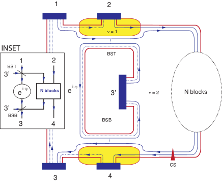
A straightforward implementation of IFM along the lines developed originally in optics can be realized exploiting the edge-channel interferometric architecture of Ref. [GiovannettiPRB08, ] based on the integer quantum Hall effect at filling factor . The feature of this architecture which is particularly relevant for our purposes is that it allows for successive concatenations of different interferometers. In this scheme, beam splitters (BSs) are realized by introducing a sharp potential barrier which mixes the two edges. Populating initially only one channel, at the output of a BS we find electrons in a superposition state. Additional phase shifters (PSs) can be easily realized by spatially separating the two channels with the used of a top gate that can locally change the filling factor to : only one channel can traverse the region at and the other is guided along its edges. This is schematically shown in Fig. 1, where a phase difference is introduced between the channels by changing the path of the incoming channel.
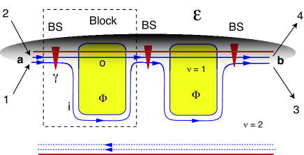
Based on this approach we can build an apparatus which implements an IFM scheme Along the lines of the optical setup of Ref. [KwiatPRL99, ]. The proposed device, illustrated in Fig. 1, consists in a sequence of interferometric elements, in which output edges emerging from the -th interferometer are directly fed into the input of the -th one. As we shall see, the apparatus allows one to detect the presence of a fluctuating electromagnetic field affecting the upper region of the Hall bar (depicted as a shaded area in Fig. 1), without any coherence loss of the transmitted currents. This is obtained thanks to the action of the top gates of the setup which divert the path of the (inner) channel inside the Hall bar (where the fluctuating field is supposed to be absent), and thanks to the coherent mixing between the channel and the (outer) channel induced by the BSs. If no dephasing is present in the upper region of the bar, then the electron coherently propagates towards the next step, that is nominally equal to the previous one. By properly tuning the degree of admixture of the channel populations, it is possible to gradually transfer the electron from the channel to the channel at the end of a chain of interferometers. The situation changes completely when the dephasing field is present in the shaded region of Fig. 1. Indeed, as a result of a random phase shift, the part of the wave-function that propagates in the channel does not coherently add to the one propagating in the channel. Consequently the gradual transfer of electronic amplitude from to does not take place. At the same time the electron that propagates into the channel not exposed to the fluctuating field preserves its coherence. The presence or absence of noise is revealed by the electron emerging from lead 3 or 4, respectively and, as we shall clarify in the following, the setup does preserve the coherence of the emerging electronic signal.
II.1 Detection of a dephasing noise source
Electron propagation is described in the Landauer-Büttiker formalism of quantum transport Buttiker85 ; Buttiker88 . The scattering matrix that describes transport in each block can be written as:
| (1) |
where parametrizes the degree of edge-channel mixing introduced by BS, and is the phase shift between the two edge channels. The presence of a dephasing source is described by a random phase shift . By using this scattering matrix it is possible to relate electrons exiting the chain of blocks to the incoming ones at the beginning of the chain:
| (2) |
with being the Fermionic annihilation operator describing incoming electrons in leads 1 and 2 (connected to channels and , respectively), and the Fermionic annihilation operator describing outgoing electrons (leads 3 and 4). Contact 1 is biased at a chemical potential , reservoirs 2, 3, and 4 are kept at reference potential. Setting the temperature to zero, the current in contact is
| (3) |
while the current in contact 4 is
| (4) |
with . Here we do not take into consideration the electron-spin degree of freedom.
The effect of the fluctuating field can be taken into account by averaging the phases over a generic distribution of width and zero mean. For simplicity we assume a uniform distribution. The outgoing currents depend now entirely on the degree of mixing of edge states in the BS and on the phase shift . The average current in contact 3 (4) is given by
| (5) |
with . We define the two-component vectors , , that allow us to express
| (6) | |||||
| (7) |
Introducing a representation of matrices in terms of Pauli operators, concisely written through the Pauli vector , with , we can write , with . This allows us to calculate the average over phases as a matrix product. By defining matrix
| (8) |
we can write the zero-temperature average current in output 3 (4) after blocks as
| (9) |
We point out that, due to the unitarity of , defined in Eq. 8 preserves the trace. One can reduce the dimensionality of the problem and work with the Bloch representation of density matrices.
The behavior of the output currents in the limit of large is obtained by studying the eigenvalues of the matrix . Choosing the working point , assumes a diagonal block form that allows a direct solution: , with and given by Eqs. 34,35 in Appendix B. The currents in terminal 3 (4) can be then written as
| (10) |
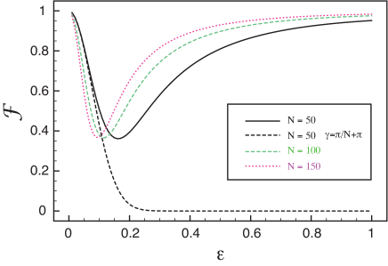
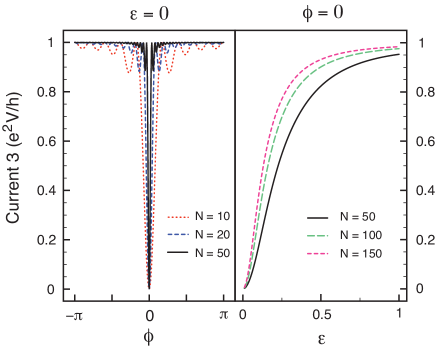
Figure 2 (left panel) shows the current in terminal 3 versus the phase shift for the case of no dephasing (). We can see that for large , is approximately for almost all values of , and that only at it drops very rapidly to zero. For such value the outgoing currents are indeed and independently from (increasing further shrinks the dip at ). This corresponds to having a very narrow resonance at the working point where interference gives rise to a gradual transfer of the electron wave-function to the channel and all the current emerges from contact 4. Such a resonance is very sensitive to small deviations of the phase from the working point and imply a large variation of the current response.
In the case of strong dephasing () the current is instead given by
| (11) |
If the asymmetry of the BSs is properly tuned at the value , the output currents are , so that, in the limit of large , one finds that and . The behavior of the current in contact 3 versus the dephasing strength is shown in Fig. 2, right panel. It is evident that the presence of a strong dephasing source changes the interference response, so that for all electrons exit the device from terminal 3, whereas in the coherent case they would exit from terminal 4. Thus, in this respect the system behaves like a “which-path” electronic interferometer ALE . Interestingly we note that Eq. (11) predicts that, for even , the same behavior can be observed also in the highly asymmetric case when the electronic amplitude is diverted to the noisy channel , i.e. . In the next section we shall see however that, differently to the case , this last regime does not correspond to a true IFM effect, since the coherence of the transmitted signals is totally washed out.
II.2 Coherence of the outgoing signal
A key feature of the IFM detection of noise is that coherence of the output be preserved and this can open the way to novel applications in quantum-coherent electronics. Depending on whether the electron is mostly injected into the secure channel by setting or into the channel exposed to dephasing, by setting , the coherence of the outgoing signal can be asymptotically preserved or totally lost.
An effective way to quantify the coherence of the outgoing signal can be obtained by defining the fraction of coherent signal as
| (12) |
where we have set and so that () is the averaged transmission amplitude to contact 3 (4). takes values between 0 (complete loss of coherence) and 1 (coherence fully preserved, since in this case ). The two quantities and measure the coherence of the transmitted electrons into contacts 3 and 4, respectively, since they are proportional to the interference terms of such electrons with a reference, coherent, signal (a thorough discussion is given in Sec. II.3). In Fig. 3 we plot for different choices of and . For , the fraction of coherent signal initially decreases as a result of the disturbance induced by the fluctuating field (degradation of coherence). For large values of , however, the dephasing of the tiny portion of the wavefunction pertinent to the channel prevents the occurrence of destructive interference. As a result full, coherent transmission through the lower arm of the setup is established, yielding and thus indicating that an IFM is taking place in the setup. This can be understood as due to the quantum Zeno effect ZENO associated with repetitive measurements that try to determine whether or not the electron is “passing” through the upper arm of the interferometer NOI09 . For , the outcome of such a measurement will be negative with a very high probability (i. e. the electron is found in the lower arm) preserving coherence. An interplay between these two regimes occurs for intermediate values of giving rise to a minimum in which sharpens for higher (see Fig. 3). This scenario changes completely for . Here electrons are mostly injected into the channel. For small values of the situation is analogous to the case , the behavior of being actually the same: the noise source induces a partial suppression of the destructive interference yielding a consequent degradation of coherence. As evident from Fig. 3 however, in this case large values of yields a drop of to zero indicating that no IFM is taking place here. This originates from the fact that the complete suppression of the destructive interference is accompanied by a likewise complete loss of coherence due to the strong dephasing experienced by the electron.
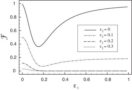
So far we have considered an ideal situation in which dephasing takes place only in the channel. Figure 4 shows the behavior of versus the strength of the dephasing field acting on channel , when a fluctuating field of strength affects propagation in the channel. We see that a strong response corresponds to a slight increase of , with the coherence of the outgoing signal being significantly degraded.
II.3 Detection of the coherent signal
In this section we show that the fraction of coherent signal defined in Eq. 12 can actually be measured by embedding the concatenated blocks in a Mach-Zehnder interferometer, as schematically illustrated in Fig. 5. A voltage is applied to contact 1, while all other contacts are at reference potential. A beam splitter (BST in Fig. 5) splits the current injected by contact 1 so that the transmitted portion enters the -block system from channel , while the reflected one follows a path whose length (and phase ) can be arbitrarily adjusted. The current exiting the -block system via channel is then mixed with the signal of known phase at beam splitter BSB. The two outgoing currents are collected by contacts 3 and 3’. Electrons exiting the -block system from channel are drained separately by contact 4.
Assuming that both BST and BSB are 50/50 beam splitters, the transmission probability for electrons to exit via contact 3 is given by
where we recall that is the amplitude for electrons to exit from the concatenated interferometers in channel , and . The visibility of is defined as the maximal normalized amplitude of the -oscillation, namely
| (13) |
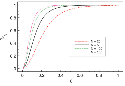
Figure 6 shows function versus with , for different numbers of interferometers (). At the destructive interference for produces a zero amplitude signal , leading to zero visibility. In the presence of the dephasing field the visibility rapidly increases and saturates to one, thereby revealing the coherence of the amplitude with respect to the phase .
Analogously, transmission probability is related to the amplitude of electrons exiting from the concatenated interferometers from channel . can be measured by tuning the beam splitter CS in Fig. 5 in order to swap inner and outer channels. One finds that
| (14) |
with , and visibility is defined analogously to (13). If we label () the mean value with respect to the phase of the transmission probability in 3 (4), we can write
| (15) |
In order to allow only a small fraction of the electron wavefunction to propagate in the dephasing channel and realize the conditions that allow IFMs, it is necessary to set the degree of admixture in the BS to the precise value . This may represent a technical obstacle to an experimental realization, since BSs are difficult to be tuned all to the same precise degree of admixture, and a high efficiency IFM is obtained in the limit of large . In the following we shall present a more robust architecture that allows one to overcome this difficulty by translating the spatial concatenation to the time-domain regime.
III Multiple interference in the time domain
In this section we show that it is possible to implement an IFM scheme based on the integer-quantum Hall Mach-Zehnder (MZ) interferometer of the type experimentally realized in Refs. [JiNature03, ; NederPRL06, ; LitvinPRB07, ; RoulleauPRB07, ; NederNatPh07, ; SamuelssonPRL04, ; NederNatur07, ] by exploiting a quantizing electron emitter Gabelli06 ; Feve07 ; Moskalets08 ; Splettstoesser08 .
Figure 7 shows a schematic view of the MZ interferometer, which comprises two beam splitters, two electrodes coupled through quantum point contacts (QPC1 and QPC2), and a dephasing source affecting the propagation of electrons in the edge channel . A small weakly-coupled circular cavity is placed between contact 1 and QPC1. This produces a train of time-resolved electron and hole wave packets (details of such single electron source can be found in Appendix A). Every period comprises a pair of electron and hole pulses, as shown in Fig. 10. QPC1 and QPC2 are controlled by the time-dependent external potentials and .
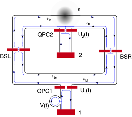
The system is operated as follows. In the first period, QPC1 is opened during the first half cycle letting the electron pulse to be injected into the MZ. It is closed during the second half so that holes will be reflected back into lead 1. The injected electron propagates with velocity along the edge of the MZ until it meets the first beam splitter BSL where it is split into two packets that follow two different edge channels ( and ) of equal length and finally reach the second beam splitter BSR after a time . Here the two packets interfere and then propagate along edges and of length . Keeping QPC1 and QPC2 closed, the sequence repeats itself with the electronic wavepacket being split and reunited many times at beam splitters BSL and BSR. This propagation is fully equivalent to a spatial concatenation of distinct MZ interferometers. At a chosen time, the electron pulse can be collected from leads 1 and 2 by opening QPC1 and QPC2, respectively.
Let us assume that an electron at time and a hole at time arrive at QPC1, with and , being the period of the cycle. The electron injected through QPC1 at time will appear at one of the two QPCs after a time , with , after performing rounds. The two QPCs are then opened simultaneously. In the case where no dephasing field is present, , it is possible to tune the MZ such that after rounds the electron pulse is at QPC2 and can be collected in contact 2. In the case of maximal dephasing, , the electron pulse is at QPC1.
Energy-level spacing inside the MZ can be estimated as . can be chosen to be large enough for a continuum approximation of the level spacing to be valid. This picture allows us to describe the physics in the Landauer-Büttiker formulation, with no needs of the Floquet treatment of this time-dependent problem. We introduce the electron annihilation operators that annihilate an electron on the edge states . In order to obtain the transport regime described in the previous section we must tune beam splitters BSL and BSR so that
| (16) |
with and , with the particular choice . Concerning the dynamical phase acquired by propagating along the edge channels, arms of equal length do not give rise to a relative phase shift, and the condition for the working point depends only on the applied magnetic-field intensity.
IV IFM with an Aharonov-Bohm ring
In this section we review the implementation of the IFM scheme using an asymmetric Aharonov-Bohm (AB) ring proposed in Ref. [NOI09, ] and discuss a scheme allowing the direct test of output-signal coherence. This latter task can be performed by embedding the asymmetric AB ring in a larger, symmetric AB ring. We shall examine the case in which the smaller ring is placed in the upper arm of the larger one, as shown in Fig. 8.
We shall use again the Landauer-Büttiker formalism of quantum transport and assume that the small asymmetric AB ring supports a single channel. Following Ref. [NOI09, ], we parametrize the scattering matrix connecting the incoming to the outgoing modes in node as
with , the bottom left block, the top right block and the remaining bottom right block, with and . Similarly, for node
| (17) |
We further assume injection invariance under node exchange. This configuration was theoretically studied and experimentally realized at low magnetic fieldsSzafranPRB05 ; SzafranEu05 ; Strambini09 and can be understood as the result of Lorentz force. We label annihilation operators for incoming and outgoing modes in node as and respectively, so that . Analogously we label incoming and outgoing modes in node as and , respectively, with . Symmetry under cyclic exchange of nodes and implies that
| (18) |
By rearranging the order of the vector components we obtain . controls the asymmetry of nodes and , so that for () complete asymmetry is achieved, with the electron entering from the left lead being injected totally in the lower (upper) arm, whereas for the injection is symmetric. An external magnetic field is applied perpendicularly to the plane and is responsible for the magnetic Aharonov-Bohm phase acquired in the ring. At the same time it yields the Lorenz force which leads to the ring asymmetry. Electron propagation in the two arms is described by matrices , for transmission from left to right, and , for transmission from right to left. Here is the ratio of the magnetic-field flux through the asymmetric ring to the flux quantum, is the Fermi wavenumber, is the length of the arms and is an additional random phase. In the following we shall set and anticipate that a different choice does not change qualitatively our findings.
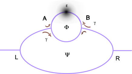
As mentioned earlier, the asymmetric AB ring is embedded in a larger symmetric AB ring so that the phase that an electron accumulates while traveling in the lower arm of the large ring represents a reference for the electron that traverses the asymmetric ring. By tuning the magnetic field that pierces the larger ring, we can determine the visibility of the current which reflects the loss of coherence occurring in the small asymmetric ring.
We describe scattering at nodes and of the large ring by a scattering matrix Buttiker84
| (19) |
with , the bottom left block, the top right block and the remaining bottom right block. The scattering matrix depends only on parameter , which controls the lead-to-ring coupling strength via , , , with . On the right node we have . Free propagation along the large-ring arms (assumed to be of equal length ) is accounted for by splitting the ring into two halves, each of which is described by the diagonal matrix , for propagation from left to right, and , for propagation from right to left. Here is the ratio of the magnetic-field flux through the larger symmetric ring () to the flux quantum. The overall amplitude for transmission from the left to the right lead is calculated through a multiple scattering formula which takes into account all interference processes between possible paths that electrons can take to go from the left to the right. In the absence of decoherence one finds (see Appendix C):
| (20) |
IV.1 Transmission in the presence of a dephasing field
We now assume a fluctuating external field (dephasing source) is placed in the upper arm of the small asymmetric ring. This can be described by defining the partial transmission amplitude of order with
| (21) |
where depends on two random phases and , and . As in Sec. II we then choose the random phases from a uniform distribution of zero mean and width and compute the averaged partial transmission probability as . It can be shown that the following recursive relation holds:
| (22) |
By iterating the procedure, the averaged transmission probability can be written as . To compute such limit we introduce the Gell-Mann matrix vector , with , write , with , and define the following decoherence matrix
| (23) |
which allows us to perform the average over the random phase as a matrix product. Similarly we define , and the decoherence map with entries
| (24) |
that describes the average over the random phase in . can be concisely written as
| (25) |
with the vector . By writing , with the eigenvalues of , the matrix of the eigenvectors of , and , that satisfy , we can perform the sum on obtaining
| (26) |
with being a matrix defined by The averaged transmission probability is now function of the AB phase .
IV.2 Current as a measure of coherence
The coherence of the signal transmitted through the small, asymmetric AB ring can be established by studying the transport properties of the entire device.
We focus on the case of strong coupling () for which an electron approaching the large ring from node is mostly transmitted into the two arms of the large ring ( in the following.) For clarity, we also set the magnetic field and the arm length so that , , , and . Actually, in a realistic experimental implementation it would be difficult to realize such conditions. We note however that the degree of coherence could be studied by changing one of the parameters of the large ring (e. g. ) and measuring the visibility of the oscillations of the output signal.
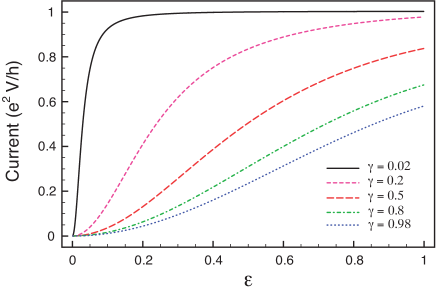
For an applied bias voltage , the zero-temperature current through the device of Fig. 8 is given by
| (27) |
with as in Eq. 26. Figure 9 shows as a function of the noise parameter for various values of the small-ring asymmetry parameter . As the dephasing strength is increased, however, increases with a behavior that strongly depends on the degree of asymmetry of the small ring. In the case of maximum decoherence () two different cases can be distinguished. For most of the electron amplitude that enters the small ring from the left will propagate into the lower arm of the small ring and coherently transmit into node R. There it interferes constructively with the reference path, saturating the current to the maximum . On the other hand for most of the electron amplitude that enters from the left into the small ring will propagate into the upper arm of the small ring. There a dephasing field is present and the signal that propagates through the small ring will combine at node R with the reference path. The current exiting the device reaches a maximal value between zero and . We interpret this behavior as an IFM of the dephasing field. The current exiting the device is proportional to the visibility of the output signal of the small asymmetric ring.
V Conclusion
Based on the idea first suggested in Ref. [NOI09, ] and directly inspired to the original proposal of A. Eliztur and L. Vaidman [ElitzurVaidman, ], in this article we focused on studying and detecting the presence of a classical external random fluctuating electric or magnetic field, which represent a common dephasing source in quantum devices. The noise source randomizes the phase of a propagating electron and plays the role of absorption in optical schemes while the loss of coherence of the outgoing electrons mimics photon absorption. The fraction of coherent output signal or alternatively the visibility of the outgoing signal represent the figures of merit that qualify an IFM. The study of this quantities allowed us to point out the difference between a “which-path” detection and an IFM: the former allows only the detection of the presence of a dephasing source at the expense of the degradation of the visibility of the outgoing signal, whereas the latter allows a coherent detection of the dephasing source.
Three distinct IFM schemes were investigated. The first system is a concatenation of interferometers based on the integer quantum Hall interferometric architecture proposed in Ref. [GiovannettiPRB08, ]. The dynamics of electrons traveling along edge channels is exposed to the action of an external fluctuating field. We suggest to steer the propagation of one channel towards the inner part of the Hall bar, where dephasing is minor or absent, and by separating and recombining many times the two channels we reproduce an electronic analogue of the high-efficiency scheme proposed in optics by P. Kwiat et al. in Ref. [KwiatPRL95, ]. We showed that, for a strong dephasing source, only an asymptotically negligible amount of coherent signal is lost by proper tuning the degree of admixture of the channels at the beam splitters. Moreover, the effect is very robust against small fluctuation about the exact value of the admixture required. Indeed, although the fraction of coherent signal is reduced in magnitude by the averaging process, its qualitative behavior is not affected by it.
The second system we considered is based on a standard quantum-Hall electronic Mach-Zehnder interferometer and assumes the presence of a quantized electron emitter. A very precisely time-resolved electronic wave packet is sent into a Mach-Zehnder interferometer in which an arm is affected by external classical noise. The packet travels at a precise speed and tests the region affected by noise many times, being split and recombined until it is allowed to escape the interferometer to be collected. The entire sequence can be mapped to the concatenation in the space domain that characterizes the noise-sensitive coherent electron channel previously described: the same results and conclusions apply also to this system. The latter has the advantage that it is experimentally much easier to realize, since it is based on a system already available.
The last system we considered is a double-ring structure based on the proposal suggested in Ref. [NOI09, ]. There, authors considered an Aharonov-Bohm chiral ring in which a localized source of noise affects one arm of the ring and studied the fraction of coherent signal that exits the device. However, such a quantity is not measurable in that setup. We suggest to embed the chiral AB ring in one arm of a larger AB ring and measure the total current flowing through the device as a figure of merit of the coherence of the output signal from the small chiral AB ring. Such a setup has the advantage to overcome the difficulties arising from concatenating many interrogation steps, necessary in order to achieve high efficiency IFM in the noise-sensitive coherent electron channel. It also eliminates the need for very precise time-resolved electronics, on which the second proposal was based.
We point out here that IFM can be designed also for the case of an electron absorber and the same results obtained with the dephasing source are found. The different implementations described here can find useful applications in quantum-coherent electronics and quantum computations, where the coherence of the signals is always threatened by the presence of fluctuating external fields.
This work was supported by funding from the German DFG within SPP 1285 “Spintronics”, from the Swiss SNF via grant no. PP02-106310, and by the Italian MIUR under the FIRB IDEAS project ESQUI. V. P. acknowledges CNR-INFM for funding through the SEED Program.
Appendix A Electron-hole switch
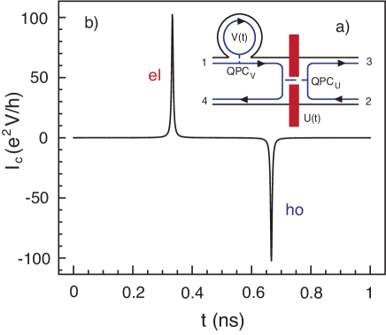
Let us consider the mechanism suggested in Sec. III for injecting and collecting electrons in the MZ interferometer. The system is depicted in Fig. 10 a) and is composed by a cavity formed by a circular edge state that is coupled to an edge channel by a QPCV of transmission amplitude and reflection amplitude . It was experimentally demonstratedGabelli06 ; Feve07 that such a device, if periodically driven by a time-dependent potential , produces a periodic current composed by an electron in one half-period and a hole in the other half-period, see Fig. 10 b). We wish to separate the electron and the hole by transmitting the electron through a barrier towards contact 3, and reflecting the hole into contact 4. A time-dependent QPCU driven by an external potential behaves like a beam splitter that mixes the incoming channels, from the contact 1 and 2, into the outgoing channels 3 and 4. If properly driven, it works as a switch that separates electrons and holes generated by the cavity into different edge channels. Following Refs. [Moskalets08, ; Splettstoesser08, ] we describe the effect of the time-dependent potential QPCU by a scattering matrix
| (28) |
In the symmetric case one has and . From the unitarity of follows that
| (29) | |||||
| (30) |
The dynamics of the cavity can be described by a time-dependent scattering amplitude , which satisfies . In the adiabatic regime, keeping all the reservoirs at the same chemical potential , the zero-temperature current in contacts 3 and 4 can be written as
| (31) |
with . Here is the current produced by the cavity, that can be written asMoskalets08 ; Splettstoesser08
| (32) |
is plotted in Fig. 10 b) for a harmonic driving , for the choice and . By defining and , it follows that and , with related to the applied external potential . By choosing a proper modulation of , it is possible to separate the electrons from the holes.
Appendix B Eigenvalue problem
Defining
| (33) |
The matrix assumes the simple form
| (34) |
with , that allows for a simple solution of the eigenvalue problem in terms of a Jordan decomposition, , with
| (35) | |||||
Appendix C Double ring transmission and reflection amplitudes
In the absence of decoherence, the transmission amplitude for electrons going from the left lead to the right lead can be calculated through the following multiple scattering formula
| (36) |
with , and . We define the following transmission matrices in node and that take into account the lower arm of the larger ring,
| (41) | |||||
| (46) |
with and of dimension , and and of dimension . Analogously we define the reflection matrices
| (51) | |||||
| (56) |
with and of dimension , and and of dimension . The effective transmission amplitudes and are given by the matrices
| (57) | |||||
| (58) |
with dimension respectively and . The effective reflection amplitudes and are given by the matrices
| (59) | |||||
| (60) |
References
- (1) A. Elitzur and L. Vaidman, Found. Phys. 23, 987 (1993).
- (2) P. Kwiat, H. Weinfurter, T. Herzog, A. Zeilinger, M. A. Kasevich, Phys. Rev. Lett. 74, 4763 (1995).
- (3) C. B. Chiu, E. C. G. Sudarshan, and B Misra, Phys. Rev. D 16, 520 (1977); B. Misra and E. C. G. Su- darshan, J. Math. Phys. 18, 756 (1977).
- (4) T. Tsegaye, E. Goobar, A. Karlsson, G. Björk, M. Y. Loh, and K. H. Lim, Phys. Rev. A 57, 3987 (1998).
- (5) A. G. White, J. R. Mitchell, O. Nairz, and P. G. Kwiat, Phys. Rev. A 58, 605 (1998).
- (6) E. H. du Marchie van Voorthuysen, Am. J. Phys. 64, 1504 (1996).
- (7) M. Hafner and J. Summhammer, Phys. Lett. A 235, 563 (1997).
- (8) P. G. Kwiat, A. G. White, J. R. Mitchell, O. Nairz, G. Weihs, H. Weinfurter, and A. Zeilinger, Phys. Rev. Lett. 83, 4725 (1999).
- (9) H. Paul and M. Pavicic, Int. J. of Th. Phys., 35 2085 (1996); J. Opt. Soc. Am. B 14, 1275 (1997); Found. of Phys. , 28 6 (1998).
- (10) J.-S. Jang, Phys. Rev. A 59, 2322 (1999).
- (11) S. Inoue and G. Björk, J. Opt. B: Quantum Semiclass. Opt. 2 338 (2000).
- (12) V. Giovannetti, S. Lloyd, and L. Maccone, Opt. Exp. 14, 8622 (2006).
- (13) M. O. Goerbig, Eprint arXiv:0909.1998.
- (14) Y. Ji, Y. Chung, D. Sprinzak, M. Heiblum, D. Mahalau, and H. Shtrikman, Nature (London) 422, 415 (2003).
- (15) I. Neder, M. Heiblum, Y. Levinson, D. Mahalu, and V. Umansky, Phys. Rev. Lett. 96, 016804 (2006).
- (16) L. V. Litvin, H. -P. Tranitz, W. Wegscheider, and C. Strunk, Phys. Rev. B 75, 033315 (2007).
- (17) P. Roulleau, F. Portier, D. C. Glattli, P. Roche, A. Cavanna, G. Faini, U. Gennser, and D. Mailly, Phys. Rev. B 76, 161309(R) (2007).
- (18) I. Neder, F. Marquardt, M. Heiblum, D. Mahalu, and V. Umansky, Nat. Phys. 3, 534 (2007).
- (19) P. Samuelsson, E. V. Sukhorukov, and M. Büttiker, Phys. Rev. Lett. 92, 026805 (2004).
- (20) I. Neder, N. Ofek, Y. Chung, M. Heiblum, D. Mahalu, and V. Umansky, Nature (London) 448, 333 (2007).
- (21) J. Gabelli, G. Fève, J.-M. Berroir, B. Plaçais, A. Cavanna, B. Etienne, Y. Jin, and D. C. Glattli, Science 313, 499 (2006).
- (22) G. Fève, A. Mahé, J.-M. Berroir, T. Kontos, B. Plaçais, D. C. Glattli, A. Cavanna, B. Etienne, and Y. Jin, Science 316, 1169 (2007).
- (23) M. Moskalets, P. Samuelsson, and M. Büttiker, Phys. Rev. Lett. 100, 086601 (2008).
- (24) J. Splettstoesser, S. Ol’khovskaya, M. Moskalets, and M. Büttiker Phys. Rev. B 78, 205110 (2008).
- (25) G. S. Paraoanu, Phys. Rev. Lett. 97, 180406(2006).
- (26) E. Strambini, L. Chirolli, V. Giovannetti, F. Taddei, R. Fazio, V. Piazza, and F. Beltram, accepted for publication in Phys. Rev. Lett., Eprint arXiv:0909.2197 [cond-mat.mes-hall].
- (27) F. Marquardt, and C. Bruder, Phys. Rev. B 65, 125315 (2002).
- (28) F. Marquardt, and C. Bruder, Phys. Rev. B 68, 195305 (2003).
- (29) F. Marquardt, and C. Bruder, Phys. Rev. Lett. 92, 056805 (2004).
- (30) V. Giovannetti, F. Taddei, D. Frustaglia, and R. Fazio, Phys. Rev. B 77, 155320 (2008).
- (31) M. Büttiker, Y. Imry, and M. Ya. Azbel, Phys. Rev. A 30, 1982 (1984).
- (32) M. Büttiker, Y. Imry, R. Landauer, and S. Pinhas, Phys. Rev. B 31, 6207 (1985).
- (33) M. Büttiker, Phys. Rev. B 38, 9375 (1988).
- (34) I. L. Aleiner, N. S. Wingreen, and Y. Meir, Phys. Rev. Lett. 79, 3740 (1997); E. Buks, et al., Nature 391, 871 (1998).
- (35) B. Szafran and F. M. Peeters, Phys. Rev. B 72, 165301 (2005)
- (36) B. Szafran and F. M. Peeters, Europhys. Lett. 70, 810 (2005).
- (37) E. Strambini, V. Piazza, G. Biasiol, L. Sorba, and F. Beltram, Phys. Rev. B 79, 195443 (2009).