*0.3truecm
Point-contact spectroscopy in heavy-fermion superconductors
Abstract
We develop a microscopic model to calculate point-contact spectra between a metallic tip and a superconducting heavy-fermion system. We apply our tunneling model to the heavy fermion CeCoIn5, both in the normal and superconducting state. In point-contact and scanning tunneling spectroscopy many heavy-fermion materials, like CeCoIn5, exhibit an asymmetric differential conductance, , combined with a strongly suppressed Andreev reflection signal in the superconducting state. We argue that both features may be explained in terms of a multichannel tunneling model in the presence of localized states near the interface. We find that it is not sufficient to tunnel into two itinerant bands of light and heavy electrons to explain the Fano line shape of the differential conductance. Localized states in the bulk or near the interface are an essential component for quantum interference to occur when an electron tunnels from the metallic tip of the point contact into the heavy-fermion system.
pacs:
74.55.+v, 74.70.Tx, 85.30.HiI Introduction
Point-contact (PCS) and scanning tunneling spectroscopies (STS) have been widely used to characterize the electronic behavior of heavy-electron materials, especially the transition into the superconducting state and the opening of an excitation gap. Unlike point-contact junctions with conventional metals, most heavy-fermion materials show asymmetric conductances, which have been difficult to explain. In addition to asymmetric normal-state conductances, many heavy-fermion superconductors (HFS) are known for strongly suppressed Andreev reflection signals. Nowack1987 ; DeWilde1994 ; Naidyuk1996 ; naidyuk1998 This is especially true for the heavy-fermion superconductor CeCoIn5. park2005 ; goll2005 ; goll2006 ; park2008a ; park2008b ; park09 Hallmarks of superconductivity are phase coherence and Andreev reflection (AR), which require the existence of a condensate of Cooper pairs. The AR signature occurs when a quasiparticle retro-reflects off a normal-superconducting (N/S) interface as a quasihole, while momentum and charge get carried across the interface by the Cooper pair.
The Blonder-Tinkham-Klapwijk (BTK) formulation describes the differential conductance in conventional N/S junctions remarkably well by invoking a dimensionless barrier strength parameter , which depends on the barrier potential and the mismatch ratio of Fermi velocities.btk For HFS this formula predicts that N/HFS junctions are in the tunneling limit, i.e., low transmission, and AR cannot occur, contrary to experimental observations. Attempts to correct this have been ad-hoc by postulating boundary conditions at the interface that are unaffected by the mass enhancement of the itinerant heavy electrons.Deutscher1994 Alternatively, a single heavy-band tunneling model with an energy-dependent quasiparticle lifetime was proposed to explain the strongly reduced AR signal, but it lacks to account for the large voltage asymmetry of the conductance in the normal state.Gloos1996 ; Anders1997
Over time various models for Kondo scattering without magnetic impurities have been proposed to explain point-contact studies ranging from tunneling into two-level tunneling systems coupled strongly to the conduction electrons Ralph1992 to localized electron spins at the point contact.Gloos2009 Very recently, Malteseva et al.Maltseva2009 presented a theory for electron cotunneling into a dense Kondo lattice that can account for a Fano line shape in the conductance. Also Yang Yang2009 argued that the PCS spectra for CeCoIn5 are consistent with a two-fluid picture based on the Kondo lattice scenario. Common shortcomings of all these approaches have been the ad-hoc nature of additional parameters to explain the PCS spectra, the neglect of localized states at the interface and the effects of pair-breaking surfaces in unconventional superconductors.
In this paper, we present a multichannel tunneling model for the solution of PCS and STS in heavy-fermion materials that is derived from an analysis of the PCS measurements of the heavy-fermion superconductor CeCoIn5. While we focus here on CeCoIn5 the proposed tunneling model has applications to heavy-fermion systems in general. For the first time, our multichannel tunneling model quantifies the reduced AR signal and conductance asymmetry observed in normal-metal/heavy-fermion superconductor (N/HFS) junctions without special constraints on tunneling barriers, Fermi velocity mismatch, or itinerant band mass renormalization at the interface.
The article is organized as follows: In Sec. II we introduce the multichannel tunneling model for the HFS and discuss specific limits. In Sec. III we present our theoretical results for a PCS junction and compare with several experimental PCS conductance curves varying over a wide range of voltage biases, temperature and orientations. Finally, we summarize our results in Sec. IV.
II Tunneling model
Our theoretical understanding of the normal-state properties of heavy-fermion materials is based on either the Kondo lattice or periodic Anderson model. The Kondo lattice model describes localized electronic magnetic moments at each lattice site coupled weakly to an itinerant electron band, while the periodic Anderson model describes localized -electrons hybridizing with itinerant electrons.Hewson1993 ; lohneysen2007
II.1 A microscopic model for heavy fermions
Solving the Kondo lattice or periodic Anderson model is a formidable task for multiorbital materials. Instead we model the heavy-fermion materials by two bands of itinerant electrons with localized surface states, which may be caused by broken -electron bonds at the surface due to the broken translation symmetry,
| (1) |
The heavy-fermion Hamiltonian represents two bands of itinerant conduction electrons with band index and localized electrons near the surface with site index . The operators () create (destroy) an itinerant electron with momentum and spin in band , while operators () create (destroy) an electron at site with spin . are the respective electronic dispersions and is the energy level of the localized electrons.
A simple description of a tunneling experiment is comprised of Hamiltonians for the heavy-fermion material, the counter electrode, and the transfer or tunneling processes between them: . The counter electrode is given by normal conduction electrons
| (2) |
and the tunneling Hamiltonian describes all possible transfers
| (3) | |||||
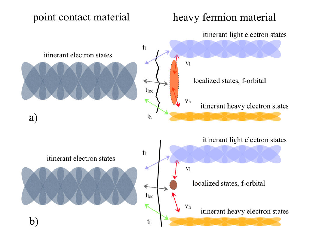
In addition to the standard overlap integrals between the conduction band in the point contact and itinerant heavy-fermion bands there is a finite overlap, , from the point contact to the localized states in the heavy fermion. We also account for weak interaction between the localized surface electrons and itinerant electrons through scattering terms (see Eq. 7 below). In general, to get a Fano resonance in the conductance one needs interference between different tunneling paths.fano1961 The resulting differential conductance calculated from this model will have an asymmetric Fano line shape. Our setup is similar to the one for scanning tunneling microscope (STM) tunneling through a magnetic atom on a metallic surface. madhavan1998 ; madhavan2001 ; Zhao2005 ; ternes2009 The difference between an STM and a point contact is that while the STM is defined by conduction through one or very few quantum channels a point contact consists of many conducting quantum channels in parallel. Figure 1 shows a cartoon of the processes that are active in tunneling between a metallic point contact and heavy-fermion material. Here we will extend the picture of conduction through individual quantum channels to a tunneling model to account for point contacts on a heavy-fermion material. We consider strong overlap between electron states in the contact and the heavy-fermion compound and thus go beyond the strict tunneling limit. We then extract microscopic model parameters in form of the overlap integrals and the energy of the localized state from fits made to the asymmetric conductances in the normal state of CeCoIn5 reported in the experiments by Goll et al.goll2005 ; goll2006 and Park et al.park2008a ; park2008b .
II.2 Tunneling current
To calculate the tunneling current through a quantum channel we employ the standard non-equilibrium Green’s function technique. Schrieffer1963 ; caroli1971 In Keldysh notation the tunneling current per conducting channel is given bycuevas2001
| (4) | |||||
The trace (Tr) is a short-hand notation for summation over momentum and spin , and the -product indicates a folding over common arguments, e.g., , and denotes the Keldysh component of the matrix Green’s function. Notation for matrices is: a ”hat” () denotes a Nambu matrix, while a ”check” () represents a Keldysh matrix (see below). For ease of readability, we suppress the explicit dependence of the tunneling elements and the Green’s function components on momentum and spin. In equation (4), are Green’s function components of the full matrix in reservoir space (=point contact, = light () and heavy () conduction bands of the HF, and is the localized state in the HF). It is the components of that straddle the interface (e.g. etc.) which enter equation (4). is to be determined in the presence of a voltage bias across the interface. The tunneling Green’s function is calculated by summing up single tunneling events in the self-consistent non-crossing approximation resulting in the Dyson equation
| (5) |
or equivalently
| (6) |
The transfer matrix , which is derived from the tunneling Hamiltonian , and sketched in Fig. 1, details all possible tunneling processes of electrons between the metallic tip, localized and itinerant electrons in the HFS,
| (7) |
Here are the wavefunction overlap integrals between contact and heavy-fermion material making up the tunneling elements between states and , while are surface-induced scattering elements between the localized state and the conduction bands in the heavy fermion material. CeCoIn5 is a very pure material with a mean-free path of order of 100 nm. Therefore, we assume that the junctions are in the ballistic limit where all tunneling events conserve momentum, i.e., .
To further simplify our calculations, we shall assume that the itinerant microscopic Green’s functions are described by quasiclassical Green’s functions near the Fermi energy, while it is essential to keep the full energy dependence of the localized Green’s function. In the case of non-superconducting electrodes the different unperturbed Green’s functions are
| (8) | |||||
| (9) | |||||
| (10) | |||||
with and is the third Pauli matrix in Nambu space. The distribution functions for the electrons are . The parameter gives the fraction of localized states and is a dimensionless quantity. The 22 Keldysh matrix structure of the Green’s functions and hopping element above is given as
| (15) | |||
| (20) |
For the Green’s function of the localized state, , we assume a single level at . To further simplify our model, we will assume that only the heavy electrons undergo a superconducting transition at , while the light electrons remain uncondensed. Similar arguments were entertained for the unconventional multiband superconductor Sr2RuO4, Agterberg1997 ; Graf2000 although one might expect, based on general grounds, that both bands go superconducting because of interband interactions leading to a proximity effect.Barzykin2007
The model of a single superconducting band may be justifiable for CeCoIn5, where no multiband gaps have been seen in the PCS data by Park et al.park2005 and Goll et al.goll2006 However, thermal conductivity measurements have been interpreted in terms of uncondensed electrons Tanatar2005 or fully paired electrons.Movshovich2001 ; Seyfarth2008 In this work, we shall take the view point that the light electrons remain uncondensed and explore the theoretical consequences for the PCS spectra. Thus for temperatures only the heavy electron Green’s function becomes
| (21) | |||||
with the self-consistently determined surface Green’s functions. It is worth noting that the surface Green’s functions are calculated in the quasiclassical approximation. They can fully account for surface pair-breaking due to the crystallographic orientation of the surface, disorder pair-breaking, and realistic band structure.bruder1990 ; buchholtz95 ; lofwander03 ; fogelstrom04 Surface pair-breaking can happen for anisotropic order parameters depending on the crystal orientation, but not for isotropic s-wave order parameters for which the standard BTK expressions were derived.
The are the usual (quasiclassical) retarded and advanced superconducting Green’s functions. Here we made the usual quasiclassical approximation of a constant density of states per unit energy and per spin for conduction electrons at the Fermi surface, both in the contact of the metal tip () and the heavy fermion (): . However, we kept the energy dependence of the localized density of states. To compactify our notation, we move the density of states factors and into the tunneling elements by re-writing , , . The new tunneling elements are dimensionless, while and have dimension .
Now we can solve through matrix inversion for the full Green’s function in Eq. (6). With the previous definitions we calculate the Green’s function components needed in the expression for the tunneling current in Eq. (4) through a point contact. First, we focus on the case of a heavy-fermion material in the normal state. For this case, we derive an analytic expression for the differential conductance for a single quantum channel, which leads to a modified Fano expression for the multiband tunneling model
| (22) | |||||
In Eq. (22) is the transparency, is the tunneling-renormalized position of the localized energy relative to the Fermi level, is the half-width of the resonance, and is the quantum interference parameter that controls the resonance shape. The additional parameter is present for multiband models only, when tunneling through a resonant localized state couples differently to the HF conduction bands (see below). adds a Lorentzian to the conventional Fano resonance which may be absorbed into a complex Fano parameter with . If one introduces the following two angles and and writes
| (23) | |||||
| (24) |
then the five phenomenological model parameters introduced in Eq. (22) depend on five microscopic parameters given by the following relations
| (25) | |||||
| (26) | |||||
| (27) | |||||
| (28) | |||||
| (29) |
The angle is a free parameter that quantifies the relative weight of the overlap integrals . cannot be determined from normal-state PCS measurements. The transparency of a single channel, , depends only on . The parameter is non-zero only if , i.e., . Finally, we see that in order to observe a Fano-shaped normal-state conductance, i.e., a finite , one needs to be in the limit of small to intermediate tunneling coupling, or , and have a sizable renormalization due to tunneling into the localized state, .
At this point we like to comment that the differential conductance derived in our multichannel tunneling model with localized nonmagnetic surface states, shown in Eq. (22), reduces to the Fano expression by YangYang2009 obtained for a Kondo lattice model with hybridized - electrons. Hence, we conclude that the observation of a Fano line shape in the conductance is not a sufficient condition for probing bulk electrons in the normal state. In order to associate the Fano peak with bulk electrons additional tests are necessary, e.g., observing the bare localized state crossing the Fermi level with temperature or a magnetic field dependence of the line width.
The PCS experiments measure a weak Fano-like conductance superimposed on a large background conductance . The asymmetry of the Fano shape in the conductance with respect to voltage accounts only for 3-5% of the total conductance. To capture both these contributions we need to go beyond the single quantum-channel conductance calculated in Eq. (22). Since a point contact forms over a sizable area, , compared to atomic scales (), one should expect thousands of channels present, each acting as a single quantum channel. The conductance should then be written as a sum over the contributions of the individual channels
| (30) |
The interface of a point contact is probably not atomically smooth, which means that the majority of localized states near the surface will be broadened to resonances due to destructive scattering in the interface (see panel (a) in Fig. 1). In the simplest case, this means that the localized state is broadened into a resonance as prescribed by . If the resonance is broad enough the conductance kernel in Eq. (22) gives only a broad and featureless contribution resulting in the background conductance. This applies to our analysis if meV is the largest energy scale of the problem. From these types of tunneling channels, i.e., those dominated by , Eq. (22) gives a weakly voltage-dependent background conductance . For the remaining few channels, the localized state forms a sharp surface state with , where is much smaller compared to other energies of the problem. To describe these channels we extract a phenomenological parameter from the PCS data ( is the fraction of channels having a sharp localized state at the interface). gives the proper magnitude of the Fano resonance relative to the background conductance. This bimodal distribution of two types of tunneling channels can be resolved in the normal state by numerical fits to the various data sets being considered here. For the tabulated values of and , see Table I, we find that their ratio () is typically between 3-5% for the point contacts we analyze. Another important point is that both and are only weakly temperature dependent, which indicates that the bimodal distribution of channels is a stable feature of each contact realization in a PCS experiment. Therefore the phenomenological differential tunneling conductance expression for a point contact accounting for this type of distribution of single quantum channels becomes
| (31) | |||||
The integrand in equation (31) depends on a set of four parameters that can be extracted from PCS experiments. These determine four microscopic parameters that depend on the transparency through the tunneling parameter . The factors are determined from the large voltage-scale conductance and in principle determine the distribution of channels . In what follows we will assume the simplest bimodal distribution of only two possible values of and . So far is the only model parameter undetermined by normal-state PCS data.
One should think about the sharp channels as a set of single-channel atomic point contacts. If we have a lattice mismatch between the tip and the HFS one may expect that a two-band model, as the one proposed here, should show a distribution of the angle . It seems natural to assume that the wavefunction of the tip may have different overlaps with each of the itinerant bands in the individual atomic point contacts, but still have a uniform transmission over the whole contact area. A consequence of this will be that different metallic tips, e.g., Au vs. Pt, should result in different overlaps with the itinerant bands of the HFS. We conclude that a more general formulation of the differential point-contact conductance should be written as
| (32) |
where is the distribution of and the (dI/dV)sharp is the numerically obtained conductance. Instead of modeling the distribution , we will look at PCS spectra for different values of .
II.3 Special limits of the tunneling conductance
The normal-state differential conductance in Eq. (31) has several instructive limits depending on the particular choice of microscopic model parameters. We consider the following four cases:
-
(a)
A one-channel tunneling model: Tunneling into one band only, i.e., and , reduces to the standard expression for a single channel contact with a transparency and a featureless differential conductance.The Fano parameters , , and all vanish, thus resulting in no Fano resonance. When the single band goes superconducting one obtains the standard Andreev conductance for HFS. This case corresponds to the special limit of () of the two-channel model to be discussed next.
-
(b)
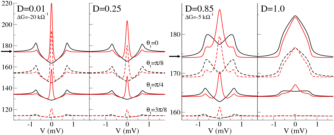
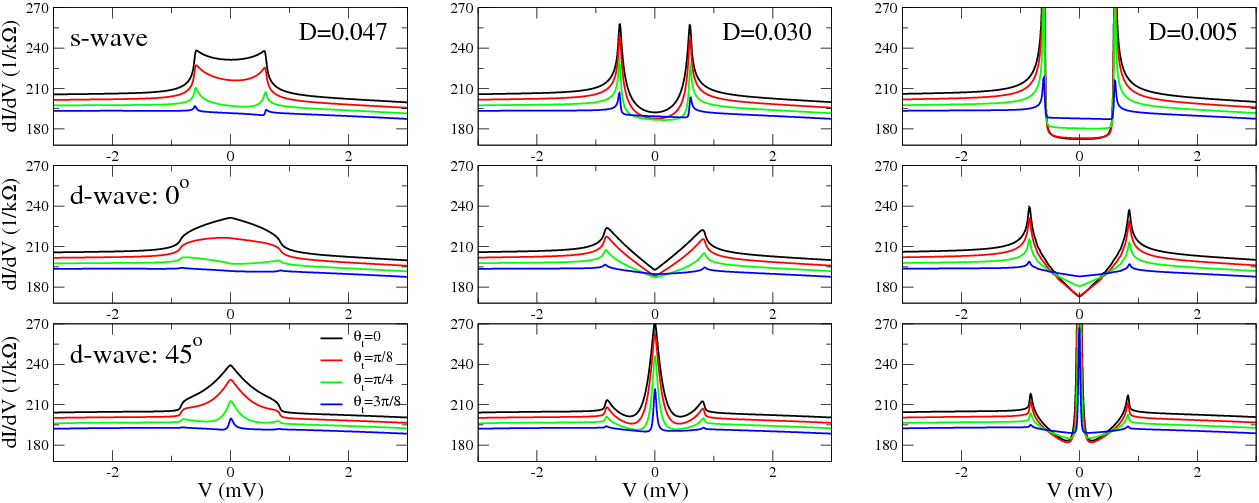
A two-channel itinerant tunneling model: Tunneling into both light and heavy bands but keeping will not generate a Fano resonance in the conductance as seen from Eqns. (25)-(29) with . In the normal state and for a constant density of states at the Fermi level in light and heavy bands, this limit gives a conductance which is constant. When the heavy band goes superconducting, , the two-band model gives an Andreev conductance, which may be reduced in signal with respect to the background conductance. In Fig. 2 we show conductances for fixed values of transparency , but with varying relative weight of the tunneling elements via the tunneling angle . The key result of these self-consistent calculations (for details see Sec. III.3) is that for high transparency junctions () and overwhelmingly tunneling into paired heavy electrons () it is impossible to differentiate between a -wave superconductor with nodal lines along [100] vs. [110]. Note that for the re-normalized tunneling matrix element for paired heavy and normal light electrons is equal. The situation is reversed for when tunneling is predominantly between the normal metallic tip and the normal light electrons in the HFS, see bottom curves in Fig. 2. This generic two-band tunneling model demonstrates that in principle PCS data can differentiate between tunneling preferentially into paired heavy electrons versus uncondensed light electrons.
-
(c)
A two-channel hybridized tunneling model: Simultaneously tunneling into a single itinerant band (here we consider a single heavy band, i.e., and ) and a localized state with nonzero scattering between localized and itinerant heavy electrons, i.e., and . This point-contact tunneling setup will generate a Fano resonance in the differential conductance with , for details see previous general Eqns. (25)-(29). Very recently, YangYang2009 discussed a Kondo lattice model of hybridized - electrons. He derived a normal-state Fano conductance similar to the one in our microscopic model in Eq. (22). In order to fit the Fano resonance in CeCoIn5, he introduced a voltage-dependent Fano parameter and a large interband term , which he attributed to multiband and correlation effects beyond - hybridization of electrons. Assuming a constant implies a strongly temperature dependent interband scattering coefficient , which is difficult to reconcile within our model. Furthermore, as we have shown above, introducing a nonzero is equivalent to introducing asymmetric scattering between different itinerant bands and localized states, , invalidating the model assumption of only two species of electrons used in the standard Kondo lattice model with only - hybridization.
-
(d)
A multichannel tunneling model: Simultaneously tunneling into localized and itinerant bands is of topic interest and will be discussed in the next section.
III Results and Discussion
We take the following approach for extracting the microscopic tunneling elements from point-contact conductance data: We fit the differential conductance in Eq. (31) to an experimental dI/dV-curve at a given temperature by extracting all model parameters, i.e., the four Fano parameters , the relative weight of the Fano-like conductance , and the background conductance . After extracting the set of phenomenological parameters () through numerical fits, we solve for the set of microscopic parameters () by treating and as free fit parameters. Consequently, the parameters or equivalently and can only be determined by studying the conductance in the superconducting state as they effectively drop out from the normal-state conductance, see Eq. (31).
III.1 Model parameters in the normal state
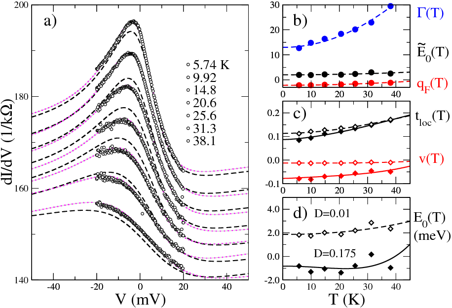
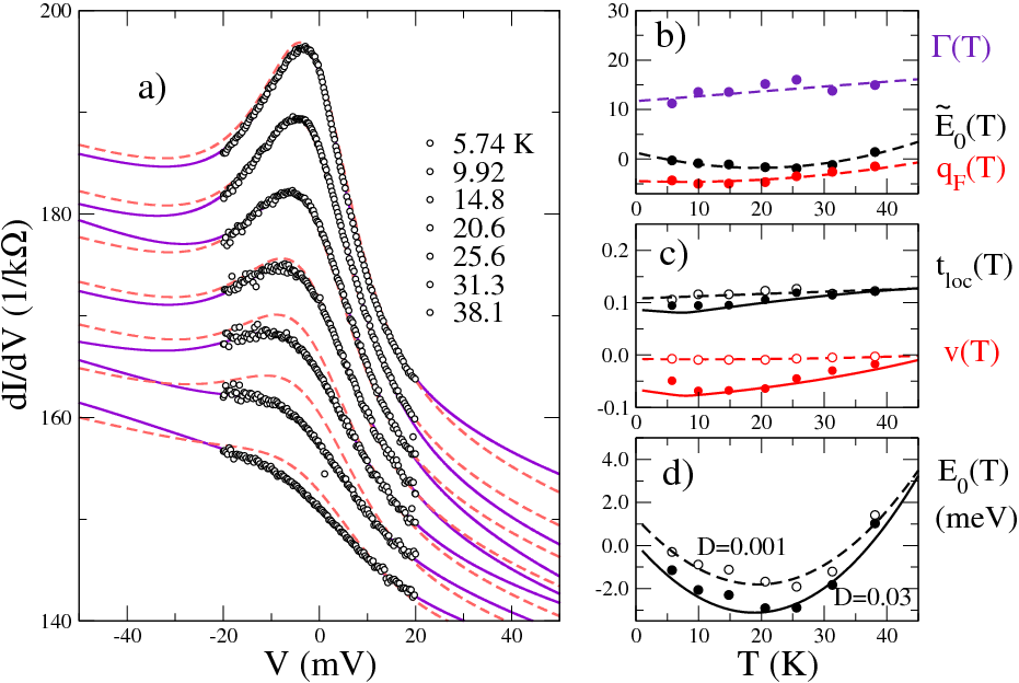
In Figs. 3 and 4, we show results extracted from a set of conductances taken at different temperatures using a Au-tip on -oriented CeCoIn5. For each individual dI/dV-curve we get a good fit to a Fano resonance over the entire measured voltage window of 20 mV. We note that while the dI/dV-curves are well fitted within the chosen voltage window in both Figs. 3 and 4 the extrapolated large voltage-scale conductances are very different as we assumed a constant background in Fig. 3, while in Fig. 4 we modeled the background conductance as , where is an additional parameter that is always of the order of the voltage window and will not be considered any further. As seen in these figures, the Fano parameters depend sensitively on the details of how the background conductance is modeled. Therefore, for deriving meaningful Fano parameters from PCS measurements it is very important to measure over voltage biases as large as possible while at the same time avoiding heating.
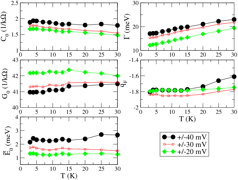
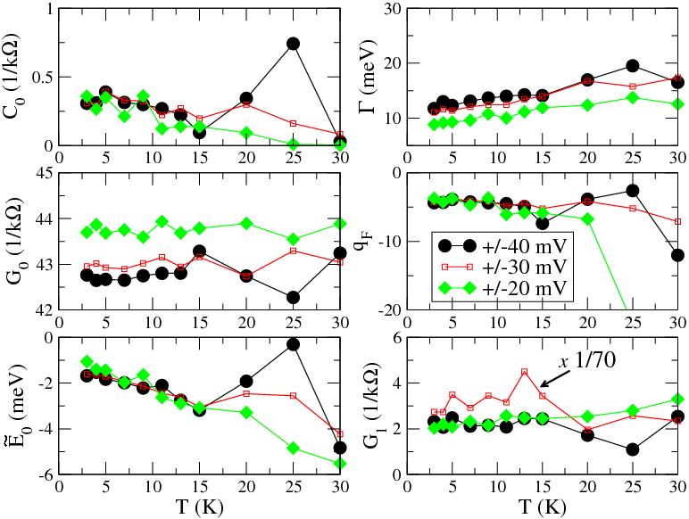
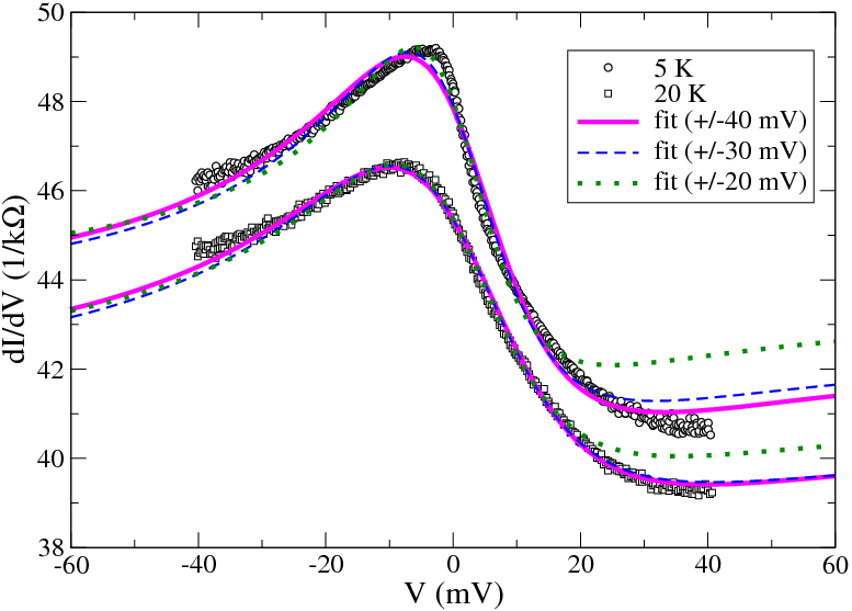
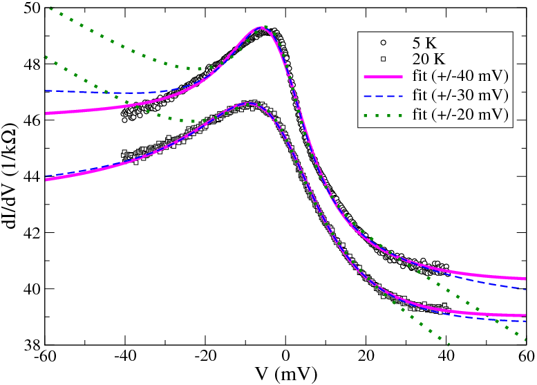


The model parameters () all have a temperature dependence that may be fitted with a polynomial , with or and is a typical temperature scale for the onset of the strongly correlated heavy-fermion state. For CeCoIn5 we set =45 K. When we re-calculate the dI/dV-curves with the fitted temperature dependent model parameters, we find that the goodness of a single fit is sensitive to the precise values of , and . These re-calculated dI/dV-curves are shown as dashed lines in Figs. 3 and 4, whereas the fits with the original parameter sets are shown as dotted lines.
In Figure 5 we show the temperature dependence of the model parameters, when PCS data are collected over a larger voltage bias window. We discover that (i) the parameters depend significantly on the size of the voltage bias window over which the fit is performed, although they exhibit similar temperature trends; (ii) the interband scattering parameter is not uniquely determined (not shown). Only the localized level , Fano line half-width , and Fano parameter are insensitive to . The transparency parameter is weekly dependent on . Since the parameter has negligible impact on fitting the conductance, we set for the remainder of this work.
Quite unexpectedly, we find that the magnitudes and temperature dependences of the phenomenological model parameters depend strongly on the treatment of the conductance background. The only robust feature that can be extracted is a temperature dependent Fano parameter of order 16 meV that nearly doubles between 5 K and 30 K. All other parameters depend on the background modeling. The extracted temperature dependence of suggests the importance of inelastic scattering at elevated temperatures. Spin-fluctuations seen in NMR measurements of CeCoIn5 and related materials are likely sources for this behavior.Kawasaki2003 ; Curro2005 The renormalized localized level is either positive (above the Fermi level) and nearly independent of temperature (constant background ) or negative (possibly below the Fermi level) and decreases further with increasing temperature (-dependent background). We do not observe a crossing of the localized bare level from positive to negative as temperature is increased. This suggests that the localized states are most likely surface states, since for bulk states localized electron levels should be pushed below the Fermi level for temperatures higher than a characteristic heavy-fermion coherence temperature . Above 45 K the heavy-fermion system CeCoIn5 exhibits well-developed localized moments.
To further characterize the origin of the resonance, spectroscopic measurements at higher temperatures and in magnetic fields may distinguish between localized magnetic Kondo states in a latticePines2008 ; Curro2004 and nonmagnetic surface states. Currently the picture is not clear. If the resonance originates from the Kondo lattice effect, one would expect that the resonance disappears above the Kondo lattice (coherence) temperature K in CeCoIn5. However, this characteristic temperature is only one quarter of what is expected from the half-width of the resonance meV or K. Additionally, it has been suggested that a magnetic field splits the Kondo resonance due to the Zeeman effect. However, there is no indication that fields as high as 9 T affect the conductance.park09 ; goll2006b
In Figure 6 we show selected normal-state conductance fits for CeCoIn5 at 5 K and 20 K that were used to extract the model parameters shown in Fig. 5. These fits highlight the need for conductance measurements over voltage biases as large as possible, because fitting a Fano resonance over a small voltage window leads to significant deviations outside that region and hence quite different model parameters.
| expt. | Parameter | |||||
| [meV] | [meV] | [] | [] | |||
| Fig. 3 | 2.01 | 13.0 | -2.16 | 5.6 | 163 | |
| 1.08 | 22.5 | 1.59 | 2.1 | 2.7 | ||
| Fig. 4 | 1.30 | 11.7 | -4.44 | 1.66 | 166 | |
| -14.2 | 4.42 | -1.92 | -3.29 | 3.81 | ||
| 16.4 | 0 | 5.67 | 4.11 | -0.07 |
In Table 1 we report the temperature dependent model parameters for data shown in Figs. 3 and 4. From this analysis we find that the only robust Fano parameter is , which measures the half-width of the Fano resonance, while all other parameters vary from measurement to measurement and depend on the background fit, see Figs. 3, 4 and 5. The temperature behavior of the renormalized parameter for the localized level can vary from nearly flat to decreasing or increasing with increasing temperature depending on the treatment of the background conductance. No universal behavior can be identified that might relate to the bulk properties of CeCoIn5, as argued within a two-fluid interpretation of the PCS data. Pines2008 ; Yang2009 How to disentangle surface from bulk effects remains a challenge. It should be possible, in principle, to observe the nature of the correlated electronic state and the dualityPNAS2008 of electrons in CeCoIn5 with tunneling experiments.
III.2 Model parameters in the superconducting state
When a material shows superconductivity one can use the nonlinear voltage dependence of its N/S conductance to extract further information about the undetermined parameters (or ) and . In Fig. 7(a) we plot the calculated transparency as a function of for the conductances fitted in Fig. 3. In panels (b)-(d) we show the corresponding conductances calculated at 0.1 K (CeCoIn5 has a K) using the extracted temperature dependent model parameters with an s-wave order parameter. In panel (e) we show the self-consistent BTK N/S-conductance btk superimposed on the normal-state conductance as
| (33) |
for the full range of transparencies . Here is the fraction of sharp channels in accordance with the model for PCS described by equation (31). The self-consistent BTK N/S-conductance, , is computed using quasiclassical Green’s functions as done in Refs. laube00, ; laube04, by accounting explicitly for surface pair-breaking, which goes beyond the standard BTK formulation. Therefore our self-consistent method enables the determination of the spectral properties of the superconducting state by incorporating pair-breaking through surface scattering for anisotropic order parameters, elastic impurity scattering, and inelastic scattering off from low-frequency bosonic modes.
In panels (b)-(d) of Fig. 7, we vary the heavy-light electron tunneling angle allowing for competition between tunneling into a normal conducting and a superconducting band in the heavy-fermion material. As seen, the N/S conductance is sensitive to both the transparency and , i.e., the relative ratio of tunneling into the superconducting vs. the normal-state band. Tunneling through a resonant state enhances the effective transparency of the junction, so that a has an N/S conductance similar to a BTK conductance of transparency . We also see in Figs. 7 and 8 that for junctions with ”high” transparency , the sub-gap conductance is enhanced. Another crucial result of this multichannel model is that the conductance enhancement due to AR is only relative to the normal-state conductance and not the conventional . Note that the suppression of the AR signal in the HFS comes naturally about by tunneling into either multiple bands or through localized states into one heavy band. Hence the reduction of the AR signal can be due to not being aligned with the Fermi level and tunneling is slightly off-resonant. In turn this leads to an incomplete Andreev reflection as there is a slight particle-hole asymmetry with respect to (see in Eq. (10)). No ad-hoc postulates are required for the Fermi velocity mismatch between point-contact tip and HFS or special boundary conditions at the interface. Instead it is accounted for in the tunneling matrix elements of the wavefunction overlap between the metallic tip and the HFS.
III.3 Symmetry of the superconducting order parameter
There is quite a body of evidence that the heavy-fermion material CeCoIn5 is an unconventional superconductor with a d-wave symmetry of the order parameter.Movshovich2001 ; Izawa2001 ; Curro2002 ; Capan2004 ; Aoki2004 ; Tanatar2005 ; Seyfarth2008 ; park09 ; An2010 We follow the strategy outlined in Refs. buchholtz95, ; lofwander03, ; fogelstrom04, ; laube00, ; laube04, and use the quasiclassical theory to compute self-consistently the surface states of a d-wave superconductor. The surface Green’s function is then used to evaluate the conductance taking into account surface pair-breaking and hence a reduced order parameter at the surface. We emphasize that surface pair-breaking of the order parameter is not included in the original BTK formulation and hence will lead to differing results. The results of our self-consistent calculations are shown in Fig. 8 using the same model parameters as in Fig. 7 As seen in panels (a)-(c) we have a sensitive dependence on the surface orientation relative to the crystal axis orientation.tanaka95 If the surface normal is aligned with the crystal axis along which the d-wave order parameter has a lobe , then the conductance shows qualitatively the same shape as an s-wave superconductor, especially if one takes into account the trajectory-average over the order parameter . If the surface normal is misaligned with the crystal-axis the surface is pair-breaking for a d-wave superconductor as the surface scattering connects trajectories with different order parameter values, i.e., . For trajectories where the order parameter changes sign there is a zero-energy Andreev bound state,Buchholtz1981 ; Hu94 which gives rise to a zero-bias conductance peak.tanaka95 Therefore the NS-conductance in a d-wave superconductor will depend on the principal tunneling direction a point contact or STM tip has relative to the crystal orientation. In panel (d) in Fig. 8 we show the self-consistent BTK-conductance computed with Eq. (33) using the superconducting fraction . For there is a clear dependence on the surface-to-crystal orientation. For fully transparent contacts on the other hand there is very little difference between a contact and one with . For the dI/dV-curves calculated using the model parameters we never reach the fully transparent limit, as for the s-wave case in Fig. 7, the resonant enhancement of tunneling via a localized state gives for a sub-gap conductance similar to that of the self-consistent BTK scenario with . For smaller the tunneling limit is approached.
The high transmission case, , gives good agreement between the self-consistent BTK conductance and experimental datapark2008a ; park2008b at all temperatures below irrespective of surface-to-crystal orientation , see Fig. 8. Similarly, the conductances calculated with the multichannel tunneling model reproduce to a large extent the experimental PCS data, as can be seen in Figs. 8 and 9. In Fig. 9 we show the corresponding conductance curves for an s-wave and d-wave superconductor in the presence of a voltage-dependent background , where the model parameters are extracted form normal-state fits shown in Fig. 4. It is clear from these self-consistent calculations that PCS measurements should be able to differentiate between tunneling into the nodal vs. the antinodal direction of the gap function, irrespective of the transparency of the junction. Further, in the Fano scenario we find that the amplitude of the conductance in the sub-gap region has the proper suppressed magnitude compared to the background. The suppression is a direct consequence of either competing or interfering tunneling channels.
A key result of these self-consistent calculations is that a modified expression for the BTK conductance for an HFS point-contact junction, see Eq. (33), gives the correct description of experiment. However, an unphysical parameter , i.e., tunneling in the high transmission limit, is required. On the other hand, the multichannel tunneling model gives the correct description with physically reasonable microscopic parameters, i.e., tunneling in the low transmission limit with .
IV Conclusions
In summary, we developed a microscopic tunneling model for heavy-fermion materials. A narrow spectroscopic feature associated with localized states seen in the heavy-fermion material CeCoIn5 is modeled through a multichannel tunneling junction. The asymmetric line shape of the differential conductance is understood as a Fano resonance for localized states in the vicinity of the interface coupled with itinerant heavy electrons in the bulk of CeCoIn5.
We list the key results of our analysis:
-
•
The generic two-channel itinerant tunneling model demonstrates that in principle PCS data can differentiate between tunneling preferentially into paired heavy electrons versus uncondensed light electrons.
-
•
A consequence of the self-consistent calculations for the two-channel itinerant tunneling model in the absence of localized states is that for high transmission junctions () and overwhelmingly tunneling into paired heavy electrons () it is impossible to differentiate between a -wave superconductor with nodal lines along [100] vs. [110].
-
•
The only robust Fano parameter, we succeeded to extract from several PCS measurements on different samples, is with meV. It measures the half-width of the Fano resonance. Its temperature behavior suggests the presence of significant inelastic scattering, which may be due to self-energy effects like scattering off from spin fluctuations or electrons.
-
•
Finally, for a multichannel tunneling model the zero-bias conductance enhancement due to Andreev reflection is reduced to only relative to the normal-state conductance compared to the conventional 100% effect. The origin of this suppression can be due to either tunneling into multiple competing itinerant bands or through a localized state into one itinerant band.
We conclude that it is desirable to have tunneling measurements ranging from the low to high transmission limit. Future measurements at higher magnetic fields, higher temperatures, and over wider voltage bias windows will help to probe quantum interference of electrons tunneling between a metallic tip and itinerant heavy-fermion bands. In order to identify the origin of the localized states nanosized PCS tips or STM tips, which are in the single-quantum channel limit for tunneling, will prove to be critical for resolving the mystery of tunneling into heavy-fermion materials. Since our microscopic multichannel tunneling model is quite generic, it should also be applicable to other heavy-fermion materials.
V Acknowledgments
We are indebted to T. Löfwander for insightful discussions early in this work, and especially like to thank V. Siderov, J. Thompson, R. Movshovich, and Y. Yang for discussions during later stages of this work. M. F. was supported by the Swedish Research Council, W. K. P. and L. H. G. were supported by the U.S. DOE under award No. DE-FG02-07ER46453 through FSMRL and CMM at UIUC, and M. J. G. was supported in part by the U.S. DOE at Los Alamos National Laboratory under contract No. DE-AC52-06NA25396 and the UC Research Program.
References
- (1) A. Nowack, A. Heinz, F. Oster, D. Wohlleben, G. Güntherodt, Z. Fisk, and A. Menovsky, Phys, Rev. B. 36, 2436(R) (1987).
- (2) Y. De Wilde, J. Heil, A. G. M. Janse, P. Wyder, R. Deltour, W. Assmus, A. Menovsky, W. Sun, and L. Taillefer, Phys. Rev. Lett. 72, 2278 (1994).
- (3) Yu. G. Naidyuk, H. v. Löhneysen, G. Goll, I. K. Yanson, and A. A. Menovsky, Europhys. Lett. 33, 557 (1996).
- (4) Yu. G. Naidyuk and I. K. Yanson, J. Phys. Condens. Matter 10, 8905 (1998).
- (5) W. K. Park, L. H. Greene, J. L. Sarrao, and J. D. Thompson, Phys. Rev. B 72, 052509 (2005).
- (6) G. Goll, Adv. Sol. State Phys. 45, 213 (2005).
- (7) G. Goll, T. Brugger, M. Marz, S. Kontermann, H. v. Löhneysen, T. Sayles, M. B. Maple, Physica 378-380B, 665 (2006).
- (8) W. K. Park, J. L. Sarrao, J. D. Thompson, and L. H. Greene, Phys. Rev. Lett. 100, 177001 (2008).
- (9) W. K. Park, E. D. Bauer, J. L. Sarrao, J. D. Thompson, and L. H. Greene, J. Phys: Conf. Ser. 150, 052207 (2009).
- (10) W. K. Park and L. H. Greene, Journal of Physics: Condensed Matter 21, 103203 (2009).
- (11) G. E. Blonder, M. Tinkham, T. M. Klapwijk, Phys. Rev. B. 25, 4515 (1982).
- (12) G. Deutscher and P. Noziéres, Phys. Rev. B 50, 13557 (1994).
- (13) K. Gloos, F. B. Anders, B. Buschinger, C. Geibel, K. Heuser, F. Jährling, J. S. Kim, R. Klemens, R. Müller-Reisener, C. Schank, and G. R. Stewart, J. Low Temp. Phys. 105, 37 (1996).
- (14) F. B. Anders and K. Gloos, Physica B 230-232, 437 (1997).
- (15) D. C. Ralph and R. A. Buhrman, Phys. Rev. Lett. 69, 2118 (1992).
- (16) K. Gloos, Low Temp. Phys. 35, 935 (2009).
- (17) M. Maltseva, M. Dzero, and P. Coleman, Phys. Rev. Lett. 103, 206402 (2009).
- (18) Y. F. Yang, Phys. Rev. B 79, 241107(R) (2009).
- (19) A. C. Hewson, The Kondo Problem to Heavy Fermions (Cambridge Univ. Press, 1993).
- (20) H. v. Löhneysen, A. Rosch, M. Vojta, and P. Wölfle, Rev. Mod. Phys. 79, 1015 (2007).
- (21) U. Fano, Phys. Rev. 124, 1866 (1961).
- (22) V. Madhavan, W. Chen, T. Jamneala, M. F. Crommie, and N. S. Wingreen, Science 280, 567 (1998).
- (23) V. Madhavan, W. Chen, T. Jamneala, M. F. Crommie, and N. S. Wingreen, Phys. Rev. B 64, 165412 (2001).
- (24) A. Zhao, Q. Li, L. Chen, H. Xiang, W. Wang, S. Pan, B. Wang, X. Xiao, J. Yang, J. G. Hou, and Q. Zhu, Science 309, 1542 (2005).
- (25) M. Ternes, A. J. Heinrich, and W. Schneider, J. Phys. Condens. Matter 21, 053001 (2009)
- (26) J. R. Schrieffer and J. W. Wilkins, Phys. Rev. Lett. 10, 17 (1963).
- (27) C. Caroli, R. Combescot, P. Nozieres, D. Saint-James, Journal of Physics C: Solid State Physics 4, 916 (1971).
- (28) J.C. Cuevas, A. Martín-Rodero, and A. Levy Yeyati, Phys. Rev. B 54, 7366 1996; J. C. Cuevas and M. Fogelström, Phys. Rev. B 64 104502 (2001)
- (29) D. Agterberg, T. M. Rice, and M. Sigrist, Phys. Rev. Lett. 78, 3374 (1997).
- (30) M. J. Graf and A. V. Balatsky, Phys. Rev. B 62, 9697 (2000).
- (31) V. Barzykin and L. P. Gor’kov, Phys. Rev. B 76, 014509 (2007).
- (32) M. A. Tanatar, J. Paglione, S . Nakatsuji, D. G. Hawthorn, E. Boaknin, R. W. Hill, F. Ronning, M. Sutherland, L. Taillefer, C. Petrovic, P. C. Canfield, and Z. Fisk, Phys. Rev. Lett. 95, 067002 (2005).
- (33) R. Movshovich, M. Jaime, J. D. Thompson, C. Petrovic, Z. Fisk, P. G. Pagliuso, and J. L. Sarrao, Phys. Rev. Lett. 86, 5152 (2001).
- (34) G. Seyfarth, J. P. Brison, G. Knebel, D. Aoki, G. Lapertot, and J. Flouquet, Phys. Rev. Lett. 101, 046401 (2008).
- (35) C. Bruder, Phys. Rev. B 41, 4017 (1990)
- (36) L. J. Buchholtz, M. Palumbo, D. Rainer, and J. A. Sauls, J. of Low Temp. Phys. 101, 1079 (1995); ibid 101, 1099 (1995)
- (37) T. Löfwander, M. Fogelström, and J. A. Sauls, Phys. Rev. B 68, 054504 (2003)
- (38) M. Fogelström, D. Rainer, and J. A. Sauls, Phys. Rev. B 70, 012503 (2004)
- (39) Y.-F. Yang and D. Pines, Phys. Rev. Lett. 100, 096404 (2008).
- (40) N. J. Curro, B.-L. Young, J. Schmalian, and D. Pines, Phys. Rev. B 70, 235117 (2004).
- (41) G. Goll, Physica B, 383, 71 (2006).
- (42) T. Park, M. J. Graf, L. Boulaevskii, J. L. Sarrao, and J. D. Thompson, Proc. Nat. Acad. Sci. 105, 6825 (2008).
- (43) F. Laube, G. Goll, H. v. Löhneysen, M. Fogelström, and F. Lichtenberg, Phys. Rev. Lett. 84, 1595 (2000).
- (44) F. Laube, G. Goll, M. Eschrig, M. Fogelström, and R. Werner, Phys. Rev. B. 69, 014516 (2004).
- (45) N. J. Curro, B. Simovic, P. C. Hammel, P. G. Pagliuso, G. B. Martins, J. L. Sarrao, and J. .D Thompson, Phys. Rev. B 64, 180514 (2002).
- (46) C. Capan, A. Bianchi, R. Movshovich, A. D. Christianson, A. Malinowski, M. F. Hundley, A. Lacerda, P. G. Pagliuso, and J. L. Sarrao, Phys. Rev. B 70, 134513 (2004).
- (47) K. Izawa, H. Yamaguchi, Y. Matsuda, H. Shishido, R. Settai, and Y. Onuki, Phys. Rev. Lett. 87, 057002 (2001).
- (48) H. Aoki, T. Sakakibara, H. Shishido, R. Settai, Y. Onuki, P. Miranović, and K. Machida, J. Phys.: Condens. Matter 16, L13-L19 (2004).
- (49) K. An, T. Sakakibara, R. Settai, Y. Onuki, M. Hiagi, M. Ichioka, and K. Machida, Phys. Rev. Lett. 104, 037002 (2010).
- (50) Y. Tanaka and S. Kashiwaya, Phys. Rev. Lett. 74, 3451 (1995).
- (51) L. J. Buchholtz and G. Zwicknagl, Phys. Rev. B. 23, 5788 (1981).
- (52) C. R. Hu, Phys. Rev. Lett. 72, 1526 (1994).
- (53) Y. Kawasaki, S. Kawasaki, M. Yashima, T. Mito, G.-q. Zheng, Y. Kitaoka, H. Shishido, R. Settai, Y. Haga, and Y. Ŏnuki, J. Phys. Soc. Jpn. 72, 2309 (2003).
- (54) N. J. Curro, T. Caldwell, E. D. Bauer, L. A. Morales, M. J. Graf, Y. Bang, A. V. Balatsky, J. D. Thompson, and J. L. Sarrao, Nature (London) 434, 622 (2005).