Energy bands, conductance and thermoelectric power for ballistic electrons in a nanowire with spin-orbit interaction
Abstract
We calculated the effects of spin-orbit interaction (SOI) on the energy bands, ballistic conductance () and the electron-diffusion thermoelectric power () of a nanowire by varying the temperature, electron density and width of the wire. The potential barriers at the edges of the wire are assumed to be very high. A consequence of the boundary conditions used in this model is determined by the energy band structure, resulting in wider plateaus when the electron density is increased due to larger energy-level separation as the higher subbands are occupied by electrons. The nonlinear dependence of the transverse confinement on position with respect to the well center excludes the “pole-like feature” in which is obtained when a harmonic potential is employed for confinement. At low temperature, increases linearly with but deviates from the linear behavior for large values of .
pacs:
73.23.Ad, 75.70.Tj,81.07.GfI Introduction
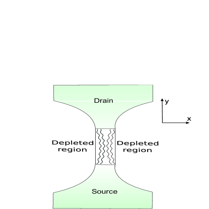
The electronic transport and photonic properties of a two-dimensional electron gas (2DEG) such as that found at a semiconductor heterojunction of GaAs/AlGaAs have been the subject of interest and discussion for many years now. davies Related physical properties of narrow quantum wires of 2DEG have also been the subject of experimental and theoretical investigations because of their potential for device applications in the field of nanotechnology. pepper1 ; pepper2 It is thus necessary to specify the model for the edge of a narrow quantum wire. moroz ; privman ; gumbs1 Here, we analyze the role played by the boundaries on the ballistic electron transport in a nanowire of 2DEG where the Rashba spin-orbit interaction (SOI) is included. The role of SOI on collective properties of the 2DEG has been investigated. manvir ; gumbs ; go The quasi-one-dimensional channel may be formed by applying a negative bias to a metal gate placed on the surface and depleting the 2DEG below it. Alternatively, the quasi-one dimensional channel may be made by etching all the way down to the active layer.In either way, it has been demonstrated that the width of the wire could influence the electron transport properties. pepper1 ; pepper2 In the latter case, the edges are sharper and may be appropriately modeled by sharp and high boundary conditions. More recently, Brey and Fertig fertig have pointed out that graphene nanoribbons have different collective plasmon dispersion relations depending on whether they have armchair or zigzag edges.
It is well established that the spin-orbit coupling is an essentially relativistic effect: an electron moving in an external electric field sees a magnetic field in its rest frame. In a semiconductor, the interaction causes an electron’s spin to precess as it moves through the material, which is the basis of various proposed “spintronic” devices. In nano-structures, quantum confinement can change the symmetry of the spin-orbit interaction. The relativistic motion of an electron is described by a Dirac equation. These effects combine to form both an electric dipole moment and the Thomas precession which is due to the rotational kinetic energy in the electric field. darwin ; fisher The two mechanisms accidentally have very close mathematical form and consequently combine in a very elegant way. The SOI Hamiltonian can be obtained from the Dirac equation by taking the non-relativistic limit up to terms quadratic in . This limit can be achieved either by expanding the Dirac equation in powers of or by making use of the asymptotically exact Foldy-Wouthousen transformation. foldy
We include the effects due to edges through sharp and high potentials at the boundaries. As a result, we are not able to solve the Rashba SOI model Hamiltonian to obtain analytic solutions for the eigenenergies and eigenfunctions. The reason for this is due to the fact that the solution manifestly contains quantum interference effects from multiple scattering off the edges. We solved the eigenvalue problem numerically, obtaining the energies as a function of the wave vector parallel to the edge of the nanowire shown schematically in Fig. 1. This model for the edges is different from that employed in previous works. moroz ; privman ; gumbs1 We calculate the ballistic conductance and the electron-diffusion thermoelectric power for this quasi-one-dimensional structure by assuming that the length of the channel between source and drain is less than the electron mean free path. In addition, we assume that the width of the channel is of the order of the de Broglie wavelength. Beenakker
The outline of the rest of this paper is as follows. In Sec. II, we present our model for the wide quantum wire with spin-orbit coupling and specified boundary conditions to simulate the effects arising from the edges of the nanowire. We also present numerical results for the energy bands in order to study the combined effect of the boundaries and the SOI. Section III is devoted to a brief description of the way in which our calculations are done for the ballistic conductance and electron-diffusion thermoelectric power when the energy bands are symmetric with respect to the wave vector parallel to the edges of the nanowire. LYO:2004 Numerical results and discussion of the conductance and the electron-diffusion thermoelectric power as functions of electron densityand temperature, for various wire widths and Rashba parameters, are given in Sec. IV. A summary of our results is presented in Sec. V.
II Model for Energy Band Structure
It is now well established that, spin-orbit coupling is an essentially relativistic effect. The relativistic motion of an electron is described by the Dirac equation that contains both effects (electric dipole and Thomas precession) in the spin-orbit interaction and does so in a very elegant way (see, e.g., textbooks num12 ; num13 ). The SOI Hamiltonian can be obtained from the Dirac equation by taking the non-relativistic limit of the Dirac equation up to terms quadratic in inclusive. This limit can be attained in two different ways: by direct expansion of the Dirac equation in powers of and by the asymptotically exact Foldy-Wouthuysen transformation foldy . The Hamiltonian for an electron in the quadratic [] approximation is the sum
| (1) |
where is the free-particle Hamiltonian and
| (2) |
describes the SOI within the material and includes both contributions to the spin-orbit coupling from the electric dipole and the Thomas precession (caused by the electric field) mechanisms. This result is general since it was derived from the Dirac equation, an exact relativistic equation for the electron, and includes all possible relativistic effects, whatever might be their kinetic source. When an electron gas at a heterojunction is confined to the -plane so that the electrostatic potentialis spatially-uniform along the heterostructure interface and varies only along the axis, the Hamiltonian in Eq. (2) contains just the contribution arising from its confinement along the direction. For a quasi-one-dimensional structure, a second term must now be added to account for the extra local confinement produced by the electric field within the -plane.
For quantum wires, the width of the potential well is comparable with the spatial spread of the electron wave functions in the direction. Therefore, in order to determine an effective electric field acting on electrons in the potential well, one should calculate an average of the electric field over the range of the variable where the wave function is essentially finite. Consequently, one can model the averaged electric field by a potential profile. In principle, all potential profiles can be classified in two ways. In the first case, the average of is negligible although itself may not be zero or even small. This applies for symmetric potentials, such as the square and parabolic quantum wells. However, for asymmetric quantum wells, the average electric field is non-zero in the direction perpendicular to the plane of the 2DEG and is called the interface or quantum well electric field. For experimentally achievable semiconductor heterostructures, this field can be as high as V/cm. Therefore, from Eq. (2), there should be an additional (compared with the infinite 3D crystal) mechanism of spin-orbit coupling associated with this field and is usually referred to as the Rashba SOI for quantum wells. Rashba-paper When we take into account that the quantum well electric field is perpendicular to the heterojunction interface, the spin-orbit Hamiltonian has a contribution which can be written for the Rashba coupling as
| (3) |
within the zero -component (stationary situation, no electron transfer across the interface). The constant in Eq. (3), which will be simply denoted as thereafter in this paper, includes universal constants from Eq. (2) and it is proportional to the the interface electric field. The value of determines the contribution of the Rashba spin-orbit coupling to the total electron Hamiltonian. This constant may have values running from meV nm.
Within the single-band effective mass approximation num19 ; num20 , the total Hamiltonian of a quasi-one-dimensional electron system (Q1DES) can be written as
| (4) |
where the electron effective mass incorporates both the crystal lattice and interaction effects. The form of the Hamiltonian derived from the relativistic Dirac equation is similar to that which follows from the Hamiltonian referee . Moroz and Barnes moroz chose the lateral confining potential as a parabola which would be appropriate for very narrow wires since the electrons would be concentrated at the bottom of the potential. Such narrow Q1DES are difficult to achieve experimentally. We are not aware of any experimental evidence or measurement of the features arising from the spin-orbit coupling resulting from the parabolic confining potential employed by Moroz and Barnes moroz . So, in this paper, we explore the effects of lateral confinement in which the electrons are essentially free over a wide range except close to the edges where the potential rises sharply to confine them. The in-plane electric field associated with is given by . We assume that the SOI Hamiltonian in Eq. (4) is formed by two contributions: . The first one, , [in Eq. (3)] arises from the asymmetry of the quantum well, i.e., from the Rashba mechanism Rashba-paper for the spin-orbit coupling. For convenience, in what follows we will refer to the Rashba mechanism of the spin-orbit coupling as -coupling. If the lateral confinement is sufficiently strong, for narrow and deep potentials or sharp and high potentialsat the edges, then the electric field associated with it may not be negligible compared with the interface-induced (Rashba) field. We use
| (5) |
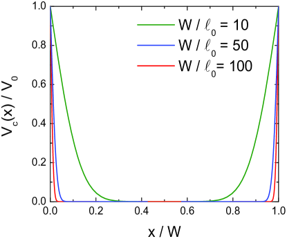
for a conducting channel of width with well depth . Here, is the complimentary error function. Plots of as a function of are shown in Fig. 2 for three values of . For this potential, the Hamiltonian (2) gives a term
| (6) |
where each Gaussian has width at the edges and . In Eq. (6), is related to the electric field due to lateral confinement in the direction. Since characterizes the steepness of the potentials at the two edges, we are at liberty to use a range of values of the ratio of these two lengths, keeping in mind that the in-plane confinement must be appreciable if the -term is to play a role. Therefore, in most of our calculations, we use only one small value of to illustrate the effects arising from our model on the conductance and thermoelectric power. We introduced the parameter , which is expressed in terms of fundamental constants as well as and . The is another Rashba parameter due to the electric confinement along the direction, and it is simply denoted as thereafter in this paper. Comparison of typical electric fields originating from the quantum well and lateral confining potentials allows one to conclude that a reasonable estimate moroz for should be roughly 10% of . The -SOI term in Eq. (6) is asymmetric about the mid-plane and varies quadratically with the displacement from either edge. In this quasi-square well potential, the electron wave functions slightly penetrate into the barrier regions. However, we only need energy levels for the calculations of ballistic transport electrons, not the wave functions, if we assume electronic system is a spatially-uniform quasi-one-dimensional one.
The eigenfunctions for the nanowire have the form
| (7) |
Since the nanowire is translationally invariant in the -direction with , where is a normalization length and , we must solve for and in Eq. (7) numerically due to the presence of edges at and . Substituting the wave function in Eq. (7) into the Schrödinger equation, i.e. with being the eigenenergy, we obtain the two coupled equations
| (8) |
In the absence of any edges, we may simply set for a quantum well, and get and , where and are independent of , and is the electron wave number along the direction, which then yields a pair of simultaneous algebraic equations for states and . But, in the case when there exist edges, we have a pair of coupled differential equations to solve for and which may be analyzed when only is not zero and then when both Rashba parameters are non-zero.
Two parameters of interest are
| (9) |
with three ratios
| (10) |
In our numerical calculations below, we will use three ratios to determine how sharp the nanowire potential is and how strong the Rashba parameters are.
II.1 Energy Bands for
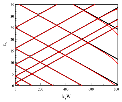
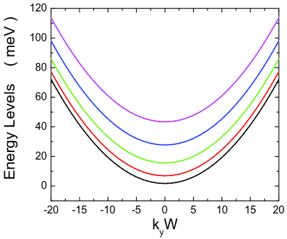
When we set in Eq. (8), and are equal to each other () and are solutions of a Schrödinger equation with a potential term present. When we solved the wave equations, we imposed the condition that the wave functions must vanish when either or holds. However, our calculations showed that the wave functions are negligible on the two edges of the nanowire when the confining potential is deep and sharp. The effect of the potential depends on , leading to a dependence of the transverse energy on the longitudinal wave number . If we set equal to zero in Eq. (8), the solutions are approximately those for a quasi-square well when is chosen small and the potential barriers are high (see Fig. 2). In this case, the transverse energy eigenvalues are approximately given by , where and . In Fig. 3, we present the energy bands for the calculated transverse energy in units of when the electric field-induced Rashba SOI parameter is set equal to zero so that only the effect from the -term is included. The two equations coincide and, of course, there is no effect from the Rashba term on when , and the eigenvalues are equal to those of the square well with high barriers corresponding to . However, as is increased, decreases linearly as a function of before its first drop. On the other hand, the dependence of the transverse energy has been shown to be a strong non-linear function of at its drop. As a matter of fact, the levels anti-cross at a value of which is determined by the chosen value of and .
The displacing effect of the -coupling on the eigenstates is reminiscent of the role played by magnetic field on the eigenenergies of a quasi-one-dimensional electron gas with harmonic confinement. However, the anti-crossing seems to be a unique property of the square barrier model with high potentials at the edges since it was not reported by Moroz and Barnes moroz for a parabolic confinement. Figure 3 shows that when , it does not matter what value is chosen because the energy level dependence on remains the same. When , the influence on the dispersion can be seen. However, this part of the energy spectrum makes a negligible contribution to the transport and thermoelectric power.
II.2 Energy Bands for
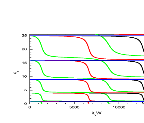
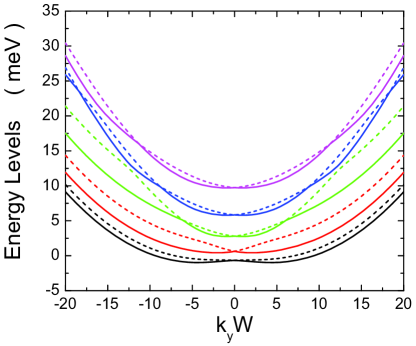
In Fig. 4, we present the transverse energies in units of as functions of for a non-zero value of . The plots compare the results for two chosen values of (black curve) and (red curve). The energy bands for the infinite 2DEG at due only to the -coupling (without transverse confinement) consist of a pair of spin-split upward-curved parabolic-like energy dispersions which are displaced in -space and degenerate at , and become split as increases. In the presence of edges for a nanowire, there is a discrete set of eigenstates for a chosen value of . These energy subbands then anti-cross. This anti-crossing effect increases as the value of is increased, as demonstrated by comparing the results of Fig. 4. These results are qualitatively in agreement with Fig. 3 in Ref. [moroz, ] (see also Ref. [gumbs1, ]) The difference is that for reasonable values of and , the scaled becomes larger in comparison with a parabolic confinement for one to see the anti-crossing behavior.
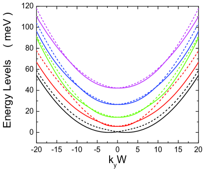
Figures 5 show plots of total energy levels with as functions of for , (upper-left panel) and , (upper-right panel), respectively. For the sake of comparison, the plot for , , and (lower panel) is also presented in this figure. From Figs. 5, we easily find that the energy dispersion is symmetric with respect to . Our results (two upper panels) further show that, as expected from Eq. (8), the -term has an effect when on the unperturbed energy eigenvalues in the absence of any Rashba SOI. As is increased, the SOI lifts the degeneracy of the energy subbands, as shown by a pair of solid and dashed curves degenerated at in the upper two panels. We further observed that when the -coupling is weak (upper-left panel), each branch of the energy curves, except for the first branch, has only one local minimum and this occurs at . As is increased (upper-right panel), two local minima develop symmetrically on either side of with a local maximum at for each branch.
III Model for Ballistic Charge Transport
In this section, we briefly outline our method of calculation for the ballistic conductance and electron-diffusion thermoelectric power. In our case, the energy bands are symmetric with respect to the wave numbers . For the symmetric bands, energy dispersion , the Fermi function , and the group velocity satisfy the relations: , , and . Therefore, one can write the following equation LYO:2004 in a form which includes only positive values of the wave number for the ballistic heat () and charge () currents, i.e.,
| (11) |
where , is the bias voltage between the source and drain electrodes, is the sign function, , and is the chemical potential. In Eq. (11), the whole energy integration performed over the range is divided into the sum of many sub-integrations between two successive extremum points for , and is the last minimum point. For each sub-integration over , is a monotonic function. In addition, each sub-integration in Eq. (11) can be calculated analytically, leading to the following expression for electron-diffusion thermoelectric power
| (12) |
where is the temperature, , and the dimensionless conductance is given by
| (13) |
Physically, the quantity defined in Eq. (13) represents the number of pairs of the Fermi points at K. In Eqs. (12) and (13), the summations over are for all the energy-extremum points on each th spin-split subband in the range . The quantity is the energy at the extremum point . For a given th spin-split subband, (or ) for a local energy minimum (maximum) point. The physical conductance is related to for spin-split subbands through
| (14) |
IV Numerical Results of Charge Transport
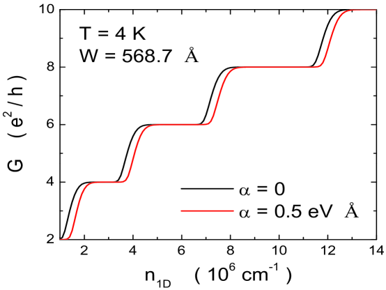
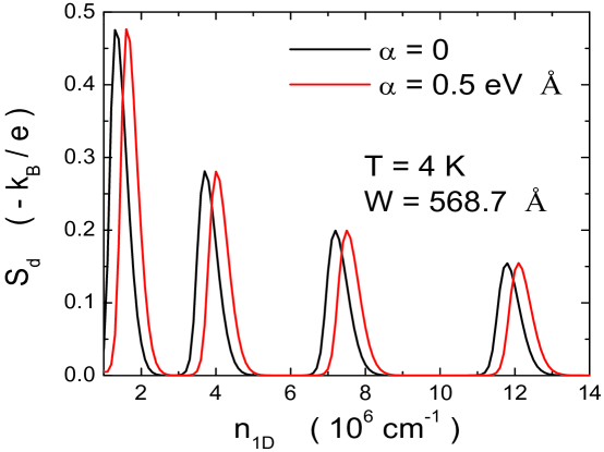
In Figs. 6, we have displayed comparisons of modified electron density () dependence of the ballistic conductance () and the electron-diffusion thermoelectric power () by the -term in the SOI when K and Å. From the upper panel of Fig. 6, we find that, as (black curve), a number of steps in show up as a result of successive populations of more and more spin-degenerate subbands, shown in the lower panel of Fig. 5. In addition, the observed plateau becomes wider and wider as higher and higher subbands are occupied by electrons due to increased energy-level separation, resulting from the high potential barriers at the two edges. The finite-temperature effect can easily be seen from the smoothed steps in this figure. As is increased to eVÅ (red curve), the steps are rightward shifted to higher electron densities due to an enhanced density-of-states from the flattened subband dispersion curves by SOI, as seen from the upper-left panel of Fig. 5. However, the step sharpness remains constant in this case. Furthermore, there exists no “pole-like feature” moroz in this figure, which can be traced back to the absence of spike-like feature in the subband dispersion curves, leading to additional local energy minimum/maximum points. The suppressed spike-like feature in the subband dispersion curves can be explained by a nonlinear dependence near the center () of a transverse symmetric potential well with a large value in our model for wide quantum wires, instead of a linear dependence close to the center of the confining potential in the model proposed by Moroz and Barnes moroz for narrow quantum wires. We also see sharp peaks in from the lower panel of Fig. 6 as (black curve), corresponding to the steps in , which again comes from successive population of spin-degenerate subbands with increased . huang1 The center of a plateau in aligns with the minimum of between two peaks. huang1 The peaks (red curve) are rightward shifted accordingly in electron density when a finite value of is assumed.
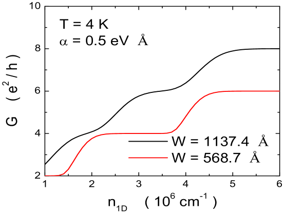
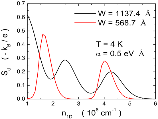
We have compared in Figs. 7 the results of and for two values of wire width at K and eVÅ. We find from the upper panel of Fig. 7 that, as decreases from Å (black curve) to Å (red curves), the steps in are leftward shifted in electron density, and meanwhile, the steps become sharpened. The step shifting is a result of the reduction of SOI effect due to a smaller value for (proportional to ) with a fixed value of , by comparing the upper-right panel with the upper-left panel of Fig. 5. This leads to a leftward shift in steps for the same reason given for the upper panel of Fig. 6. The step sharpening, on the other hand, comes from the significantly increased subband separation (proportional to ), which effectively suppresses the thermal-population effect on for smoothing out the conductance steps. The shifting of steps in with is also reflected in , as shown in the lower panel of Fig. 7. The peaks of get sharpened due to the suppression of in the density region corresponding to the widened plateaus of .
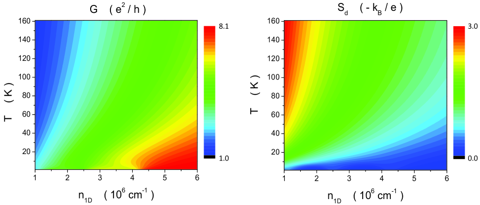
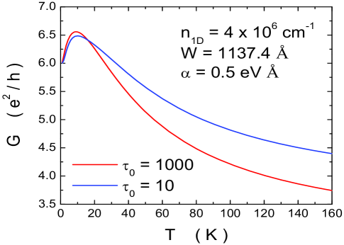
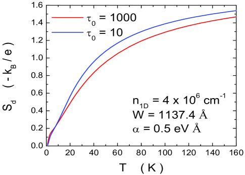
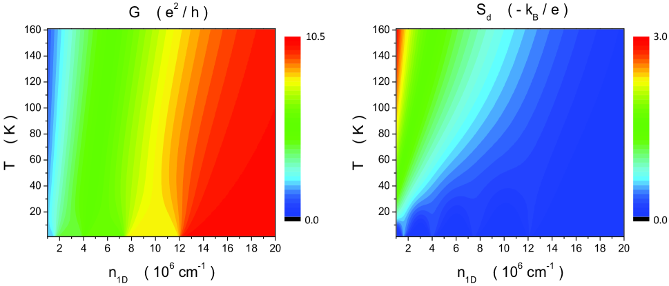
In order to achieve an overview for the variations of and with both and , we present two contour plots of these quantities, respectively, in Figs. 8 with Å and eVÅ. From the upper-left panel of Fig. 8, we find that decreases with , but increases with in general. The increase of with is a direct result of opening more conduction channels, i.e. more populated subbands, for ballistically-transported electrons. The reduction of with is a consequence of the dramatic decrease of the chemical potential with for a fixed (not shown), and then, the decrease of the Fermi function in Eq. (13) for K. However, does increase with at cm-1 within the range K, as shown in the lower-left panel of Fig. 8, because of the anomalous increase of the chemical potential with in this temperature range whenever the Fermi energy at K is set close to a minimum of any one of spin-split subbands. When is reduced from (red curve) to (blue curve) for softer potential edges, is only slightly decreased at low , but is significantly increased at high . We also find, from the upper-right panel of Fig. 8, that increases with but decreases with . The decrease of with is simply due to the increase of . As expected, varies linearly with for small values of but deviates from the linear behavior for large values of , as shown in the lower-right panel of Fig. 8. huang1 However, , in this case, goes towards its minimum value about zero at cm-1 as because approaches the quantized value for this electron density. When is reduced from (red curve) to (blue curve), is enhanced at high .
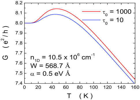
Finally, we show another pair of contour plots for and in Fig. 9 as functions of and with Å and eVÅ. Here, similar to the two upper panels of Fig. 8, (upper-left panel) increases with but with much steeper steps, and (upper-right panel) decreases with but at a more rapid rate at a higher temperature. At a higher electron density cm-1 in the lower-left panel of Fig. 9, for a reduced value of , the range for anomalous increase of with expands up to K. This is further accompanied by a locking of to its quantized value at for K. However, is reduced at high in this case when is reduced from (red curve) to (blue curve). Moreover, the locked value leads to an almost zero value for within this temperature range, as seen from the lower-right panel of Fig. 9. A clear linear dependence of on is found for K due to suppressed thermal-population effect by a reduced wire width. When is reduced from (red curve) to (blue curve), no significant changes to can be observed here.
V Concluding Remarks
In this paper we investigated the effect that the spin-orbit interaction has on the energy band structure, the conductance and the electron-diffusion thermoelectric power of a nanowire. We used a model in which edge effects for the nanowires are taken into account by solving numerically Dirac’s equation in a quasi-square potential. Comparing our model with the already published work where harmonic confinement was used to describe the transverse confinement, we found that the energy bands are different and in addition to crossing effect of the transverse energy bands, there is also anticrossing for specific finite values of . The -term of the Hamiltonian causes a displacement and a deformation of the transverse energy band structure which is more pronounced for large values of . The conductance plateaus become wider when the electron density is increased as a result of larger energy-level separation as the higher subbands are occupied by electrons. Also, due to the nonlinear dependence of -SOI on position close to the well center, there is no “pole-like feature” in which is obtained when a harmonic potential is assumed for confinement. The electron-diffusion thermoelectric power displays a peak whenever a spin-split subband is populated. At low temperature, the variation of is linear in but deviates from the linear behavior for large values of .
We note that if the effect due to electron interaction is strong in our system, the ballistic model in our paper cannot be justified. For high-mobility semiconductor quantum wires, electron transport is expected to be ballistic if the wire length is shorter than the mean free path of electrons in the system. On the other hand, electron transport can also be diffusive if the wire length is longer than the mean free path of electrons but less than the localization length. In the latter case, the interaction of electrons with impurities, roughness, phonons and other electrons will play a significant role in both the temperature and density dependence of electron mobility in quantum wires. For high temperature and low density, electron-phonon scattering is dominant. However, the electron-electron scattering becomes significant in a system with high density at low temperature. In this paper, we restricted ourselves to the ballistic regime for a short quantum wire.
Furthermore, In the absence of electron-electron interaction, an effect of lateral spin-orbit coupling on transport is to trigger a spontaneous but negligible spin polarization in the nanowire. However, the spin polarization is enhanced substantially when the effect of electron-electron interaction is included. The spin polarization may be strong enough to result in the appearance of a conductance plateau at a fractional value () of in the absence of any external magnetic field.pepper1 ; pepper2 ; thomas1 ; thomas2 The role played by electron-electron interaction on our results for the thermoelectric power in a nanowire may also be investigated using finite-temperature Green’s function techniques or field theoretic methods which would allow the classification of contributing diagrams.electron-electron This study should shed some light on whether electron-electron interaction enhances the thermoelectric power and how the SOI underlies the Peltier effect, i.e., the flow of entropy current in addition to the familiar charge current in an electric field. The effect of electron-electron interaction is expected to be significant at very low temperatures (less than 1K) and high electron densities. However, our model calculations are performed at temperatures at or higher than 4K.
Acknowledgements.
This research was supported by contract # FA 9453-07-C-0207 of AFRL. DH would like to thank the Air Force Office of Scientific Research (AFOSR) for its support.References
- (1) J. H. Davies, The Physics of Low-Dimensional Semiconductors, (Cambridge University Press, New York, 1998).
- (2) L. W. Smith, W. K. Hew, K. J. Thomas, M. Pepper, I. Farrer, D. Anderson, G. A. C. Jones, and D. A. Ritchie, Phys. Rev. B80, 041306 (2009).
- (3) W. K. Hew, K. J. Thomas, M. Pepper, I. Farrer, D. Anderson, G. A. C. Jones, and D. A. Ritchie, Phys. Rev. Lett. 102, 056804 (2009).
- (4) A. V. Moroz and C. H. W. Barnes, Phys. Rev. B60, 14272 (1999).
- (5) Y. V. Pershin, J. A. Nesteroff, and V. Privman, Phys. Rev. B69, 121306 (2004).
- (6) G. Gumbs, Phys. Rev. B70, 235314 (2004).
- (7) M. S. Kushwaha, Phys. Rev. B76, 245315 (2007).
- (8) G. Gumbs, Phys. Rev. B73, 165315 (2006).
- (9) G.-Q. Hai and M. R. S. Tavares, Phys. Rev. B61, 1704 (2000).
- (10) L. Brey and H. Fertig, Phys. Rev. B75, 125434 (2007).
- (11) C. G. Darwin, Proc. Roy. Soc. (London) 120, 621 (1928).
- (12) G. P. Fisher, Am. J. Phys. 39, 1528 (1971).
- (13) L. L. Foldy and S. A. Wouthuysen, Phys. Rev. 78, 29 (1950).
- (14) C. W. J. Beenakker and H. van Houten, Quantum Transport in Semiconductor Nanostructures, Vol. 44 of Solid State Physics (Academic Press, New York, 1991).
- (15) S. K. Lyo and D. H. Huang, J. Phys.: Condens. Matter, 16, 3379 (2004).
- (16) C. Itzykson and J.-B. Zuber, Quantum Field Theory (cGraw-Hill, New York, 1980).
- (17) V.K. Thankappan, Quantum Mechanics, (John Wiley and Sons, New York, 1993).
- (18) Yu. A. Bychkov and E. I. Rashba, J. Phys. C 17, 6039 (1984).
- (19) M. F. Li, Modern Semiconductor Quantum Physics, (World Scientific, Singapore, 1994).
- (20) B. K. Ridley, Quantum Processes in Semiconductors (Clarendon Press, Oxford, 1993).
- (21) T. Darnhofer and U. R ssler, Phys. Rev. B47, 16020 (1993).
- (22) S. K. Lyo and D. H. huang, Phys. Rev. B66, 155307 (2002).
- (23) K. J. Thomas, J. T. Nicholls, M. Y. Simmons, M. Pepper, D. R. Mace, and D. A. Ritchie, Phys. Rev. Lett. 77, 135 (1996).
- (24) K. J. Thomas, J. T. Nicholls, N. J. Appleyard, M. Y. Simmons, M. Pepper, D. R. Mace, W. R. Tribe, and D. A. Ritchie , Phys. Rev. B 58, 4846 (1998).
- (25) J. W. P. Hsu, A. Kapitulnik, and M. Yu. Reizer, Phys. Rev. B 40, 7513 (1989).