Temperature dependence of the nonlocal voltage in an Fe/GaAs electrical spin injection device
Abstract
The nonlocal spin resistance is measured as a function of temperature in a Fe/GaAs spin-injection device. For nonannealed samples that show minority-spin injection, the spin resistance is observed up to room temperature and decays exponentially with temperature at a rate of 0.018 K-1. Post-growth annealing at 440 K increases the spin signal at low temperatures, but the decay rate also increases to 0.030 K-1. From measurements of the diffusion constant and the spin lifetime in the GaAs channel, we conclude that sample annealing modifies the temperature dependence of the spin transfer efficiency at injection and detection contacts. Surprisingly, the spin transfer efficiency increases in samples that exhibit minority-spin injection.
The efficient injection of spin-polarized electrons from a ferromagnetic source into a semiconducting channel is a fundamental ingredient of spin-based electronic device concepts. The injected spin polarization can be detected by analyzing the degree of circular polarization of photons that are emitted in the semiconductor after recombination of the injected electrons with resident holes Alvarado and Renaud (1992); Ohno et al. (1999); Fiederling et al. (1999); Zhu et al. (2001); Hanbicki et al. (2002). In all-electrical devices, the concept of nonlocal spin detection Johnson and Silsbee (1985); Jedema et al. (2001); Lou et al. (2007); Ciorga et al. (2009); van ’t Erve et al. (2007); Appelbaum et al. (2007); Tombros et al. (2007) has been used to convert the injected spin polarization into a nonlocal voltage that is measured at a ferromagnetic detection contact to which the electron spins diffuse. This voltage depends not only on how efficient spins are injected and detected, but also on the loss of spin polarization during the diffusive spin transport in the semiconductor. For electrical spin-injection into GaAs, a rapid decay of with temperature has been reported Lou et al. (2007); Ciorga et al. (2009), in contrast to the measured circular polarization of electroluminescence that remains observable up to room temperature Zhu et al. (2001) and is strongly influenced by the interplay of spin lifetime and radiative recombination time Salis et al. (2005). For Fe on GaAs(001), the sign and magnitude of the measured spin injection depend delicately on the growth temperature of the Fe layer as well as on a post-growth annealing treatment, where a reversal from minority to majority spin injection has been observed Schultz et al. (2009). Post-growth annealing also has a strong influence on the magnetic properties of ferromagnetic thin films on III-V compounds Shaw and Falco (2007); Bianco et al. (2008).
Here we report a considerable change in the temperature dependence of the spin transfer efficiency across the ferromagnet/semiconductor interface that occurs after annealing Fe/GaAs samples at moderate temperature. We investigate the nonlocal spin resistance as a function of temperature up to 300 K ( is the current across the spin injection contact). We find an exponential decay of with from 5 to 200 K with a rate that depends strongly on the annealing conditions. After annealing the sample at 440 K, decays considerably faster with . In order to understand this dependence, we characterize the spin decay in the GaAs channel by measuring the spin lifetime and the diffusion constant in the channel. Since does not change after sample annealing, the strong modification with annealing must arise from a change in the -dependence of . By writing , where the spin-injection efficiency specifies the spin polarization of an electron that has just tunneled from the Fe injection contact into the GaAs channel, and describes the relation between the spin polarization below the detection contact and , we find the dependence of . For annealed samples, is almost independent on , whereas for those nonannealed samples that show minority-spin injection, rises with between 30 and 140 K. This unexpected result is discussed in terms of interface-related mechanisms that increasingly favor minority-spin transfer across the interface.
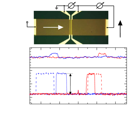
The samples under investigation consist of an n-doped GaAs spin transport layer as described in Ref. Salis et al. (2009) and Fe contacts for spin injection and detection. Four 56-m-long contact bars were defined by evaporating 5 nm Fe and 2 nm Au through a nanostencil mask Zahl et al. (2005), see Fig. 1(a). These bars are electrically contacted by 100-nm-thick TiAu that is insulated from GaAs by a 100-nm-thick Al2O3 layer. The middle bars (2 and 3) serving as spin injection and detection contacts are 1 and 3 m wide and separated by a gap of m. Between contacts 1 and 2, a bias is applied. For positive , spin-polarized electrons are injected at contact 2 into the spin transport channel and drift towards contact 1. For negative , electrons drift from contact 1 to contact 2 and spin polarization accumulates below contact 2 because of spin filtering Lou et al. (2007). In both cases, spin polarization diffuses towards contact 3, where a potential with respect to contact 4 is measured. By switching the alignment of the magnetizations of the injection and detection contacts from antiparallel to parallel with an external magnetic field , two values for are measured that differ by which is proportional to the average spin polarization below the detection contact. From measurements using a lock-in amplifier, we obtain , from which and were determined by integration over . The voltage drop across the Schottky barrier of contact 2 was measured as a potential difference between contacts 3 and 2. The highest temperature that the nonannealed samples have seen before measurement is 390 K.

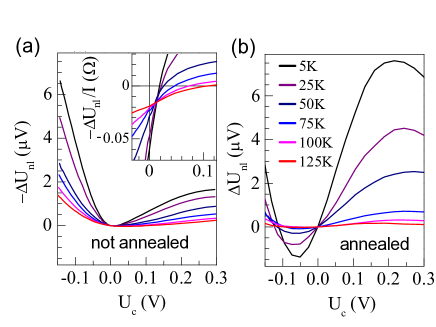
From data of versus [Fig. 1(b)] we determine . For nonannealed samples, decreases by a factor of 80 between 5 and 300 K. The values for versus are shown in Fig. 2 for between 5 and 125 K. We find a nonmonotonic dependence of on . It is helpful to consider that is proportional to the product of and the spin injection efficiency , such that . As can be seen from the inset of Fig. 2(a), in the nonannealed sample, changes sign for , i.e., for spin injection. Such behavior has been related to a transition from minority to majority spin injection with increasing Moser et al. (2006); Lou et al. (2007). In the annealed samples, reverses its sign at , see Fig. 2(b), and majority spins are injected at . Because of the opposite sign of spin injection close to zero bias, also has opposite signs Lou et al. (2007) for the the annealed and nonannealed sample. In Fig. 2, we therefore plot for the nonannealed sample. Although the dependence of on is not understood in detail, it has been related to the interfacial structure between Fe and GaAs Chantis et al. (2007); Schultz et al. (2009) or to a confinement layer in the semiconductor Dery and Sham (2007), which will be discussed later.

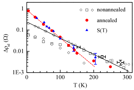
Figure 3 summarizes the -dependence of for both nonannealed and annealed samples. For the nonannealed sample, decays exponentially with increasing up to 200 K. The decay rate is about K-1 (black line) for both and 100 mV. For mV, a more complicated behavior with is observed, which we attribute to the crossing of at small positive , i.e. to the bias dependence of . Annealing the sample increases at low , but at the same time, decreases much faster with , namely, at a rate of 0.030 K-1 (red dashed line). This faster decrease results in a signal that at higher becomes smaller than that of the nonannealed sample. The data for the annealed sample were obtained at , but similar behavior is observed for mV (not shown).
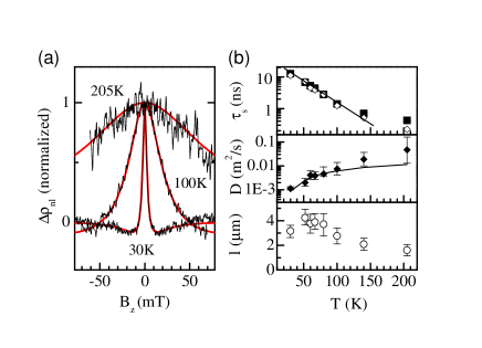
The magnitude of depends on and , as well as on the transport and spin dynamics in the GaAs channel that reduces the injected spin polarization to a value at the detection contact. is characterized by the diffusion constant and the spin lifetime , which are obtained from Hanle measurements at different , as shown in Fig. 4(a). When the spins in the channel precess about a perpendicular magnetic field , decreases because of the distribution in the arrival times of the injected spins at contact 3. This can be calculated by the one-dimensional Hanle integral Jedema et al. (2001)
| (1) |
where is the electron g-factor of GaAs, the Bohr magneton, Planck’s constant, and the distance between injection and detection of the spins. To account for the finite width of the detection contact, Eq. (1) is integrated for ranging from to . Because of the electric field applied between contacts 1 and 2, it is assumed that all spins are injected at the edge of contact 2 towards contact 3.
Two-parameter fits of the Hanle data with and as parameters are shown in Fig. 4(a), and the resulting fit parameters are summarized in Fig. 4(b). The error bar for arises from an uncertainty in an offset in , which becomes larger at higher , where the tails of the Hanle peak can no longer be measured. For K, the Hanle peak was normalized to the value of for an in-plane magnetic-field sweep. For K, the values of of the two-parameter Hanle fits match well the data of obtained from a four-point Hall measurement. For K, the Hanle fit values deviate towards higher values, which we attribute to the weak influence of on the Hanle curves at higher . We therefore also fit the data with as the only fit parameter and fix to the transport value. In Fig. 4(b), the results for are shown for both the one- and two-parameter Hanle fits. The two fits yield similar results, namely, a that decays approximately exponentially with from 12 ns at 30 K to 200 ps at 205 K. From and , the spin diffusion length is calculated. The combined increase of and decrease of lead to only a small decrease of , from 4 m at 50 K to 1.6 m at 200 K. In Ref. Ciorga et al., 2009, m was found at K, whereas Ref. Lou et al., 2007 measures m at 50 K, comparable to our values. It is important to note that post-growth annealing does not affect the spin transport properties of the GaAs channel, as verified in separate measurements on an annealed sample.

The contribution to can be calculated from Eq. (1) with . The integration over yields . decays exponentially with the separation between injection and the detection contact, and stems from the integration over time, where spins contribute in a time and spread over a length . The proportionality of to influences more strongly than the relatively weak variation of with does. as obtained not (a) from the one-parameter Hanle fits is shown in Fig. 3 as triangles, scaled by a factor for better comparison with . The overall -dependence of is determined from . Since the decay rate of of the annealed sample is very similar to that of , does not change much with in that sample. However, before annealing, decreases significantly less, amounting to a factor of 3.7 between 30 and 140 K. This suggests that increases with below 140 K. Above 140 K, the slope of is similar to that of for both the annealed and the nonannealed samples.
To ensure that Eq. (1) and thus does not overestimate the decay rate attributed to the GaAs channel, some care has to be taken. In fact, there are several limitations to Eq. (1). First, it is derived in the limit of small spin polarization in the GaAs channel by assuming that there the spin injection rate does not depend on the spin polarization in the GaAs channel. More generally, the spin injection rate is proportional to the difference between and the spin polarization in the GaAs channel. This modification is equivalent to adding an effective spin decay rate 1/, given by the rate of injected electrons divided by the number of electrons in the channel below the injection contact. For our sample geometry, we obtain ns for a typical current of A, which is comparable to the spin lifetime of 12 ns at 30 K. The result is that saturates with increasing . From a solution of the spin drift-diffusion equation, we find that the corresponding reduction of is smaller than 30% at 30 K. Second, Eq. (1) neglects the drift of spin polarization towards contact 1. This effect has an influence on that is smaller than 10% for A at mV and at 30 K. We can also neglect that dynamic nuclear polarization enhances the applied field Lou et al. (2006); Salis et al. (2009) at small , which would lead to overestimated values for . Such dynamic nuclear polarization sensitively depends on a misalignment between sample normal and , and we do not find large variations of the measured above 30 K.

Considering the limitations above, we estimate that the decay rate of between 30 and 140 K is at least 0.025 K-1, corresponding to a loss of spin polarization in the channel of a factor of at least 16 when is increased from 30 to 140 K. In this -range, however, measured in the nonannealed sample exhibits a much weaker decrease, namely, only by a factor of 7, whereas for the annealed sample the factor increases to 27. These strong, annealing-induced changes must be related to a modification of the spin injection or detection efficiency that occurs at the interface. They are concomitant with a shift from minority- to majority-spin injection. We recall that annealing at moderate is known to affect only the Fe/GaAs(001) interface region, giving rise to structural changes that lead to an enhanced crystal order Zega et al. (2006); Shaw and Falco (2007) and enhanced polarization injection efficiency Zega et al. (2006); Adelmann et al. (2005). The important result is that before moderate post-growth annealing, increases with increasing . Such an increase is likely to be related to a change in the weighting of minority- and majority-spin processes not (b). The spin-filter effect due to symmetry conservation of the coupling between the Fe and GaAs wave functions at the interface strongly favors majority spin injection Wunnicke et al. (2002) for the case of well-ordered Fe/GaAs interfaces. On the other hand, a resonant state arising from interface layers promotes minority-spin injection Chantis et al. (2007). In addition, the existence of a bound state in the semiconductor close to the interface can influence both the size and sign of accumulated spin polarization Dery and Sham (2007). The exact balance of minority and majority spin contributions is determined by the interplay of all these effects. The important question is how a change in redistributes the weight of the individual contributions. As is increased, the distribution of electrons that tunnel through the Schottky barrier extends towards higher energies at which the tunneling probability becomes significantly larger. This change in energy and a simultaneous modification of the in-plane electron momentum of the tunneling electrons may influence the resonance with the minority peak Chantis et al. (2007). An additional role could be played by a change in the overlap of GaAs and Fe wave-functions that determines the spin filtering efficiency, as well as by a -dependent variation of the occupation of a semiconductor bound state. The similar decay rate found for positive and negative in the nonannealed sample points to a positive -dependence of , induced by a shift towards the minority peak as is increased. This is strongly supported by the position of the zero-crossing of that occurs at higher when is increased [inset of Fig. 2(a)], which is compatible with the majority contribution moving farther away from and therefore the minority peak gaining in strength. This results in a positive -dependence of at and by reciprocity also of . Away from , only the increase in is seen in , whereas at , both and contribute, leading to an even slower decay of , in agreement with our data, see Fig. 3.
In conclusion, we observe a strong change in the temperature dependence of the nonlocal spin resistance upon post-growth sample annealing, which we relate to a change in the dependence of the spin-transfer efficiency at the injection and detection contacts. For annealed samples, the spin transfer efficiencies increase with up to 140 K. Such behavior is likely associated with an interplay of interface-related mechanisms that more and more favors the minority-spin as is increased.
We acknowledge valuable discussions with Rolf Allenspach, and technical support from Meinrad Tschudy, Daniele Caimi, Ute Drechsler and Martin Witzig.
References
- Alvarado and Renaud (1992) S. F. Alvarado and P. Renaud, Phys. Rev. Lett. 68, 1387 (1992).
- Ohno et al. (1999) Y. Ohno et al., Nature 402, 790 (1999).
- Fiederling et al. (1999) R. Fiederling et al., Nature 402, 787 (1999).
- Zhu et al. (2001) H. J. Zhu et al., Phys. Rev. Lett. 87, 016601 (2001).
- Hanbicki et al. (2002) A. T. Hanbicki et al., Appl. Phys. Lett. 80, 1240 (2002).
- Johnson and Silsbee (1985) M. Johnson and R. H. Silsbee, Phys. Rev. Lett. 55, 1790 (1985).
- Jedema et al. (2001) F. J. Jedema, A. T. Filip, and B. J. van Wees, Nature 410, 345 (2001).
- Lou et al. (2007) X. Lou et al., Nat. Phys. 3, 197 (2007).
- Ciorga et al. (2009) M. Ciorga et al., Phys. Rev. B 79, 165321 (2009).
- van ’t Erve et al. (2007) O. M. J. van ’t Erve et al., Appl. Phys. Lett. 91, 212109 (2007).
- Appelbaum et al. (2007) I. Appelbaum, B. Huang, and D. J. Monsma, Nature 447, 295 (2007).
- Tombros et al. (2007) N. Tombros et al., Nature 448, 571 (2007).
- Salis et al. (2005) G. Salis et al., Appl. Phys. Lett. 87, 262503 (2005).
- Schultz et al. (2009) B. D. Schultz et al., Phys. Rev. B 80, 201309(R) (2009).
- Shaw and Falco (2007) J. M. Shaw and C. M. Falco, J. Appl. Phys. 101, 033905 (2007).
- Bianco et al. (2008) F. Bianco et al., J. Appl. Phys. 104 (2008).
- Salis et al. (2009) G. Salis, A. Fuhrer, and S. F. Alvarado, Phys. Rev. B 80, 115332 (2009).
- Zahl et al. (2005) P. Zahl et al., Rev. Sci. Instr. 76, 023707 (2005).
- Moser et al. (2006) J. Moser et al., Appl. Phys. Lett. 89, 162106 (2006).
- Chantis et al. (2007) A. N. Chantis et al., Phys. Rev. Lett. 99, 196603 (2007).
- Dery and Sham (2007) H. Dery and L. J. Sham, Phys. Rev. Lett. 98, 046602 (2007).
- not (a) For calculation of , an additional integration over the width of the detection contact did not change the slope of .
- Lou et al. (2006) X. Lou et al., Phys. Rev. Lett. 96, 176603 (2006).
- Zega et al. (2006) T. J. Zega et al., Phys. Rev. Lett. 96, 196101 (2006).
- Adelmann et al. (2005) C. Adelmann et al., Phys. Rev. B 71, 121301(R) (2005).
- not (b) Irrespective of sample annealing, also depends on the density-of-states in GaAs at the Fermi energy and thus on carrier density. In the measured range, we observe only a small increase of the carrier density, from 5 to 6 cm-3.
- Wunnicke et al. (2002) O. Wunnicke et al., Phys. Rev. B 65, 241306(R) (2002).