Thin-Film Metamaterials called Sculptured Thin Films
Akhlesh Lakhtakia1 and Joseph B. Geddes III2
1Department of Engineering Science and Mechanics, Pennsylvania State University, University Park, PA 16802, USA
2Beckman Institute, University of Illinois at Urbana–Champaign, Urbana, IL 61801, USA
Abstract
Morphology and performance are conjointed attributes of metamaterials, of which sculptured thin films (STFs) are examples. STFs are assemblies of nanowires that can be fabricated from many different materials, typicially via physical vapor deposition onto rotating substrates. The curvilinear–nanowire morphology of STFs is determined by the substrate motions during fabrication. The optical properties, especially, can be tailored by varying the morphology of STFs. In many cases prototype devices have been fabricated for various optical, thermal, chemical, and biological applications.
1 Introduction
The emergence of metamaterials at the end of the 20th century heralded a major motivational shift in research on materials and coincided with the ramping up of nanotechnology [1]. Materials researchers began to consider the design of composite materials, called metamaterials, to perform more than role each in specific environments. Among optics researchers today, the term metamaterial is often taken to mean a material with negative refractive index [2], but there is much more to metamaterials than that. In the year 2000, Rodger Walser [3] coined this term for certain types of artificial materials, and later formally defined metamaterials as “macroscopic composites having a manmade, three-dimensional, periodic cellular architecture designed to produce an optimized combination, not available in nature, of two or more responses [emphasis in the original] to specific excitation. We can relax the requirements of periodicity today, though not of cellularity. Indeed, cellularity in morphology engenders multifunctional performance.
Sculptured thin films (STFs) [4] exemplify metamaterials. An STF is an assembly of nanowires typically grown by physical vapor deposition, whose bent and twisted forms are engineeered via the growth process. As a result of the flexibility in controlling the evolving nanostructure of the films during fabrication, their performance characteristics can be engineered.
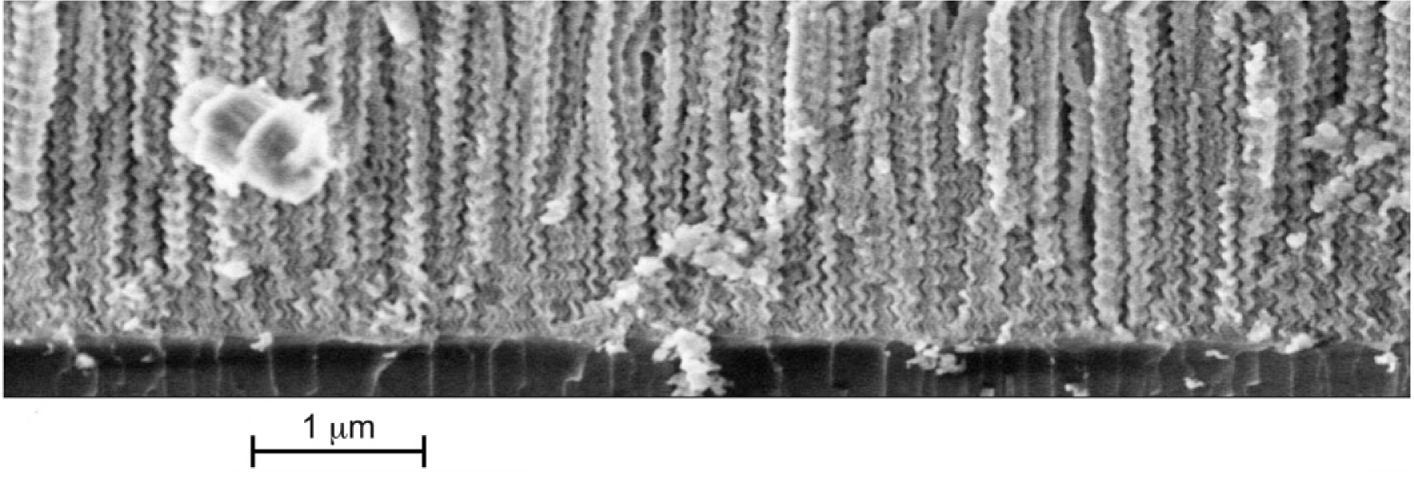
The curvilinear–nanowire morphology of STFs is exemplified by Fig. 1. Note the individual nanowires that make up the STF in this case are helical; they are also nominally identical and parallel. The constituent nanowires of an STF have diameters of 10–300 nm, and lengths on the order of tens of nanometers to several micrometers. The nanowires are made of clusters 1–3 nm in linear dimension. Therefore, STFs may be classified as nanomaterials. For many applications dependent on optical or infrared radiation, the closely packed nanowires can be treated effectively as equivalent to an anisotropic and nonhomogeneous continuum.
Possibly the first STF was fabricated by Young and Kowal in 1959 [5], who made fluorite films via oblique evaporation onto a rotating substrate. Although the structure of the resulting film was not unambiguously determined, the film did display optical activity. Most likely, the film was structurally chiral, as in Fig. 1. This development was preceded by about 75 years of growing columnar thin films by thermal evaporation [6]. Columnar thin films are assemblies of parallel straight nanowires, and are optically akin to biaxial crystals. The emergence of scanning electron microscopy in the late 1950s and early 1960s led to the confirmation of nanowire morphology. In 1966, a significant event occurred when Nieuwenhuizen and Haanstra showed that the nanowire inclination could be altered within a transitional distance of about 30 nm [7].
Messier and colleagues identified the conditions for the emergence of the nanowire morphology [8]. In 1989, Motohira and Taga showed that the direction of growing nanowires could be altered often within a few nanometers by appropriately switching the direction of the incoming vapor mid-deposition [9]. Lakhtakia and Messier realized that nanowires with almost arbitrary shapes could be fashioned by continuously changing the direction of the incoming vapor during deposition [10]. Robbie and colleagues reported the first STF with unambiguously determined structure [11]. Since that time, hundreds of research papers, a monograph [4], and many book chapters have been written on STFs [12, 13, 14, 15, 16].
This article contains a brief description of and the physical phenomenons exhibited by STFs. In many cases, those phenomenons are due directly to the symmetries that the structures of the constituent nanowires break. In Section 2, we review the fabrication of STFs. Then in Section 3, we present the mathematical description of the optical constitutive relations of STFs. In Section 4, we review the optical, thermal, chemical, and biological applications to which STFs either have been put or have been suggested. The advantages and disadvantages of STF technologies compared to other technologies are presented in the same section. We end in Section 5 with some remarks on the extension of the STF concept for acoustic applications.
2 Fabrication of STFs
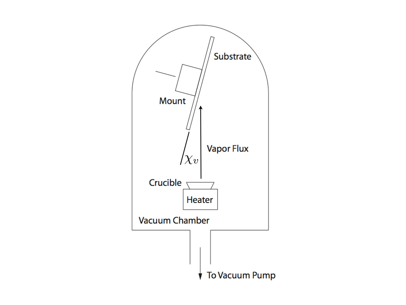
STFs are chiefly fabricated by physical vapor deposition [17]. Several variants exist, of which thermal evaporation is the simplest. A source material is evaporated under high vacuum and the vapor allowed to flow at an oblique incidence angle onto a substrate, as schematically depicted in Fig. 2. When the temperature of the source material is less than approximately one–third the melting temperature, there is little surface diffusion, and straight nanowires form. The morphology is enabled by the shadowing of nanowires by those in front of them.
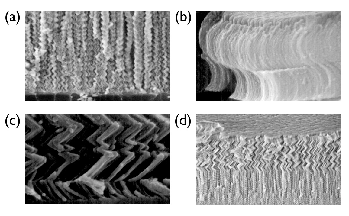
The nanowire morphology can be changed during deposition by tilting and rotating the substrate. When the substrate is rotated about a direction perpendicular to the substrate and passing through it, the nanowires become helical. These structures form the basis of chiral STFs, also known as thin–film helicoidal bianisotropic mediums (TFHBMs) in optical parlance. Several scanning electron micrographs of STFs, including TFHBMs, are shown in Fig. 3.
In addition, the substrate can be rotated about an axis in the plane of the substrate. Changing the tilt along either or both of two such orthogonal axes can lead to zigzag, c–, and s–shaped nanowires. Such STFs are known as sculptured nematic thin films (SNTFs). Several scanning electron micrographs of SNTFs are shown in Fig. 3.
Hybrid STFs that consist of both TFHBM and SNTF sections grown one after another are also possible. For example, Suzuki and Taga fabricated hybrid STFs with zigzag, helicoidal, and straight nanowire sections [18]. More recently, Park et al. grew a hybrid STF comprising three different chiral sections [19].
Several variations on the basic scheme are possible, including serial bideposition, multideposition, prepatterning of substrates, and hybrid chemical/physical vapor deposition. In serial bideposition, a single source is used to fabricate films with large local birefringence [20, 21]. For example, when growing chiral STFs, the source is manipulated to deposit alternately on either side of the growing nanowires. Multideposition consists of two or more sources being simultaneously evaporated to grow STFs [22]. Hybrid chemical/physical vapor deposition has been used to fabricate polymeric STFs [23, 24], because such materials cannot be heated to produce a collimated vapor.
Table 1. Materials from which STFs have been fabricated. Note that the list includes oxides, fluorides, metals, semiconductors, and polymers. Materials marked with ∗ indicate inverse structures formed by infilling of STF voids with the indicated material and subsequent removal of the initial STF. Material(s) Reference(s) Material(s) Reference(s) iron oxide [25] silicon oxide [17, 26, 27, 28] tantalum oxide [29] tin oxide [27] titanium oxide [21, 29, 30] zirconium oxide [29, 31] calcium fluoride [11, 26] magnesium fluoride [11, 17, 26] indium nitride [32] aluminum [27] chromium [26, 27] copper [26] gold [33]∗ manganese [26, 34] molybdenum [27] nickel [33]∗ carbon [35] silicon [36, 37, 38] GeSbSe chalcogenide [39, 40, 41] Alq3 [42] parylene [23, 24] polystyrene [33]∗
Inverse structures can be formed by infilling of STF voids via electrodeposition of metal or infiltration of molten polyer, and subsequent removal of the initial STF via etching [33].
STFs can be fabricated from just about any material that can be evaporated. A wide variety of materials, including dielectrics, metals, and polymers have been used to fabricate STFs. Table 1 lists several materials from which STFs have been fabricated. GeSbSe chalcogenide glasses and luminescent Alq3 have been used most recently [39, 40, 41, 42].
The structures into which STFs can be formed has also expanded to include three–dimensional STF architectures. STFs can be deposited on substrates that have been prepatterned via lithography or other processes. The STF nanowires grow on the raised areas (and, depending on the angle of incidence of the vapor, the side walls) to form three–dimensional structures [27, 28]. Alternatively, the pre–deposition of arrays of small islands, or seeds, of source material can result, after STF deposition, in patterns of single nanowires or clusters of nanowires [43, 44, 45].
3 Optical Constitutive Relations of STFs
Consider an STF that occupies the region . We use the cartesian coordinate system with the triad of unit vectors . The frequency-domain constitutive relations of such a dielectric, spatially local STF within this region are as follows:
| (1) | |||||
| (2) |
where and are the macroscopic primitive electric and magnetic field phasors; and are the corresponding induction field phasors; and are the permittivity and permeability of vacuum, respectively; is the angular frequency; and is the relative permittivity dyadic. The latter can be factored into pieces which depend either only on the structure of the film or the dispersive properties; thus,
| (3) |
where is the reference permittivity dyadic, so named to correspond to a reference plane where the rotation dyadic equals the identity dyadic (i.e., ).
There are two canonical forms for the rotation dyadic. When
| (4) |
the STF exhibits an essentially two–dimensional morphology (in the plane), and hence is called an SNTF. The angle determines whether the nanowires are chevrons, c–shaped, s–shaped, or of other more complex shapes.
When
| (5) |
the STF exhibits a three–dimensional morphology, and hence is called a TFHBM. Such films are structurally chiral. Often such STFs are formed with and are therefore periodic, where is the structural half–period. These periodically nonhomogeneous STFs are called chiral STFs.
In more complicated STFs, can be some combination of and . In hybrid STFs, both and can have sectionwise variations along the axis.
A link between the microscopic structure of an STF and its macroscopic constitutive properties is found by local homogenization in a nominal model of STF morphology [46]. This nominal model considers each STF nanowire as being composed of a string of homogenous ellipsoids; the voids are also treated as conglomerates of ellipsoids. Local homogenization of this model, for example with the Bruggeman formalism, yields . An extended model shows how STFs infiltrated with a chiral fluid could exhibit bianisotropic optical properties [47, 48].
4 Applications of STFs
A variety of the optical, electronic, chemical, and biological applications of STFs have been proposed and demonstrated.
4.1 Optical
The area of application for which STFs have been developed the most thoroughly is optics. The nanometer–scale control over the structure of STFs has meant that the optical properties of the films could be controlled on subwavelength scales. The recent development of three–dimensional STF architectures means that simultaneous control at both wavelength and subwavelength scales is possible—as in three–dimensional photonic crystals.
Even within the optics category, the most well–developed area is filter technology, particularly that relying on the circular Bragg phenomenon exhibited by chiral STFs. The chirality and periodicity of the latter can give rise to a stop band along the thickness direction. That is, left/right circularly polarized light over a bandwidth called the Bragg regime is mostly reflected by a sufficiently thick chiral STF that is structurally left/right handed, but right/left circularly polarized light is either transmitted or absorbed. In a more abstract sense, the chiral STF breaks both rotational and translational symmetries, and this gives rise to the circular Bragg phenomenon.
Due to their controllable void fraction, STFs have been suggested as low–permittivity dielectrics to reduce crosstalk in integrated circuits [49]. Also, efforts have begun to integrate active light emission and gain elements into STFs for optoelectronic applications. For example, a layer of optically pumped quantum dots was embedded between two chiral STF layers to create a device which emitted circularly polarized light [50]. Chiral STFs were also used to create a circularly polarized external–cavity diode laser [51]. In addition, the possibility of tunable polymeric chiral STF lasers, whose microstructure can be compressed and released by a piezoelectric element to control the output wavelength, has been analyzed [52]. A similar scheme has been suggested for tunable optical filters [53].
Another route to tunability is to infiltrate the pores of, for example, chiral STFs with liquid crystals. The aciculate molecules of the liquid crystal tend to align with the STF nanowires; this effect has been shown to increase the optical rotary power of the resulting composite films [54]. Moreover, one can apply an electric field to align the liquid crystal molecules along the field, with a concomitant change in optical properties for the composite [55].
A third route to tunability is to fabricate STFs from electro–optic materials [22, 56, 57]. Most notably, the chiral STFs exhibiting the Pockels effect can exhibit a Bragg regime in the presence of a low–frequency electric field [58].
A major emerging area in optics is to exploit STFs for plasmonics–based sensing of chemical and biological materials. For example, ultrathin metal STFs have shown a sensitivity that is significantly larger than for bulk films: /RIU for metal STFs in contrast to /RIU for bulk films [59]. Most recently, the propagation of multiple surface–plasmon–polariton waves, of the same frequency but different phase speeds, guided by a planar metal/STF interface has been theoretically predicted [60, 61, 62, 63] and experimentally verified [64], with exciting prospects for multianalyte sensing and error–free sensing.
Regardless of the excellence of optical performance characteristics, no STF can be used reliably if it cannot withstand mechanical stimuli within reasonable ranges. Various mechanical properties of STFs, such as hardness, compliances, yield stress, and ultimate strength, need to be modeled and measured in relation to STF morphology and composition. Furthermore, there is no experimental evidence showing how the optical properties change with the application of stress. This is practically virgin territory for research. It is known from indentation experiments that chiral STFs are permanently deformed when applied pressures exceed 30 Pa [65]. This problem could be alleviated by impregnating an STF with a polymer [33, 49] which shall have to be accounted for during optical design; however, that step will require experimentation. Moreover, polymer infiltration would allow STFs to be used as optical pressure sensors [4] as well as further the development of mechanically tunable light emitters and optical filters [52, 53].
4.2 Thermal
Harris et al. deposited alternating layers of solid and porous SNTFs of yttria–stabilized zirconia [31]. They found that the composite structure had a reduced thermal diffussivity compared to bulk films, with the added benefit of providing stress relief from expansion. The particular form of the SNTF structure they used was required to prevent cracking in the films.
4.3 Chemical
A variety of photochemical, electrochemical, and fluid sensor applications of STFs have also begun to be investigated.
Titanium dioxide STFs have been integrated into Grätzel cells for solar–power applications [66]. The photocatalytic properties of titanium–dioxide STFs have been found to depend on their morphology [18].
The porous structure of indium–nitride SNTFs and TFHBMs was shown to improve their electrochromic properties [32]. In addition, Brett and colleagues measured the electrohemical properties of carbon TFHBMs and chevronic manganese SNTFs [34, 35].
The porosity of STFs means that chemicals can infiltrate their pores and change their optical and electrical properties. For example, by depositing titanium–dioxide STFs on coplanar interdigitated electrodes, sensors whose capacitance increases with increasing relative humidity can be made [67]. Both the optical rotation and location of spectral hole within the circular Bragg phenomenon of a chiral STF also respond to the relative humidity of the environment [68, 69]. Shifts in spectrums have also been observed on complete infiltration of the voids in chiral STFs by acetone, methyl alcohol, isopropyl alcohol, and hexamethyldisilizane [66]. This experimental work was anticipated by earlier theoretical studies of both SNTFs and TFHBMs as fluid sensors [70, 71, 72]. The susceptibility of the optical properties of STFs to ambient moisture underscores the need for the proper packaging of films not intended for use as sensors.
4.4 Biological
These chemical applications are quickly being joined by biological ones. Magnesium–alloy STF coatings on stents are being fabricated to be bioabsorbable [66]. Parylene STFs have been fabricated as scaffolds on which, for example, both kidney and fibroblast cells can grow [22, 76]. STFs are particularly suited to serve as scaffolds because their structure effectively mimics that of a tissue’s extracellular matrix [22]. The ability to make transparent STFs means that cell cultures grown within them can be imaged, for example with confocal microscopy [22]. The degradation of iron(III) oxide STFs by metal–reducing bacteria has been shown to affect their optical properties, a result that indicates the possibility of using STF-based fiber optic sensors to measure bacterial activity below ground [25].
4.5 Advantages and Disadvantages
STF technology presents several advantages as compared with competing technologies. The fabrication process of STFs is very simple and cheap, especially as compared to conventional semiconductor patterning technologies. The fabrication process affords a high degree of control over STF morphology, and consequently properties. STFs can be made of many different kinds of materials. However, there are disadvantages too. STFs can be fragile, and so must be suitably packaged to prevent damage. Suitable packaging is also needed to prevent absorption of moisture and concomitant change in properties, unless the films are being used as sensors.
Thus STFs are probably most appropriate for applications where a high degree of control over film properties and cost are important, but mechanical stability is of lesser concern.
5 Concluding Remarks
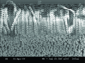
Extension of the STF concept for acoustic purposes requires a different length scale than that for optical purposes: nanometers have to be replaced by micrometers. Very recently, polymer STFs have been made on the microscale by a hybrid vapor deposition process; one such STF is shown in Fig. 4. Such films can be used as acoustic filters, both for polarization and bandwidth [77, 78, 79, 80, 81]. These films could also be used as MEMS elements, particularly for sensing. The acoustic properties of these STFs require experimental research coupled with theoretical modeling [82, 83, 84].
To conclude, STFs show promise for several optical, electronic, chemical, biological, and acoustic applications. Of these, the optical applications are the most developed. The controllable morphology and wide variety of constituent materials makes these thin-film metamaterials attractive for these and other applications.
Acknowledgments: J. B. Geddes III gratefully acknowledges support of a Beckman Postdoctoral Fellowship. A. Lakhtakia thanks the Binder Endowment at Penn State for financial support of his research.
References
- [1] A. Lakhtakia and T. G. Mackay. Meet the metamaterials. OSA Opt. Photon. News, 18(1):32–37, 2007.
- [2] T. G. Mackay and A. Lakhtakia. Negative refraction, negative phase velocity, and counterposition in bianisotropic materials and metamaterials. Phys. Rev. B, 79:235121, 2009.
- [3] R. Walser. Metamaterials: An introduction. In W. S. Weiglhofer and A. Lakhtakia, editors, Introduction to Complex Mediums for Optics and Electromagnetics, pages 295–316. SPIE Press, Bellingham, WA, USA, 2003.
- [4] A. Lakhtakia and R. Messier. Sculptured Thin Films: Nanoengineered Morphology and Optics. SPIE Press, Bellingham, WA, USA, 2005.
- [5] N. O. Young and J. Kowal. Optically active fluorite films. Nature, 183:104–105, 1959.
- [6] R. Messier. The nano–world of thin films. J. Nanophoton., 2:021995, 2008.
- [7] J. M. Nieuwenhuizen and H. B. Haanstra. Microfractography of thin films. Phillips Tech. Rev., 27:87–91, 1966.
- [8] R. Messier, A. P. Giri, and R. A. Roy. Revised structure zone model for thin film physical structure. J. Vac. Sci. Technol. A, 2:500–503, 1984.
- [9] T. Motohiro and Y. Taga. Thin film retardation plate by oblique deposition. Appl. Opt., 28:2466–2482, 1989.
- [10] A. Lakhtakia and R. Messier. The key to a thin film HBM: The Motohiro–Taga interface. In F. Mariotte and J.-P. Parneix, editors, Proceedings of Chiral ‘94; 3rd International Workshop on Chiral, Bi-isotropic and Bi-anisotropic Media, pages 125–130, Périgueux, France, 1994.
- [11] K. Robbie, M. J. Brett, and A. Lakhtakia. First thin–film realization of a helicoidal bianisotropic medium. J. Vac. Sci. Technol. A, 13:2991–2993, 1995.
- [12] V. C. Venugopal and A. Lakhtakia. Sculptured thin films: Conception, optical properties and applications. In O. N. Singh and A. Lakhtakia, editors, Electromagnetic Fields in Unconventional Materials and Structures, pages 151–216. Wiley, New York, NY, USA, 2000.
- [13] A. Lakhtakia and R. Messier. The past, the present, and the future of sculptured thin films. In W. S. Weiglhofer and A. Lakhtakia, editors, Introduction to Complex Mediums for Optics and Electromagnetics, pages 447–478. SPIE Press, Bellingham, WA, USA, 2003.
- [14] J. B. Geddes III. Towards shaping of pulsed plane waves in the time domain via chiral sculptured thin films. In P. K. Choudhury and O. N. Singh, editors, Frontiers in Optical Technology: Materials and Devices, pages 1–21. Nova Science, Hauppauge, NY, USA, 2006.
- [15] J. A. Polo. Sculptured thin films. In N. P. Mahalik, editor, Micromanufacturing and Nanotechnology, pages 357–381. Springer-Verlag, Berlin, Germany, 2006.
- [16] F. Wang. Optics of slanted chiral STFs. In D. L. Andrews and Z. Gaburro, editors, Frontiers in Surface Nanophotonics: Principles and Applications, pages 129–167. Springer, New York, NY, USA, 2007.
- [17] R. Messier, V. C. Venugopal, and P. D. Sunal. Origin and evolution of sculptured thin films. J. Vac. Sci. Technol. A, 18:1538–1545, 2000.
- [18] M. Suzuki and Y. Taga. Integrated sculptured thin films. Jap. J. Appl. Phys. Part 2, 40:L358–L359, 2001.
- [19] Y. J. Park, K. M. A. Sobahan, and C. K. Hwangbo. Wideband circular polarization reflector fabricated by glancing angle deposition. Opt. Exp., 16:5186–5192, 2008.
- [20] I. J. Hodgkinson and Q. H. Wu. Serial bideposition of anisotropic thin films with enhanced linear birefringence. Appl. Opt., 38:3621–3625, 1999.
- [21] I. J. Hodgkinson, Q. h. Wu, B. Knight, A. Lakhtakia, and K. Robbie. Vacuum deposition of chiral sculptured thin films with high optical activity. Appl. Opt., 39:642–649, 2000.
- [22] A. Lakhtakia, M. C. Demirel, M. W. Horn, and J. Xu. Six emerging directions in sculptured–thin–film research. Adv. Solid State Phys., 46:295–307, 2008.
- [23] S. Pursel, M. W. Horn, M. C. Demirel, and A. Lakhtakia. Growth of sculptured polymer submicronwire assemblies by vapor deposition. Polymer, 46:9544–9548, 2005.
- [24] M. C. Demirel, S. Boduroglu, M. Cetinkaya, and A. Lakhtakia. Spatially organized free–standing poly(p–xylylene) nanowires fabricated by vapor deposition. Langmuir, 23:5861–5863, 2007.
- [25] H. Tan, O. K. Ezekoye, J. van der Schalie, M. W. Horn, A. Lakhtakia, J. Xu, and W. D. Burgos. Biological reduction of nanoengineered iron(III) oxide sculptured thin films. Environ. Sci. Technol., 40:5490–5495, 2006.
- [26] K. Robbie, M. J. Brett, and A. Lakhtakia. Chiral sculptured thin films. Nature, 384:616, 1996.
- [27] M. W. Horn, M. D. Pickett, R. Messier, and A. Lakhtakia. Blending of nanoscale and microscale in uniform large–area sculptured thin–film architectures. Nanotechnology, 15:303–310, 2004.
- [28] M. W. Horn, M. D. Pickett, R. Messier, and A. Lakhtakia. Selective growth of sculptured nanowires on microlithographic lattices. J. Vac. Sci. Technol. B, 22:3426–3430, 2004.
- [29] I. Hodgkinson, Q. h. Wu, and J. Hazel. Empirical equations for the principal refractive indices and column angle of obliquely deposited films of tantalum oxide, titanium oxide, and zirconium oxide. Appl. Opt., 37:2653–2659, 1998.
- [30] A. C. van Popta, J. C. Sit, and M. J. Brett. Optical properties of porous helical thin films. Appl. Opt., 43:3632–3639, 2004.
- [31] K. D. Harris, D. Vick, E. J. Gonzalez, T. Smy, K. Robbie, and M. J. Brett. Porous thin films for thermal barrier coatings. Surf. Coat. Technol., 138:185–191, 2001.
- [32] Y. Inoue, A. Yamaguchi, T. Fujihara, J. Yamazaki, and O. Takai. Biomimetic improvement of electrochromic properties of indium nitride. J. Electrochem. Soc., 154:J212–J216, 2007.
- [33] A. L. Elias, K. D. Harris, and M. J. Brett. Fabrication of helically perforated gold, nickel, and polystyrene thin films. J. MEMS, 13:808–813, 2004.
- [34] J. N. Broughton and M. J. Brett. Electrochemical capacitance in manganese thin films with chevron microstructure. Electrochem. Solid–State Lett., 5:A279–A282, 2002.
- [35] G. K. Kiema and M. J. Brett. Electrochemical characterization of carbon films with porous microstructures. J. Electrochem. Soc., 150:E342–E347, 2003.
- [36] E. Schubert, J. Fahlteich, B. Rauschenbach, M. Schubert, M. Lorenz, M. Grundmann, and G. Wagner. Recrystallization behavior in chiral sculptured thin films from silicon. J. Appl. Phys., 100:016107, 2006.
- [37] D.-X. Ye, T. Karabacak, R. C. Picu, G.-C. Wang, and T.-M. Lu. Uniform Si nanostructures grown by oblique angle deposition with substrate swing rotation. Nanotechnology, 16:1717–1723, 2005.
- [38] D.-X. Ye, Z.-P. Yang, A. S. P. Chang, J. Bur, S. Y. Lin, T.-M. Lu, R. Z. Wang, and S. John. Experimental realization of a well–controlled 3D silicon spiral photonic crystal. J. Phys. D: Appl. Phys., 40:2624–2628, 2007.
- [39] R. J. Martín-Palma, J. V. Ryan, and C. G. Pantano. Surface microstructure of gesbse chalcogenide thin films grown at oblique angle. J. Appl. Phys., 101:083513, 2007.
- [40] R. J. Martín-Palma, J. V. Ryan, and C. G. Pantano. Spectral behavior of the optical constants in the visible/near infrared of gesbse chalcogenide thin films grown at glancing angle. J. Vac. Sci. Technol. A, 25:587–591, 2007.
- [41] R. J. Martín-Palma, A. Redondo-Cubero, R. Gago, J. V. Ryan, and C. G. Pantano. Rutherford backscattering spectrometry characterization of nanoporous chalcogenide thin films grown at oblique angles. J. Anal. At. Spectrom., 23:981–984, 2008.
- [42] P. C. P. Hrudey, K. L. Westra, and M. J. Brett. Highly ordered organic Alq3 chiral luminescent thin films fabricated by glancing–angle deposition. Adv. Mater., 18:224–228, 2006.
- [43] M. Malac, R. F. Egerton, M. J. Brett, and B. Dick. Fabrication of submicrometer regular arrays of pillars and helices. J. Vac. Sci. Technol. B, 17:2671–2674, 1999.
- [44] B. Dick, M. J. Brett, and T. Smy. Controlled growth of periodic pillars by glancing angle deposition. J. Vac. Sci. Technol. B, 21:23–28, 2003.
- [45] M. O. Jensen and M. J. Brett. Periodically structured glancing angle deposition thin films. IEEE Trans. Nanotechnol., 4:269–277, 2005.
- [46] J. A. Sherwin and A. Lakhtakia. Nominal model for structure–property relations of chiral dielectric sculptured thin films. Math. Comput. Modelling, 34:1499–1514, 2001. Corrections: 35:1355–1363, 2002.
- [47] J. A. Sherwin and A. Lakhtakia. Nominal model for the optical response of a chiral sculptured thin film infiltrated by an isotropic chiral fluid. Opt. Commun., 214:231–245, 2002.
- [48] J. A. Sherwin and A. Lakhtakia. Nominal model for the optical response of a chiral sculptured thin film infiltrated by an isotropic chiral fluid—oblique incidence. Opt. Commun., 222:305–329, 2003.
- [49] V. C. Venugopal, A. Lakhtakia, R. Messier, and J.-P. Kucera. Low–permittivity materials using sculptured thin film technology. J. Vac. Sci. Technol. B, 18:32–36, 2000.
- [50] F. Zhang, J. Xu, A. Lakhtakia, S. M. Pursel, M. W. Horn, and A. Wang. Circularly polarized emission from colloidal nanocrystal quantum dots confined in cavities formed by chiral mirrors. Appl. Phys. Lett., 91:023102, 2007.
- [51] F. Zhang, J. Xu, A. Lakhtakia, T. Zhu, S. M. Pursel, and M. W. Horn. Circular polarization emission from an external cavity diode laser. Appl. Phys. Lett., 92:111109, 2008.
- [52] F. Wang, A. Lakhtakia, and R. Messier. Towards piezoelectrically tunable chiral sculptured thin film lasers. Sens. Actuat. A: Phys., 102:31–35, 2002.
- [53] F. Wang, A. Lakhtakia, and R. Messier. On piezoelectric control of the optical response of sculptured thin films. J. Mod. Opt., 50:239–249, 2003.
- [54] K. Robbie, D. J. Broer, and M. J. Brett. Chiral nematic order in liquid crystals imposed by an engineered inorganic nanostructure. Nature, 399:764–766, 1999.
- [55] J. C. Sit, D. J. Broer, and M. J. Brett. Alignment and switching of nematic liquid crystals embedded in porous chiral thin films. Liquid Cryst., 27:387–391, 2000.
- [56] A. Lakhtakia and J. A. Reyes. Theory of electrically controlled exhibition of circular Bragg phenomenon by an obliquely excited structurally chiral material—Part 1: Axial dc electric field. Optik, 119:253–268, 2008.
- [57] A. Lakhtakia and J. A. Reyes. Theory of electrically controlled exhibition of circular Bragg phenomenon by an obliquely excited structurally chiral material—Part 2: Arbitrary dc electric field. Optik, 119:269–275, 2008.
- [58] J. A. Reyes and A. Lakhtakia. Electrically controlled optical bandgap in a structurally chiral material. Opt. Commun., 259:164–173, 2006.
- [59] A. Shalabaney, A. Lakhtakia, I. Abdulhalim, A. Lahav, C. Patzig, I. Hazek, A. Karabchevky, B. Rauschenbach, F. Zhang, and J. Xu. Surface plasmon resonance from metallic columnar thin films. Photon. Nanostruct. Fund. Appl., 7:176–185, 2009.
- [60] M. A. Motyka and A. Lakhtakia. Multiple trains of same–color surface plasmon–polaritons guided by the planar interface of a metal and a sculptured nematic thin film. J. Nanophoton., 2:021910, 2008.
- [61] M. A. Motyka and A. Lakhtakia. Multiple trains of same–color surface plasmon–polaritons guided by the planar interface of a metal and a sculptured nematic thin film. Part II: Arbitrary incidence. J. Nanophoton., 3:033502, 2008.
- [62] J. A. Polo, Jr. and A. Lakhtakia. On the surface plasmon polariton wave at the planar interface of a metal and a chiral sculptured thin film. Proc. R. Soc. Lond. A, 465:87–107, 2009.
- [63] J. A. Polo, Jr. and A. Lakhtakia. Energy flux in a surface–plasmon–polariton wave bound to the planar interface of a metal and a structurally chiral material. J. Opt. Soc. Am. A, 26:1696–1703, 2009.
- [64] A. Lakhtakia, Y.-J. Jen, and C.-F. Lin. Multiple trains of same–color surface plasmon–polaritons guided by the planar interface of a metal and a sculptured nematic thin film. Part III: Experimental evidence. J. Nanophoton., 3:033506, 2009.
- [65] M. W. Seto, K. Robbie, D. Vick, M. J. Brett, and L. Kuhn. Mechanical response of thin films with helical microstructures. J. Vac. Sci. Technol. B, 17:2172–2177, 1999.
- [66] S. M. Pursel and M. W. Horn. Prospects for nanowire sculptured-thin-film devices. J. Vac. Sci. Technol. B, 25:2611–2615, 2007.
- [67] J. J. Steele, G. A. Fitzpatrick, and M. J. Brett. Capacitive humidity sensor with high sensitivity and subsecond response times. IEEE Sensors J., 7:955–956, 2007.
- [68] I. J. Hodgkinson, Q. h. Wu, and K. M. McGrath. Moisture adsorption effects in biaxial and chiral optical thin film coatings. Proc. SPIE, 3790:184–194, 1999.
- [69] J. J. Steele, A. C. van Popta, M. M. Hawkeye, J. C. Sit, and M. J. Brett. Nanostructured gradient index optical filter for high–speed humidity sensing. Sens. Actuat. B: Chem., 120:213–219, 2006.
- [70] E. Ertekin and A. Lakhtakia. Sculptured thin film s̆olc filters for optical sensing of gas concentration. Eur. Phys. J. Appl. Phys., 5:45–50, 1999.
- [71] A. Lakhtakia. Enhancement of optical activity of chiral sculptured thin films by suitable infiltration of void regions. Optik, 112:145–148, 2001. Corrections: 112:544, 2001.
- [72] A. Lakhtakia, M. W. McCall, J. A. Sherwin, Q. H. Wu, and I. J. Hodgkinson. Sculptured–thin–film spectral holes for optical sensing of fluids. Opt. Commun., 194:33–46, 2001.
- [73] S. Tsoi, E. Fok, J. C. Sit, and J. G. C. Veinot. Superhydrophobic, high surface area, 3–D SiO2 nanostructures through siloxane–based surface functionalization. Langmuir, 20:10771–10774, 2004.
- [74] N. Verplanck, Y. Coffinier, V. Thomy, and R. Boukherroub. Wettability switching techniques for superhydrophobic surfaces. Nanoscale Res. Lett., 2:577–597, 2007.
- [75] Y. Zhou, X. Song, M. Yu, B. Wang, and H. Yan. Superhydrophobic surfaces prepared by plasma fluorination of lotus–leaf–like amorphous carbon films. Surf. Rev. Lett., 13:117–122, 2006.
- [76] M. C. Demirel, E. So, T. M. Ritty, S. H. Naidu, and A. Lakhtakia. Fibroblast cell attachment and growth on nanoengineered sculptured thin films. J. Biomed. Mater. Res., Part B: Appl. Biomater., 81:219–223, 2006.
- [77] A. Lakhtakia. Elastodynamic wave propagation in a continuously twisted structurally chiral medium along the axis of spirality. J. Acoust. Soc. Am., 95:597–600, 1994. Corrections: 95:3669, 1994.
- [78] A. Lakhtakia, K. Robbie, and M. J. Brett. Spectral Green’s function for wave excitation and propagation in a piezoelectric, continuously twisted, structurally chiral medium. J. Acoust. Soc. Am., 101:2052–2059, 1997.
- [79] A. Lakhtakia and M. W. Meredith. Shear axial modes in a PCTSCM. Part IV: Bandstop and notch filters. Sens. Actuat. A: Phys., 73:193–200, 1999.
- [80] A. Lakhtakia. Shear axial modes in a PCTSCM. Part VI: Simpler transmission spectral holes. Sens. Actuat. A: Phys., 87:78–80, 2000.
- [81] R. J. Carey and A. Lakhtakia. Shear axial modes in a PCTSCM. Part VIII: Spectral holes with dissimilar materials but without phase defects. Sens. Actuat. A: Phys., 126:382–385, 2006.
- [82] A. Lakhtakia. Axial loading of a chiral sculptured thin film. Model. Simul. Mater. Sci. Eng., 8:677–686, 2000.
- [83] A. Lakhtakia. Perturbational solution for quasi-axial propagation in a piezoelectric, continuously twisted, structurally chiral medium. Appl. Acoust., 62:1019–1023, 2001.
- [84] A. Lakhtakia. Microscopic model for elastostatic and elastodynamic excitation of chiral sculptured thin films. J. Compos. Mater., 36:1277–1298, 2002.