Graphene and graphane: New stars of nanoscale electronics
Abstract
Discoveries of graphene and graphane possessing unique electronic and magnetic properties offer a bright future for carbon based electronics, with future prospects of superseding silicon in the semiconductor industry.
Silicon has been the most widely used material in semiconductor electronics for many decades. However, silicon-based devices appear to have several crucial disadvantages: low mobility of the charge carriers limits their switching speed to the range of a few GHz, the indirect gap renders application of silicon in optoelectronics rather inefficient, and finally, silicon technology is ill suited for production of nanoscale devices. To overcome these limitations, which are becoming crucial with ever diminishing size of the devices, attempts to replace silicon by a better semiconductor material have been made with the elements of III and V groups of the periodic table (AIIIBV), such as GaAs. Unfortunately, fabrication of AIIIBV-based devices is rather expensive, and therefore, their application is justified only for production of special optoelectronic devices for which the AIIIBV semiconductors with narrow direct gap are most suited. However, even for this application the problem of poor compatibility of silicon and AIIIBV technologies in integrated circuits has not been resolved satisfactorily. Researchers are therefore desperately looking for an alternative material capable of replacing silicon in integrated circuits. While there are several promising routes that have been explored, carbon electronics seem to have the brightest future, especially since the discovery of graphene.
I Graphene – A novel carbon material
Carbon electronics has matured into its own field of reasearch with the discovery of fullerenes and carbon nanotubes. These carbon structures have opened a new chapter in condensed-matter physics largely due to their unique electronic properties and are also important in materials science because of their high tensile strength and elasticity. Nevertheless, in the past decade, interest in carbon electronics has somewhat faded because of the difficulties in the development of technology for mass production of three-dimensional carbon structures such as fullerenes and nanotubes, and its incompatibility with the planar semiconductor technologies. The recent discovery of planar carbon-based materials – graphene and graphane – is expected to alleviate that latter problem and as a result, have garnered considerable attention in the communities julia1 ; chakra_pic as a prospective candidate to replace or to be combined with the silicon technology.
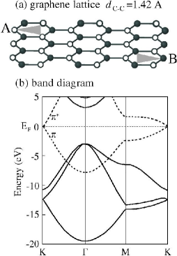
Graphene is a single atomic layer of graphite [see the graphene lattice in Fig. 1(a)] produced for the first time by mechanical exfoliation of graphite nov2004 . The carbon atoms in graphene are arranged in a hexagonal lattice and are covalently bonded via hybridization. Three of the four valence electrons in each carbon atom make three bonds with its nearest neighbors. The covalent bond provides strong binding between the carbon atoms but the electrons contribute poorly to the conductivity. One half-filled orbital left on each carbon atom, after its covalent bonding with the neighbors, is orthogonal to the graphene plane. The interaction of the orbitals residing on the nearest-neighboring carbon atoms results in the generation of the bonds below and above the graphene plane. The electrons are delocalized across the entire lattice and contribute to the conductivity of graphene. In the band diagram the - electrons are distinguished by the and bands formed at the top of the valence band and at the bottom of the conduction band, respectively, as shown in Fig. 1(b) amara . These bands meet and become cone shaped at the K-points such that they are degenerate and display a linear dispersion near the K-points resulting in zero effective mass for electrons and holes and high mobility of the charge carriers julia1 .
Graphene exhibits many attractive material properties that are important for building electronic devices. These include high mobilities of charge carriers, high current-carrying capabilities, high transparency, high thermal conductivity and mechanical stability. But, despite all these impressive qualities, the absence of a bandgap in graphene, which renders it a semi-metal, is a major obstacle in developing graphene based electronic devices. As in all semiconductor systems, the presence of a bandgap is essential for electronic control of the conductivity. The zero effective mass of electrons and holes in graphene creates yet another problem. The charge carriers in graphene can not be confined by the potential barriers which is, in fact, transparent for these massless particles (due to Klein tunneling).
The lack of a bandgap in graphene has attracted considerable attention from the researchers in search of a mechanism for opening a gap between the and bands. In fact, the shape and size of the graphene flakes play a crucial role in defining its electronic properties nakada . Small flakes have been found to possess a gap which is found to be suppressed and exhibit an oscillatory behavior with increasing width of the structures along the zigzag edges. A reduction of the gap with increasing size of the graphene flakes has indeed been confirmed experimentally han2007 ; ritter2009 . Occurrence of the gap was proposed to be induced by the quantum confinement effect in the flakes of small size. However, it was also shown that the specific ordering of the localized states at the zigzag edges of graphene (when localized states are ferromagnetically ordered along the zigzag edge and antiferromagnetically between the opposite zigzag edges) would break the sublattice symmetry of graphene and, therefore, can also open a gap pisani ; son2006 . The oscillatory behavior has been attributed to the shape of the edges nakada .
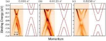
The idea of opening of an energy gap by breaking one of the symmetries in graphene (sublattice or lattice) has received wide recognition in the scientific community ohta-sci313 ; wehling2008 ; julia_ads . It was found that any alteration of the ideal hexagonal lattice of graphene by defects would break the lattice symmetry of graphene, while the unequal charge exchange of different graphene sublattices with the substrate or adsorbates breaks the sublattice symmetry, thereby generating a gap. Experimentally, it was shown that graphene on a substrate indeed possesses a gap ohta-sci313 . It was also found that the charge exchange with the substrate or with the adsorbates would dope graphene and the type of doping (- or -type) can be controlled by the type of molecule that is adsorbed, i.e. the acceptor or the donor ohta-sci313 ; wehling2008 . The experimental data on alteration of the band structure of the bilayer graphene on SiC substrate with adsorption of potassium is displayed in Fig. 2. In as-prepared samples of graphene, the charge accumulated on the surface of graphene and the depleted SiC substrate create a built-in dipole field which leads to the opening of a gap through breaking of the graphene symmetry [see Fig. 2 (a)]. Potassium adsorbed on the graphene surface dopes graphene and alters that dipole field, thereby modifying the size of the bandgap. When the number of transferred electrons per unit cell is 0.0125 ē the built-in dipole field is neutralized and the gap is closed (see Fig. 2 (b)), while a further increase in concentration of the transferred electrons leads to reopening of the gap [see Fig. 2 (c)]. Because potassium is a donor of electrons the charge exchange between potassium and graphene shifts the bands of graphene down according to the position of the Fermi level.
II Graphane – hydrogenated graphene
The strong influence of molecular adsorption on the electronic properties of graphene has made this topic very popular among the researchers bouk ; julia_ads . Most adsorbed molecules interact weakly with pure graphene holding on to its surface or at the edges via the van der Waals forces. However, some adsorbates can bind to the carbon atoms in graphene which not only breaks the lattice symmetry but also modifies the hybridization of the carbon bonds bouk . For example, bonding of a carbon atom with adsorbate possessing one valence electron, such as H or Li sofo ; yang ; bouk , leads to moving of this carbon atom out of the graphene plane and change the carbon bonds connecting this atom with its neighbors from the hybridization to . In the case when all the carbon atoms are hydrogenated, the planarity of the graphene lattice is destroyed giving rise to a new lattice type which can adopt two main conformations: the so-called ‘boat’ and ‘chair’ conformations sofo . In the boat conformation, hydrogenation of the carbon atoms occurs in pairs, i.e., pairs of nearest-neighbor carbon atoms are hydrogenated on the same side of the plane. However, the repulsion between two paired hydrogen atoms leads to instability of this conformation. The chair conformation is more stable because the nearest-neighbor carbon atoms, which belong to different sublattices, are hydrogenated from different sides of the graphene plane. The structure of the chair conformation is shown in Fig. 3 (a). For this conformation, hydrogenation causes one sublattice to move out of the crystal plane, mimicking other -bonded crystal, such as diamond. Therefore, the carbon atoms in ideal graphane (fully hydrogenated on both sides of a graphene lattice) lattice form two separate planes and for each plane the trigonal symmetry of the carbon atoms belonging to A- or B-sublattices is preserved.
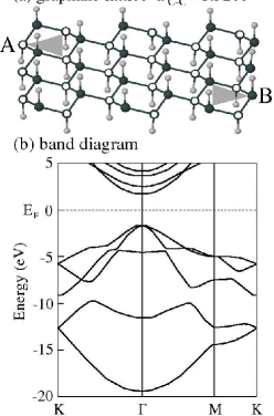
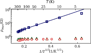
The electronic structure of graphane was reported for the first time in theoretical work sofo . The band diagram obtained there is presented in Fig. 3 (b). All four valence electrons belonging to the carbon atoms participate in the formation of the covalent bonds and therefore the bands are removed from the band structure of graphane. As a result of the absence of the bands, which in graphene was responsible for the gapless nature of its electronic structure, graphane is a semiconductor characterized by a wide direct gap at the point sofo . Moreover, transformation of the carbon bonds from the to hybridization results in an increase in the bond length from 1.42 Å [see Fig. 1 (a)] to 1.52 Å [see Fig. 3(a)]. Subsequently, it was experimentally confirmed that hydrogenation of graphene alters its lattice structure resulting in the hybridization of the carbon bonds ryu2008 that indeed alters the behavior of graphene in an electric field from conducting to insulating elias2009 . The resistivity of pristine graphene and hydrogenated graphene as a function of temperature are plotted in Fig. 4. Hydrogenation of graphene has been found to be reversible ryu2008 ; elias2009 , which is a definite advantage for application of graphene/graphane in nanoscale electronics. Moreover, the combination of pure and hydrogenated graphene distinguished by the different size of the bandgap is promising for creation of periodic multi-quantum arrays that facilitates the resonant charge transfer chernoz2007 .
III Magnetc properties of graphane
In the original theoretical work where graphane was proposed sofo , hydrogenation was performed from both sides of the graphene plane while in available experiments ryu2008 ; elias2009 graphene on a substrate was hydrogenated only from one side. Quite naturally, later theoretical work zhou has focused on the electronic properties of free-standing graphene, hydrogenated from one side (which was christened graphone). It was claimed that graphone is a ferromagnetic semiconductor with a small indirect gap (=0.46 eV) zhou . Ferromagnetism in graphone is attributed to the presence of localized states on the non-hydrated side.
In graphane each H-vacancy defect, which leaves an unsaturated dangling bond released on the carbon atom generates a localized state characterized by the unpaired spin. This spin-polarized state creates a defect level in the bandgap of graphane julia . The band diagram of a finite size graphane (the size of the bandgap of defect-free graphane was =7.51 eV in Ref. julia ) containing a single H-vacancy defect is shown in Fig. 5 (a). In the case of a single defect in graphane, the bandgap – the energy difference between the lowest unoccupied (LUMO) and the highest occupied molecular orbitals (HOMO) – is suppressed due to the appearance of the defect level between the HOMO and LUMO of the defect-free graphane. For the -spin state, the H-vacancy induces a defect level closer to the valence band which becomes the new HOMO, while for the -spin state – closer to the conduction band generating a new LUMO. As a result, the HOMO-LUMO gaps for the - and -spin states are significantly shifted in energy.
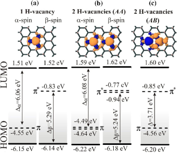
If there are two or more H-vacancies in graphane, the spins of the localized states can be ferromagnetically or anti-ferromagnetically ordered (see Fig. 5 (b,c)). The ordering is defined by the distribution of the defects between the sides of the graphene plane, i.e., their actual presence in different sublattices. Therefore, if the two H-vacancy defects are located on the same side of the graphane plane (AA distribution) then the two localized states reside on the same sublattice. In graphene we already know that for two states on the same sublattice if their spins are antiparallel then the destructive interference between the spin-up and spin-down tails of these states leads to an enhancement of the total energy of the system son . Therefore, in both graphene and graphane, if the two states are localized on the same sublattice (AA distribution), the ferromagnetic ordering of their spins is energetically preferable. For the states localized on different sublattices (AB distribution), achieved in graphane by removing the hydrogen atoms from different sides of the graphane plane, antiferromagnetic ordering of the spins lowers the total energy of the system. Ferromagnetic and antiferromagnetic ordering of the spins versus the sublattice symmetry are in line with Lieb’s theorem lieb .
The destructive and constructive interference between the spin-up and spin-down tails of the localized states decrease exponentially with increasing distance between the states son . For the AA distribution, ferromagnetic ordering of the spins is energetically preferable for , otherwise, the interference of the tails is negligible and the difference of the total energies between the states characterized by different spin ordering is less than eV julia . Therefore, one can conclude julia that the ferromagnetic ordering of spins of the localized states in graphane is possible only for the H-vacancy defects located on the neighboring carbon atoms.
Ferromagnetic ordering of spins makes graphane containing the vacancy defects a ferromagnetic wide gap semiconductor. Because each vacancy can generate a magnetic moment of , where is the Bohr magneton, the magnitude of magnetism can be manipulated by the vacancy concentration (). However, increasing vacancy concentration can make it difficult to maintain the ordering of the spins even when the vacancies are placed close to each other. Thus it was found that with an increasing number of H-vacancy defects, the state characterized by the highest magnetic moment gets closer in energy to several states of lower magnetic moment (when is less than the number of vacancies), thereby limiting the magnitude of maximum magnetization. Moreover, there is a critical number of defects 8 when the energy difference between the state of ferromagnetic and antiferromagnetic ordering rapidly decreases (for =8, =6.56 eV while for =10, =0.25 eV), thereby destabilizing the ferromagnetic state. The lattice relaxation of graphane induced by the presence of defects also destabilizes the ferromagnetic state. Moreover, we believe that the non-uniform distribution of the hydrogen atoms over the graphane plane found in flores (showing that the sequence of the up and down H atoms would be broken) would also have some issues in maintaining ferromagnetic ordering of the spins.
IV Application in nanoscale electronics
The unique electronic properties of both graphene and graphane makes them excellent candidates for nanoscale electronics. The influence of the substrate and the type of molecules adsorbed on the graphene surface on the electronic properties can be used to tune the size of the bandgap and the doping in the production of nanoscale devices. It has, for example, already been applied in developing gas sensors with sensitivity at the level of a single molecule wehling2008 . In graphane, the size of the gap can be manipulated by inducing the H-vacancy defects julia or through the interaction of these vacancies with adsorbates.
The magnetic properties of graphene and graphane are also fascinating. Dependence of the ordering of spins of electrons in the localized states on their distribution between the sublattices is unique and suitable for application of graphene/graphane in spintronics and magnetoelectronics. Therefore, for graphene whose zigzag edges possess the localized states such that the spin-up and spin-down states are spatially separated between the opposite edges, half-metallicity of can be obtained by the application of an external electric field son2006 , by chemical functionalization or substitutional doping at the zigzag edges julia2 . Moreover, the imbalance in the distribution of the localized states between the sublattices (for example, by distribution of the defects predominantly on one sublattice) creates the non-zero magnetization in graphene/graphane.
The unique electronic and magnetic properties of graphene/graphane are expected to contribute significantly in future applications in nanoscale electronics. However, to make that a reality we must be able to control of shape and quality of the edges of graphene/graphane structures. In most of the methods developed for fabrication of graphene, such as exfoliation of graphite nov2004 , lithographic patterning lit and chemical sonication sonic , the control of the flake size and quality of the edges are really poor. However, recently developed methods involving the unzipping of carbon nanotubes nature1 ; nature2 are very promising. It has been claimed that unzipping by plasma etching provides smooth edges and a small range of nanoribbon width (10-20 nm) nature1 . The second unzipping method – the solution-based oxidative process – allows one to perform the longitudinal cut of the nanotubes thereby creating flakes with predominantly straight linear edges nature2 . In graphane, for which the fluctuation of the shape and sizes of the flakes would not crucially influence its electronic properties because of the large bandgap, the main problem to be solved is a controllable dehydrogenation. The application of graphene and graphane in nanoscale electronics will have to wait until those technological issues are resolved satisfactorily.
V Acknowledgements
This work has been supported by the Canada Research Chair program and the NSERC Discovery Grant.
References
- (1) Electronic mail: tapash@physics.umanitoba.ca
- (2) D.S.L. Abergel, V. Apalkov, J. Berashevich, K. Ziegler and T. Chakraborty, Adv. Phys. (in press).
- (3) T. Chakraborty, Physics in Canada 62, 351 (2006).
- (4) K.S. Novoselov, A.K. Geim, S.V. Morozov, D. Jiang, Y. Zhang, S.V. Dubonos, I.V. Grigorieva and A.A. Firosov, Science 306, 666 (2004).
- (5) H. Amara, S. Latil, V. Meunier, Ph. Lambin, J.-C. Charlier, Phys. Rev. B. 76, 115423 (2007).
- (6) K. Nakada, M. Fujita, G. Dresselhaus and M. S. Dresselhaus, Phys. Rev. B 54, 17954 (1996).
- (7) M.Y. Han, B. Özyilmaz, Y. Zhang and P. Kim, Phys. Rev. Lett. 98, 206805 (2007).
- (8) K.A. Ritter and J.W. Lyding, Nature Mat. 8, 235 (2009).
- (9) L. Pisani, J.A. Chan, B. Montanari and N.M. Harrison, Phys. Rev. B 75, 064418 (2007).
- (10) Y.-W. Son, M.L. Cohen and S.G. Louie, Nature 444, 347 (2006).
- (11) T. Ohta, A. Bostwick, T. Seyller, K. Horn, and E. Rotenberg, Science 313, 951 (2006).
- (12) T.O. Wehling, K.S. Novoselov, S.V. Morozov, E.E. Vdovin, M.I. Katsnelson, A.K. Geim and A.I. Lichtenstein, Nano Lett. 8, 173 (2008).
- (13) J. Berashevich and T. Chakraborty, Phys. Rev. B 80, 033404 (2009).
- (14) J.O. Sofo, A.S. Chaudhari and G.D. Barber, Phys. Rev. B 75, 153401 (2007).
- (15) C.-K. Yang, Appl. Phys. Lett. 94, 163115 (2009).
- (16) D.W. Boukhvalov and M.I. Katsnelson, Phys. Rev. B 78, 085413 (2008).
- (17) S. Ryu, M.Y. Han, J. Maultzsch, T.F. Heinz, P. Kim, M.L. Steigerwald and L. E. Brus, Nano Lett. 8, 4597 (2008).
- (18) D.C. Elias, R.R. Nair, T.M.G. Mohiuddin, S.V. Morozov, P. Blake, M.P. Halsall, A.C. Ferrari, D.W. Boukhvalov, M.I. Katsnelson, A.K. Geim and K.S. Novoselov, Science 323, 610 (2009).
- (19) L.A. Chernozatonski, P.B. Sorokin and J.W. Brüning, Appl. Phys. Lett. 91 (2007), p. 183103.
- (20) J. Zhou, Q. Wang, Q. Sun, X.S. Chen, Y. Kawazoe and P. Jena, Nano Lett. 9 (2009), p. 3867.
- (21) H. Lee, Y.-W. Son, N. Park, S. Han and J. Yu, Phys. Rev. B 72, p. 174431 (2005).
- (22) E.H. Lieb, Phys. Rev. Lett 62 (1989), p. 1201.
- (23) J. Berashevich and T. Chakraborty, Phys. Rev. .. (), p. .
- (24) M.Z.S. Flores, P.A.S. Autreto, S.B. Legoas and D.S. Galvao, Nanotechnology 20 (2009), p. 465704.
- (25) J. Berashevich and T. Chakraborty, Phys. Rev. B 80 (2009), p. 115430.
- (26) Z.H. Chen, Y.M. Lin, M.J. Rooks and P. Avouris, Physica E 40, 228 (2007); M.Y. Han, B. Ozyilmaz, Y.B. Zhang and P. Kim, Phys. Rev. Lett. 98, 206805 (2007).
- (27) X.L. Li, X. Wang, L. Zhang, S. Lee and H. Dai, Science 319, 1229 (2008).
- (28) L. Jiao, L. Zhang, X. Wang, G. Diankov and H. Dai, Nature 458, 877 (2009).
- (29) D.V. Kosynkin, A. Higginbotham, A. Sinitskii, J.R. Lomeda, A. Dimiev, B.K. Price and J. Tour, Nature 458, 872 (2009).