Local Measurement of Microwave Response with Local Tunneling Spectra Using Near Field Microwave Microscopy
Abstract
We have fabricated near-field scanning microwave microscope and measured the local microwave response and the local density-of-states (LDOS) in the area including the boundary between the Au deposited and the non-deposited region on highly-orientated pyrolytic graphite at a frequency of about 7.3 GHz. We have succeeded in measuring both the LDOS and the surface resistance. It can be observed that the surface resistance in Au deposited region with the metallic tunneling spectra is smaller than that in the non-deposited region with the U-shaped tunneling spectra.
Scanning tunneling microscope (STM) has been used in the scanning tunneling spectroscopy (STS) mode to investigate a variety of issues such as probing the local density-of-states (LDOS) within the superconducting vortex cores [1, 2], elucidating the inhomogeneous distribution of superconducting gap in high temperature superconductors [3], studying the edge states in graphite sheet [4], capturing the LDOS in carbon nano-tubes [5], and so on. On the other hand, near-field scanning microwave microscope (NSMM) enables us to measure locally the microwave response (MWR) from a sample. For example, the local dielectric coefficient in (Ba, Sr)TiO3 [6] and the local surface resistance () in YBa2Cu3O7-δ [7] have been visualized by the NSMM at mm or m length scale. Recently, an STM-assisted NSMM has been designed [8] to integrate the functionality of both the STM and the NSMM.
Imtiaz et al. achieved the spatial resolution of less than 100 nm by using the STM-assisted NSMM [8, 9]. They claimed that the spatial resolution of the MWR approaches the value of the radius of curvature at the end of the STM tip (), when the distance between the tip and the sample is much less than . Until now, the local measurements have been done for the materials with relatively high of more than the order of 10 /sq. by a sharp tip with of less than a few m [8, 10, 9]. When the is lower than a few /sq., the rate of change in the MWR with respect to the change in becomes very small using the sharp tip [8, 10, 9]. For this reason, it was difficult to measure the local variation in in low materials. Even though an STM-assisted NSMM holds the capability to measure both the local and the LDOS, the spatial variation of these quantities has not been compared yet.
The measurement of LDOS and local can reveal how the local variation of DOS due to impurities, defects, grains, carrier segregations, and so on, affects the local resistance on nano-meter length scales. It is quite important to understand the electronic states around the local disorders. In this study, we have succeeded in obtaining the clear difference in the MWR and LDOS near the boundary. We show the measurements of LDOS and local in low materials. As a suitable sample, we use the boundary between Au deposited and non-deposited region on highly-orientated pyrolytic graphite (HOPG) whose is the order of 0.1 /sq, because of the following three reasons: (i) the surfaces of HOPG and Au are stable so as to obtain good tunneling spectra, (ii) there is a clear difference between the surface structures, and, (iii) these have low surface resistances.
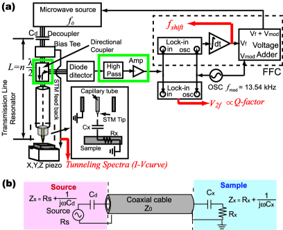
The NSMM design used in the experiments is based on that in ref. 8. The transmission line resonator in the NSMM consists of the bias tee (IMMET 8810E), the directional coupler (HP87301D), and the coaxial cable whose impedance is 50 , as shown in Fig. 1(a). One end of the resonator is connected to the home-made decoupling capacitor (labeled ”Decoupler” in Fig. 1(a), = 0.15 pF). The other end terminates at an open-ended coaxial probe. This open-ended coaxial probe is just a piece of coaxial cable, in which a stainless steel capillary tube, holding the STM tip, replaces the center conductor. The bias tee permits us to use the same tip for both STM and microwave microscope. The reflected wave travels via the directional coupler to the diode detector (HP 8473C). This detector produces a voltage signal, which is proportional to the power of the reflected wave from the resonator. The output from this detector is sent to the two lock-in amplifiers referred at the external oscillator frequency (= 13.54kHz). The frequency-feedback-circuit (FFC) including one lock-in amplifier as marked out by dashed box in Fig. 1(a) keeps microwave source locked to a resonant frequency of the resonator. The voltage output from the FFC is proportional to the shifts in the resonant frequency (f). In this case, this frequency rate is 10 MHz/V. This output voltage is added to the voltage oscillating at the frequency of the oscillator. The added voltage is used to modulate the source frequency at . The deviation of the frequency modulation is corresponding to the amplitude of the oscillated voltage from the oscillator and is set to be 5 MHz in the measurement. The detailed information with respect to the FFC can be seen in ref. 8. The lock-in amplifier outside the dashed box in Fig. 1(a) picks up the signal at 2 [labeled as in Fig. 1(a)], which gives a measure of the quality factor (Q) of the resonator. In the apparatus, following two differences from the design in ref. 8 have been adopted to pick up a minute change of the signal [as shown by the green boxes in Fig. 1(a)]: (i) we put the directional coupler into the resonator to enhance the measured power of reflective wave from the sample, and (ii) we append the high-pass filter and the preamplifier to the system, to improve the signal noise ratio. The STM used was manufactured by UNISOKU. The STM feedback system can keep the tip-sample distance a few nm. This system allows us to measure simultaneously the four independent signals; the frequency shift (f), the quality factor (Q), the STM topography, and the local tunneling spectrum.
The resonator can be modeled as a resonant coaxial transmission line of the total length (=1.7114 m) with a capacitor and a resistance as shown in Fig. 1(b). In this model, resonant frequency f and Q are expressed by eqs. (1) and (2), respectively [11].
| (1) |
| (2) |
where is the impedance of coaxial cable (= 50 ), and . Both quantities are dependent on the , corresponding to the tip-sample separation, and the sheet resistance of the sample . and are constants related to the impedance mismatching at the position of the decoupling capacitor, as expressed below.
| (3) |
| (4) |
where is the mode number (= 118), is the transmission line attenuation constant (0.49 Np/m), and is the internal impedance of the source (= 50 ). The local and values can be estimated from the locally measured resonant frequency and the quality factor at each location by using following two equations.
| (5) |
| (6) |
where and are the normalized resonant frequency and quality factor by the resonant frequency (= 7.30445 GHz) and the quality factor without sample, respectively: and ( = 5.349 V).
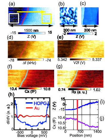
To confirm the validity of the measurement of the LDOS and the local , we used the boundary between the Au deposited and non-deposited region in the partially Au deposited HOPG, where the thickness of the deposited Au was 40 nm. The measurements were performed in air at room temperature. The probe tip used is mechanically etched Pt-Ir tip whose is about a few hundred nm. Figure 2(a) shows an STM image in the area including the boundary (red line) between the Au deposited (right side) and non-deposited region on HOPG (left side). On the left side from the boundary, the topography is almost flat. As the tip moves towards the right side from the boundary, the altitude gradually increases, as shown in Fig. 2(i). Figures 2(b) and 2(c) are the fine images of the regions surrounded by the yellow and white squares in Fig. 2(a), respectively. In Fig. 2(b), there are granular structures as expected on the Au surface [8]. On the other hand, in Fig. 2(c), the step structures and the flat terraces as expected on the HOPG [4] can be observed. Figures 2(d) and 2(e) show the and maps in the same field of view of Fig. 2(a). In spite of the low in the sample, these maps display the clear contrasts which are similar to the topography. As shown in Figs. 2(f) and 2(g), the local and were calculated from and maps by using eqs. (5) and (6). In these maps, one can see the inverse contrast against the topography. The start to decrease as going to the right side from the boundary, as shown in Fig. 2(j). When the STM is in the constant-current-mode, the probe follows the topography of the sample as the distance between the tip and the sample is kept to be constant. As the tip goes from the left to the right side, the capacitance becomes small as shown in Fig. 3(a), which is the first order approximation based on the models in refs. 8 and 9. As a result, it can be expected that the spatial variation of shows the reverse change from the surface topography, during the scanning operation. Thus, the contrast in the map reflects the surface topography.
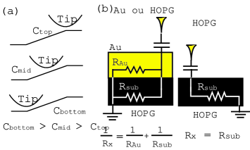
The values in the map have been scaled by the averaged value in the HOPG region, because it is difficult to estimate the absolute value of due to the strong dependence of the on the tip geometry [8, 9]. The in the Au region is smaller than that in HOPG region, as shown in Fig. 2(g). The measured surface resistances in Au deposited region should be considered as the combined resistance of the (= , is the thickness of Au) and (=, is the skin depth of HOPG whose value is about 4 m) which is added in parallel with , as shown in Fig. 3(b): 1/ =1/ + 1/ . On the other hand, in non-deposited region, the should contain only : = . Based on this perspective, the in Au deposited region is about 20% small against the in non-deposited region, which is the nearly same as that in the observation.
In addition to the spatial variation of , the clear differences in tunneling spectra between Au deposited region and non-deposited region, which are proportional to the LDOS, can be observed, as shown in Fig. 2(h). The LDOS in Au deposited region hardly depends on the energy as expected for the LDOS in Au. On the other hand, U-shaped tunneling spectrum has been obtained in non-deposited region. This U-shaped spectrum has been also observed in the STS experiments using normal STM [4].
The results in this study indicate the capability of the system to measure the local and the LDOS at nano-scale. Consequently, the STM-assisted NSMM can provide the relation between LDOS and the local around an object which disturbs the local electronic properties. Additionally, it is conceivable that the apparatus is suitable for the local measurement of the electron spin resonance in magnetic materials, the penetration depth measurements in superconductors, and the resistance in nano-particles and nano-wires.
In summary, we have demonstrated the local measurement of the tunneling spectra and the sheet resistance in the area including the boundary between the Au deposited and non-deposited region on HOPG by using the NSMM. Both the clear contrast in the local sheet resistance and the difference of tunneling spectra has been observed around the boundary simultaneously. Our STM-assisted NSMM can measure the local density-of-states and local surface resistance in nano-scale. This system is useful tool to study the effect of a local disorder on the electrodynamics and to measure the local properties in nano-materials.
References
- [1] H. F. Hess, R. B. Robinson, R. C. Dynes, J. M. Valles, Jr., and J. V. Waszczak: Phys. Rev. Lett. 62 (1989) 214.
- [2] K. Matsuba, S. Yoshizawa, Y. Mochizuki, T. Mochiku, K. Hirata, and N. Nishida: J. Phys. Soc. Jpn. 76 (2007) 063704
- [3] T. Machida, Y. Kamijo, K. Harada, T. Noguchi, R. Saito, T. Kato, and H. Sakata: J. Phys. Soc. Jpn 75 (2006) 083708.
- [4] Y. Niimi, T. Matsui, H. Kambara, K. Tagami, M. Tsukada, and H. Fukuyama: Phys. Rev. B. 73 (2006) 085421.
- [5] A. Hassanien, Y. Kumazawa, H. Kataura, Y. Maniwa, S. Suzuki, Y. Achiba, and M. Tokumoto: App. Phys. Lett. 73 (1998) 3839.
- [6] D. E. Steinhaurer, C. P. Vlahacos, C. Canedy, A. Stanishevsky, J. Melnganilis, R. Ramesh, F. C. Wellstood, and S. M. Anlage: App. Phys. Lett. 75 (1999) 3180.
- [7] D. E. Steinhaurer, C. P. Vlahacos, S. K. Dutta, B. J. Feenstra, F. C. Wellstood, and S. M. Anlage: App. Phys. Lett. 72 (1998) 861.
- [8] A. Imtiaz and S. M. Anlage: J. App. Phys. 100 (2006) 044304.
- [9] A. Imtiaz and S. M. Anlage: Ultramicroscopy 94 (2003) 209.
- [10] A. Imtiaz and S. M. Anlage: App. Phys. Lett. 90 (2007) 143106.
- [11] Steven M. Anlage, Vladimir V. Talanov, and Andrew R. Schwartz: ”Principles of Near-Field Microwave Microscopy,” in Scanning Probe Microscopy: Electrical and Electromechanical Phenomena at the Nanoscale, ed. S. V. Kalinin and A. Gruverman (Springer-Verlag, New York, 2006), p. 207-245