Cryogenic scanning force microscopy of quantum Hall samples:
Adiabatic transport originating in anisotropic depletion at contact interfaces
Abstract
Anisotropic magneto resistances and intrinsic adiabatic transport features are generated on quantum Hall samples based on an (Al,Ga)As/GaAs heterostructure with alloyed Au/Ge/Ni contacts. We succeed to probe the microscopic origin of these transport features with a cryogenic scanning force microscope (SFM) by measuring the local potential distribution within the two-dimensional electron system (2DES). These local measurements reveal the presence of an incompressible strip in front of contacts with insulating properties depending on the orientation of the contact/2DES interface line relatively to the crystal axes of the heterostructure. Such an observation gives another microscopic meaning to the term ’non-ideal contact’ used in context with the Landauer-Büttiker formalism applied to the quantum Hall effect.
pacs:
73.43.-fFor now more than one decade, cryogenic scanning force microscopy (SFM) has been used to probe the electrostatic potential distribution in two-dimensional electron systems (2DES) realized in (Al,Ga)As/GaAs heterostructures under quantum Hall conditions mccornick4654 ; weitz247 ; *ahlswede562; *ahlswede165. Those measurements have demonstrated the important role of compressible and incompressible strips chklovskii+shklovskii+glazman4026 ; *lier+gerhardts7757; *siddiki+gerhardts125315; *siddiki+gerhardts195335 for the current distribution in quantum Hall samples. Despite of these experimental findings, the edge state picture buttiker9375 remains the widely used model to describe the magneto-transport in quantum Hall devices, also in the context of topological insulators roth294 ; *buttiker278. Its success has been partly legitimated by its ability to include contact effects 111In controlled experiments, ’ideal and non-ideal’ contact properties are mimiced by locally depleting the 2DES by gate electrodes in front of contacts. and to explain adiabatic magneto transport features haug131 ; *vonHouten+Beenaker1 – like the disappearance of peaks in the Shubnikov-de Haas oscillations, the extension of quantum Hall plateaus to lower magnetic fields and the existence of non-local resistances komiyama+nii7 ; *alphenaar677; *mceuen2062; *wees8066. In this letter we manage a comparison between magneto transport and scanning force microscopy investigations on Hall bar samples showing adiabatic transport features without the use of gates. The SFM measurements clearly present potential distributions from which we conclude that the incompressible strip in front of alloyed contacts possesses different insulating properties depending of the orientation relatively to the crystal axes of the underlying heterostructure. This result shows how to interpret adiabatic features in terms of compressible/incompressible strips and what is the microscopic origin of anisotropy in magneto resistances.
 |
The samples used here are based on an (Al,Ga)As/GaAs heterostructure containing the 2DES at the heterojunction interface 60 nm below the surface. The electron density and mobility are respectively and at K. These conditions lead to for the electron mean free path, which is three time larger than those of the samples measured in weitz247 ; *ahlswede562; *ahlswede165. High electron mobility Hall bars as depicted in Fig. 1 are defined by optical lithography and wet etching. Following our standard recipe goktas1579 , Au/Ge/Ni film is alloyed to achieve low resistive contacts to the 2DES. After annealing, the remaining 2DES has a size of about 10 width and 58 length, which is comparable to the scanning range 20 by 20 of our cryogenic SFM. From transmission line measurements goktas1579 , we also find on these samples an anisotropy in contacting the 2DES in [01-1] or in [011] crystal direction which is a general property of alloyed Au/Ge/Ni contacts kamada1263 ; goktas1579 . Here the specific resistivity (w, the width of the borderline between 2DES and alloyed metal) is for contacts with their borderline perpendicular to [011], and for contacts with their borderline perpendicular to [01-1].
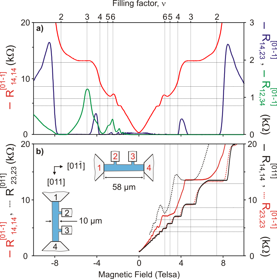
To obtain the magneto resistance (Hall bar oriented along [01-1]), an ac current of 100 nA rms amplitude is biased via contacts and , and the ac voltage drop between contact and is measured by lock-in technique. In comparison to a standard six-terminal Hall bar of same size, the four-terminal Hall bars with two contacts on one side of the mesa display in some magneto resistances generic adiabatic transport features, reproduced on many samples of same geometry. Examples are given in Fig. 1a: (1) In measuring the four-terminal longitudinal resistance , resistance peaks of the Shubnikov-de Haas (SdH) oscillations are completely suppressed in between and , and in between and 222The filling factor is obtained from the electron density and magnetic field by .. (2) The non-local resistance asymmetrically changes with the magnetic field orientation, i.e. for positive magnetic field no voltage drop is observed between contact 3 and 4 (), while for negative sign non-zero resistance values are measured. (3) For the two-terminal resistance , Hall plateaus with are shifted to lower magnetic field values corresponding to filling factors around . In general we found that if one of two contacts has its interface line with the 2DES perpendicular to [01-1], Hall plateaus in the two-terminal measurements (, ) are shifted to lower magnetic field values. The effect becomes most striking when directly comparing and of two Hall bars of same geometry but either oriented along [011] or [01-1] crystal direction (see Fig. 1b): The two-terminal Hall resistances and superpose whereas and deviate. All these deviations (1) to (3) in the magneto resistances have been described in literature and are usually interpreted within the edge-state picture as a non-equilibrium situation between edge states running along the same edge, caused by full or partial reflection of edge states at imperfect contacts haug131 . The contacts here are however state-of-the-art for both orientations, i.e. good ohmic and low resistive. Furthermore, we succeed to generate intrinsic adiabatic transport features by simply selecting the mesa orientation and its geometry oswald235331 .
 |
To find the microscopic origins of the previously described adiabatic transport features, the measurements of the Hall potential distribution within the 2DES have been performed by using a scanning force microscope operating at 1.3 K up to 13 Tesla weitz349 . After finding the Hall bar structure at low temperature in an usual SFM contact mode, the tip is retracted and made oscillating 70 nm above the mesa surface to probe only electrostatic forces. A constant bias voltage is applied between 2DES and metalized cantilever tip compensating for work function differences and avoiding a gating effect on the 2DES by the tip. As the 2DES is buried in the heterostructure, a special calibration technique weitz349 has to be used for extracting the Hall potential, i.e. the change of the local electrostatic voltage with current flow through the sample. In a first scan, a 15 mV excitation at 3.4 Hz is applied to the whole 2DES and the modulation amplitude of the cantilever resonance frequency shift is recorded by lock-in technique along the mesa width. This signal – being proportional to the local excitation, is almost constant with some local variations due to the donor and surface charges embedded between 2DES and cantilever tip: . A second scan is run at the same line with the potential excitation applied only to one contact whereas a second contact is grounded. A 3.4 Hz ac current flows through the sample and the related Hall potential distribution can be detected by a new measurement: . The ratio between second and first scan delivers the normalized Hall potential profile with a spatial lateral resolution better than 100 nm weitz349 .
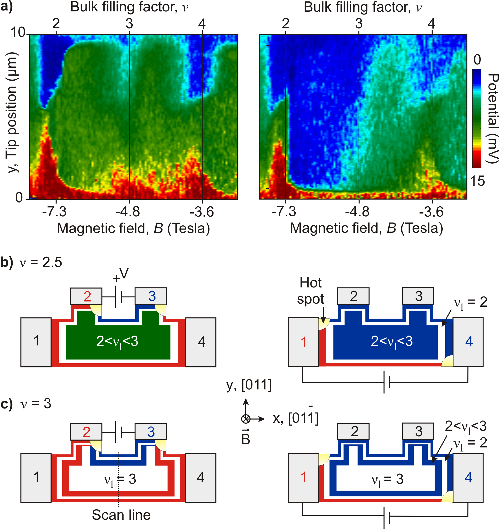
In Fig. 2a, the scanned potential profiles under the condition for measuring and are presented in a colorscale for negative magnetic field (i.e. clockwise rotation of electrons on cyclotron orbits) ranging from below to above . The scans are taken in the middle of the 10 wide mesa as indicated in the Hall bar sketches (Fig. 2b,c). The colors blue, green and red in the plots correspond to the lowest, middle and highest potential value, respectively. The profiles displayed in Fig. 2a(left) reflect the results also obtained in the past on samples with lower electron mobility of 50 ahlswede562 : The Hall potential drops on both sides of the Hall bar almost symmetrically at the expected positions of the innermost incompressible strips which merge around covering the whole bulk of the 2DES. At this latter filling factor the Hall potential drop is then widely spread in the bulk and , shown in Fig. 1b, behaves normal.
The situation is different in Fig. 2a(right), where the change of potential happens completely on the lower side of the mesa [AsimilarprofilewasobservedonagatedHallbarby]woodside238. This behaviour is visible for the whole range between and , and is still strongly pronounced above . In this regime the bulk of the 2DES being compressible with , the complete Hall potential drop happens between the compressible bulk and the compressible edge over the incompressible strip at the lower mesa side [see Fig. 2b(right)]. The current is thus driven without dissipation within this strip by the complete Hall voltage , 333The current is hence concentrated in a region of carrier density smaller than the bulk density as it was expected from the shift of Hall plateaus to lower magnetic fields.. As the longitudinal resistance vanishes at these filling factors and for both magnetic field signs, we can state that there is no equilibration between the compressible bulk with and contacts 1 and 4 [see Fig. 2b(right)]. This decoupling comes from the depletion region in front of contacts 1 and 4 which have an enough smooth gradient towards the bulk to create a wide incompressible strip, which isolates the compressible edge and bulk under high voltage drops (For reminder, contacts with such orientation have a higher specific contact resistivity at zero magnetic field). Turning around the mesa orientation and measuring , the usual transport is obtained (see Fig. 1b), i.e. the isolating property of the incompressible strip in front of contacts 1 and 4 with its interface line perpendicular to [011] is not pronounced at (Such contacts have a lower specific contact resistivity at zero magnetic field). To indicate the different isolating properties of incompressible strips in front of the contacts, their widths are marked smaller or wider in Fig. 2b,c. At lower magnetic field, the two-terminal resistance shows a Hall plateau with (see Fig. 1a) even at where the bulk is mainly incompressible [see Fig. 2c(right)]. It follows that the compressible strip with which encircles the incompressible bulk, stays isolated from the compressible edge with by the incompressible strip . The potential drop is hence located between the two compressible strips at the lower mesa side, – a situation which reminds on the adiabatic transport model of non-equilibrium between edge states.
 |
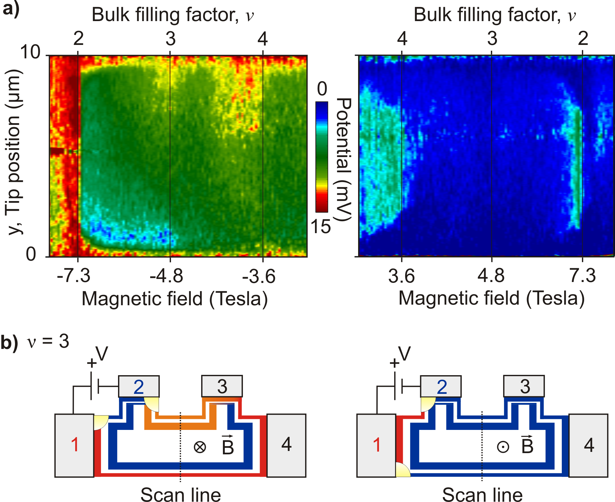
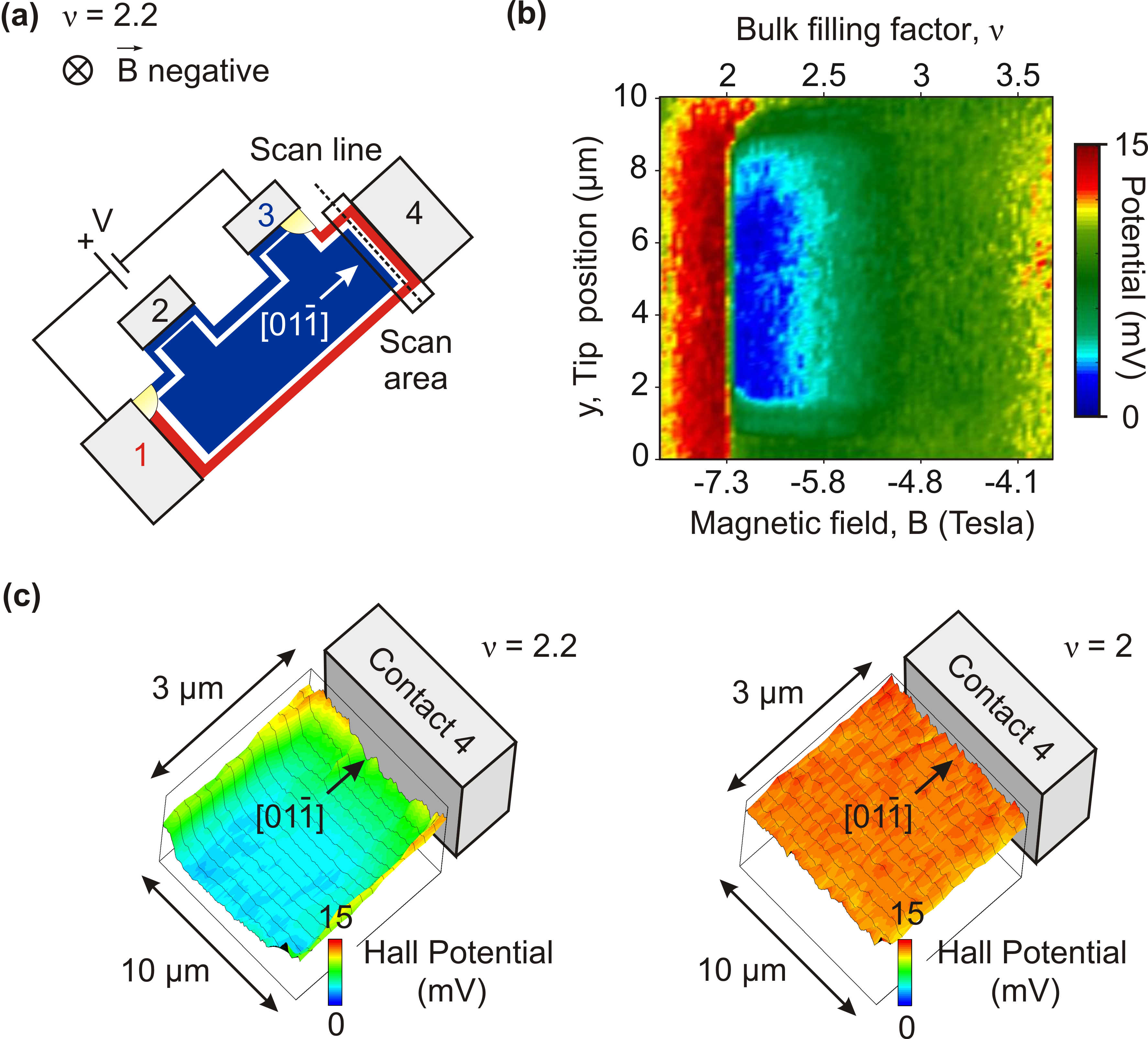
In Fig. 3 the potential profiles correspond to the measurement configuration . For a negative magnetic field between and , the potential drops at the upper mesa side from the edge to the bulk, remains constant over the bulk and drops towards the lower mesa side to increase again at the edge. This unusual potential profile is observed for almost the complete magnetic field range. Obviously, the current driven between contact 1 and 2 runs along the whole edge of the sample passing by contact 3 and 4. Indeed, a non-local resistance has been found for negative magnetic field. For positive fields, no resistance is detected and consistently, the related potential distribution given in Fig. 3b shows a constant potential from upper to lower mesa side, i.e. no current passing forth and back through this cross section. As indicated in Fig. 3b, a decoupling of the bulk and the contacts 1 and 4 is required to explain the presence of non-local resistances. Fig. 4 presents the potential distribution in the vicinity of contact 4 for the measurement arrangement . It directly proofs the decoupling by an incompressible strip at : The potential of the compressible bulk is low even thus the surrounding edge regions on the lower mesa side, in front of the contact 4 and at the upper mesa side are high in potential.
 |
In summary, by comparing magneto transport and scanning probe investigations, we could identify that the presence of an incompressible strip in front of state-of-the-art ohmic contacts might cause an electrical decoupling of the compressible 2DES bulk region from the contacts. Important, we discover that the insulating properties of this incompressible strip depend on the orientation of the interface line 2DES/alloyed contact relatively to the underlying (Al,Ga)As/GaAs heterostructure. A contact with its interface line perpendicular to [011] equilibrates the compressible bulk and edge, whereas at the same time contacts with the interface line perpendicular to [01-1] does not. This anisotropy is related to different electron density profile at the contact interface which determines in high magnetic field the incompressible strip thickness. Adiabatic transport features hence originates in high electron mobility Hall bar with a geometry having contacts arranged on only three of four sides of the mesa. We conclude, non-ideal (ideal) contact behaviour in terms of the Landauer-Büttiker formalism can be attributed to a smooth (sharp), partial electrostatic depletion in front of ohmic contacts allowing for an large (thin) isolating incompressible strip.
Acknowledgements.
The authors thank M. Riek and T. Reindl for sample processing help, O. Göktas and Y. Boss for their collaboration in study alloyed contact properties, and A. Siddiki, R.R. Gerhardts, D. Quirion and A.C. Welker for discussions. The 2DES wafer was provided by W. Wegschneider. We acknowledge the Deutsche Forschnungsgemeinschaft (DFG) for financial support under WE 1902/1.References
- (1) K. McCormick, M. Woodside, M. Huang, M. Wu, P. McEuen, C. Duruoz, and J. Harris, Phys. Rev. B 59, 4654 (1999)
- (2) P. Weitz, E. Ahlswede, J. Weis, K. Klitzing, and K. Eberl, Physica E 6, 247 (2000)
- (3) E. Ahlswede, P. Weitz, J. Weis, K. Klitzing, and K. Eberl, Physica B 298, 562 (2001)
- (4) E. Ahlswede, P. Weitz, J. Weis, K. Klitzing, and K. Eberl, Physica E 12, 165 (2002)
- (5) D. Chklovskii, B. Shklovskii, and L. Glazman, Phys. Rev. B 46, 4026 (1992)
- (6) K. Lier and R. Gerhardts, Phys. Rev. B 50, 7757 (1994)
- (7) A. Siddiki and R. Gerhardts, Phys. Rev. B 68, 125315 (2003)
- (8) A. Siddiki and R. Gerhardts, Phys. Rev. B 70, 195335 (2004)
- (9) M. Büttiker, Phys. Rev. B 38, 9375 (1988)
- (10) A. Roth, C. Brüne, H. Buhmann, L. Molenkamp, J. Maciejko, X. Qi, and S. Zhang, Science 325, 294 (2009)
- (11) M. Büttiker, Science 325, 278 (2009)
- (12) In controlled experiments, ’ideal and non-ideal’ contact properties are mimiced by locally depleting the 2DES by gate electrodes in front of contacts.
- (13) R. Haug, Semicond. Sci. Technol. 8, 131 (1993)
- (14) H. van Houten and C. Beenakker, Solid State Physics 44, 1 (1991)
- (15) S. Komiyama and H. Nii, Physica B 184, 7 (1993)
- (16) B. Alphenaar, P. McEuen, R. Wheeler, and R. Sacks, Phys. Rev. Lett. 64, 677 (1990)
- (17) P. McEuen, A. Szafer, C. Richter, B. Alphenaar, J. Jain, A. Stone, R. Wheeler, and R. Sacks, Phys. Rev. Lett. 64, 2062 (1990)
- (18) B. van Wees, E. Willems, L. P. Kouwenhoven, C. Harmans, J. Williamson, C. Foxon, and J. Harris, Phys. Rev. B 39, 8066 (1989)
- (19) O. Goktas, J. Weber, J. Weis, and K. Klitzing, Physica E 40, 1579 (2008)
- (20) M. Kamada, T. Suzuki, F. Nakamura, Y. Mori, and M. Arai, Appl. Phys. Lett. 49, 1263 (1986)
- (21) The filling factor is obtained from the electron density and magnetic field by .
- (22) C. Uiberacker, C. Stecher, and J. Oswald, Phys. Rev. B 80, 235331 (2009)
- (23) P. Weitz, E. Ahlswede, J. Weis, K. Klitzing, and K. Eberl, Appl. Surf. Sci. 157, 349 (2000)
- (24) M. Woodside, C. Valea, K. McCormick, P. McEuen, C. Kadow, K. D. Maranowski, and A. C. Gossard, Physica E 6, 238 (2000)
- (25) The current is hence concentrated in a region of carrier density smaller than the bulk density as it was expected from the shift of Hall plateaus to lower magnetic fields.