Physics of interface: Mott insulator barrier sandwiched between two metallic planes
Abstract
We consider a heterostructure of a metal and a barrier with onsite correlation at half filling using unrestricted Hartree Fock. We find that above a certain value of correlation strength in the barrier planes, the system is a Mott insulator, while below this value the system still behaves like a gapless insulator. The energy spectrum is found to be very novel with the presence of multiple gaps. Thus the system remains non metallic for any finite value of correlation.
pacs:
73.20.-r, 71.27.+a, 71.30.+h, 71.10.Fd, 73.21.b, 73.40.cI Introduction
Recently there has been a spurt in the study of multilayered heterostructures, fabricated out of strongly correlated materials. A wide range of systems have been studied experimentally and theoreticallyOhtomo ; Thiel ; Lee ; Kancharla ; Okamoto ; Rosch ; Krish . The interface of a band insulator and a Mott insulators can show metallic behavior Ohtomo or can even become superconducting Thiel . As shown by Thiel et al., such interfaces can be manipulated by gate voltages thereby opening the prospect for interesting novel devices.
In this letter, we investigate the interface of a metal and a system with finite onsite correlation. For onsite correlation greater than a certain value the system opens a gap, which mimics the Mott insulator. What happens when we sandwich this system between two metallic planes? We find that the overall system behaves as an insulator not only in the region where there is a gap but also in the region where the system is gapless.
The introduction of metallic planes induces multiple gaps in the energy spectrum for high values of onsite correlation . This can be understood to be due to the emergence of vastly different types of sites both in plane and perpendicular to it. The gapless region behaves as a disordered insulator, with the disorder coming from the induced inhomogenity in the underlying Coulomb landscape. There is a charge reconstruction across the planes for such a system as we vary . In the region of parameters where a gap opens up, this reconstruction is more vigorous.
The interface that we have studied has been studied by othersRosch ; Krish using inhomogeneous dynamical mean field theoryGeorges ; Metzner ; Potthoff ; freericks_idmft . However, in the IDMFT approach used above all sites in each of the planes are treated as identical(spatial variation is taken only along the z direction), and thus misses out on crucial in plane modulations, which is one of the crucial reasons for the opening up of multiple gaps in the spectrum. It also considers a paramagnetic solution for the magnetic sector, which is not the correct solution for an underlying cubic lattice that we study.
We employ the method of unrestricted Hartree Fock to solve the problem. It can capture the physics arising due to spatial variations both in and perpendicular to planes. It can handle the charge and magnetic sector on the same footing and treats correlations in a self consistent fashion. Recently we have shown the utility of this method in describing the metallic phase that arises in two dimensions as a result of competition between correlation and disorderNandini ; Gupta .
I.1 Model and Method
The barrier planes are described by the single orbital Hubbard model and the metallic planes by the non interacting tight-binding model. The Hamiltonian for the system is
| (1) | |||||
Here the label indexes the planes, and the label indexes sites of the two-dimensional square lattice in each plane. The operator () creates (destroys) an electron of spin at site on the plane . We set the in-plane hopping to be nearest neighbor only, and equal to , the hopping between planes, so that the lattice structure is that of a simple cubic lattice. We take for the barrier planes, and zero for the metallic planes. The chemical potential is calculated by demanding that there be exactly N electrons in the problem. This is done by taking the average of the N/2 th and the N/2 + 1 th energy level. We make no further assumption about the magnetic regime, and thus retain all spin indices in the formulas below. We label the barrier planes with values from 1 to m. Thus correspond to the metallic layers and all the other values correspond to the barrier planes.
|
|
|
|
|
|
I.2 Calculated quantities
The energy spectrum of the system is very rich, with the presence of multiple gaps in it. We have also calculated the charge profile, spin profile and the dc conductivity at zero temperature. We calculate the effect of correlations and layer variation on the multiple gaps. The value of charge and spin at a particular site in the central square of each plane is taken and is plotted against the plane index to clearly bring out the inhomogeneous profile along the direction. The charge at a particular site is simply calculated as = + . The spin at a particular site is given by = . The dc conductivity is calculated using the Kubo formula, which at any temperature is given by:
| (2) |
with , being the lattice spacing, and = Fermi function with energy . The are matrix elements of the current operator , between exact single particle eigenstates , , etc, and , are the corresponding eigenvalues. In this paper, conductivity/conductance is expressed in units of .
We calculate the ‘average’ conductivity over small frequency intervals, ( = , n = 1,2,3,4), and then differentiate the integrated conductivity to get at , n = 1,2,3SanjeevEPL . We repeat the same calculation for each temperature slice upto The temperature dependence of the conductivity tells us about the underlying nature of the overall system.
For the quasi 2D geometry taken by us , where is the total number of layers and L is the total number of sites along both x and y direction, in the numerical work. We have performed finite size scaling of each of our results. We have shown the result of finite size scaling on the dc conductivity for a particular parameter set() in this paper due to paucity of space. The effect of varying the number of Mott layers has been studied in great detail in this paper.
|
|
I.3 Our Work and Results
We have calculated the dc conductivity , within the accuracy allowed by these finite size systems. The conductivity is calculated in units of the universal conductance . Our method is able to capture the phenomenon of the gap opening as goes above a certain threshold. We find two types of insulators, one is gapped and the other is not. This second type of insulating behaviour which is shown for low , , ( is the value of above which the system opens up a gap), is a disordered insulator, where the disorder is introduced by the introduction of the metal interfaces at the bottom and top.
The effect of varying the insulating layer thickness on the charge order and spin order profile has been studied in this work. As the gap at half filling closes the spin order parameter collapses to near zero values. The charge order parameter on the other hand varies less dramatically across the gap closing transition. The charge profile builds up to its maximum value at the metallic planes and then dips to their lowest values in the first adjacent planes, from where there is massive charge depletion to the metallic planes, to gain Coulomb energy. As we move vertically deeper into the Mott planes, the total charge again picks up, reaching its bulk maxima at the central layer. There is overall symmetry around the central plane, as expected. As we increase the bulk thickness, we find that the charge peak at the central plane slowly approaches the value without the metallic planes, which is unity. This clearly indicates that the bulk becomes gradually insensitive to the metallic planes at the surfaces, as we increase the bulk layer thickness.
|
|
|
|
I.4 Analysis of our results
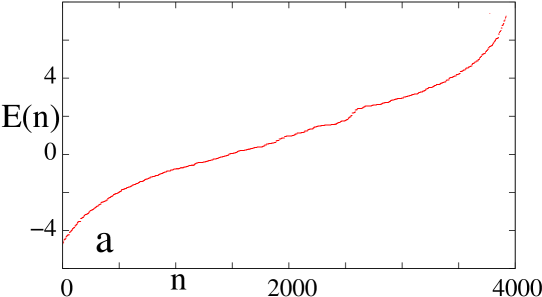
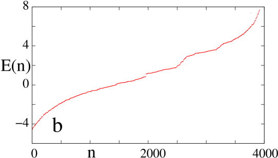
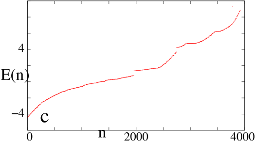
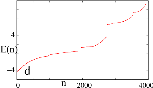
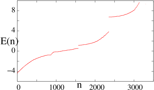
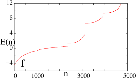
The sites having higher energy will have lower occupation and vice versa. Fig 1a,b,c,d,e and f shows that different types of sites emerge in the problem that we study, as we systematically increase . For different values of , these gaps will open up successively. For , which means 3 intervening Mott layers, the first gap opens up roughly between and , the second gap opens up close to and the third gap opens up close to . The presence of 3 gaps clearly indicates the presence of broadly 4 different types of sites for .
The 4 different types of sites correspond to the following. The first gap exactly at half filling corresponds to the situation when the has become large enough to just introduce some anti ferromagnetic ordering(however weak) even in the metallic planes. Thus the overall system develops a rather inhomogeneous Neel ordering, where the inhomogeneity is along the z direction. Another way of looking at it is to say that in the absence of metallic planes, there would be a big gap at half filling. The introduction of metallic planes reduces this gap to a somewhat lower value. As a result of this induction of anti ferromagnetic ordering(this will be discussed in more details while explaining our spin/charge order results), two different types of sites emerge in the metallic plane for either spin. The reason for the generation of these two different type of sites in the metallic planes is as follows.
To consider the emergence of two distinct types of sites due to the presence of interface, let us look at a particular spin(up/down). In the first type, an up electron sees comparatively high density of up spin and low density of down spin in the adjacent site in the Mott plane. Such an up electron will experience lower Hubbard repulsion and greater Pauli blocking if it wants to hop to the adjacent site in the Mott plane. An up electron in the second type of site sees comparatively lower up electron density and higher down spin density in the adjacent site on the Mott plane. This will lead to the second type of up electron experiencing higher Hubbard repulsion and lower Pauli blocking if it wants to gain kinetic energy by hopping to the adjacent Mott plane.
As we increase to about 7, the energy band of the electrons in the Mott planes decouple completely from the energy band of the electrons in the metallic planes, thus creating the second gap in the spectrum. The Mott layers now form the topmost band. As we crank up the further, the environment seen by the sites in the Mott planes gets split further. An electron located in the central plane/s has the strongest Neel order, while an electron located in the the Mott layers adjacent to the metallic planes have a relatively weaker Neel order. With increasing the central layer becomes distinct from the two Mott layers which are adjacent to the metallic planes. This leads to the further splitting of the uppermost band at around . In Fig. 1e for system size , the uppermost gap is absent because of non existence of the central layer.
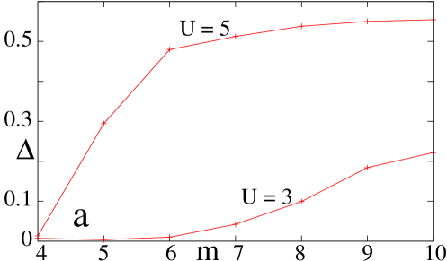
Fig. 2a shows the plot of the gap at half filling as we increase the number of Mott layers for and 5. It shows that for m = 4 and 5 there is no gap at half filling till . The gap opens up when .
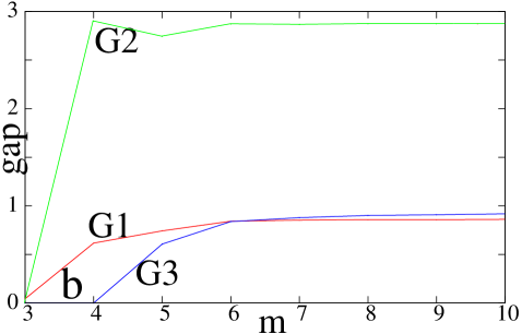
Fig.2b shows how the multiple gaps in the energy spectrum () behaves on increasing the number of Mott layers for . This is because on increasing the width the number of sites at which the electron encounters will rise, so the barrier becomes stiffer.
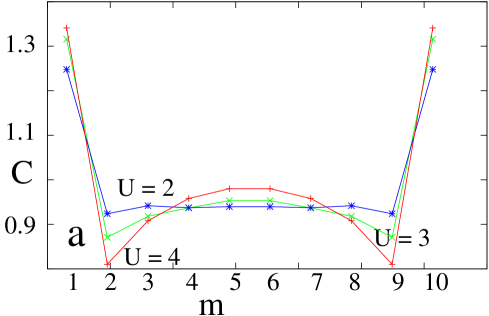
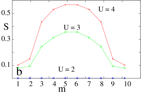
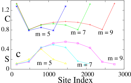
Fig 3a shows the plots of total charge at a particular point in the central square of each layer vs the layer index for , for three different values of . We can see clearly how as increases the charge profile in the Mott layers become more and more non uniform along the z direction, thus developing a more pronounced hump. The charge depletion from the Mott layers just adjacent to the metallic planes and the the charge accumulation in the metallic planes increases with increasing . In Fig 3b we have shown the plot of vs layer index for and = 2,3,4. While is almost zero and featureless for , it starts showing a prominent feature which gets sharper as is increased to 3 and then 4. Fig 3c shows the plots of and for but for three different values of . As we increase the number of Mott layers, for a fixed , becomes more pronounced, while becomes more asymmetric in terms of increasing difference between the value in the central Mott plane and the Mott plane adjacent to the metal planes.
|
|
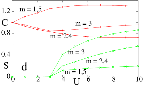
In Fig 3d we show the plot of and vs for system. We have gone from = 0 to = 10 in integral steps. It clearly shows the emergence of three grossly different types of planes as we increase . The three different types of planes are a) the two metallic planes, b) the two Mott planes adjacent to the metallic planes and c) the remaining Mott plane/s. We can see that as we increase , more charge accumulates on the metallic planes and there is acute charge depletion from Mott planes adjacent to the metallic planes. There is charge depletion from central Mott plane/s also initially, but as we increase further, the charge at the central Mott plane/planes increases slightly. This is accompanied by a large anti ferromagnetic ordering in the central planes/s. Thus the charges in the central Mott plane/s are unable to delocalize as it faces strong Coulomb repulsion on all sides and thus it piles up.
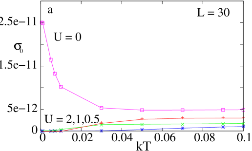
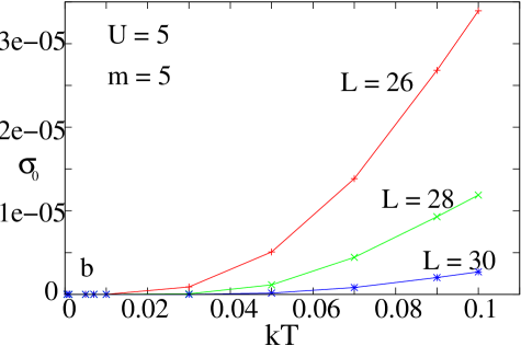
In Fig. 4a we show the plots of dc conductivity against temperature for = 0,0.5,1 and 2 for a system, which is the largest system size that we have considered. The has been chosen to be twice the finite size spacing between energy levels for each of the system size that we have considered. The dc conductivity curve for , shows metallic behaviour as expected with a sharply falling profile with increasing . We note that the value of conductivity obtained for the metal is severely suppressed. This is because, the highest contribution for the metal is at , which cannot be sampled in our finite size simulation. Thus we are able to sample the at some low but finite where the conductivity has already fallen very sharply. As we increase the dc conductivity for low gets severely suppressed by several orders of magnitude and the system is an insulator even for . This is due to the emergence of significant amount of inhomogeneity in the charge density landscape at . As we increase further, the amount of induced disorder increases further, suppressing conductivity even further. For , a small gap at half filling opens up, which seperates the occupied and unoccupied states. Fig 4b shows the finite size scaling effect on the vs curves for , where we have taken = 26,28,30, all of which show insulating behaviour. We have convinced ourselves that the result of finite size scaling on the gap at half filling, converges to a fixed value for for . We find very high thermally activated conductivity which increases by several orders of magnitude.
II Conclusion
A heterostructure system arising due to the sandwich of a barrier with finite width and onsite correlations between two metallic planes is studied. There are multiple gaps in the spectrum, with increasing . An inhomogeneous spin and charge profile develops in the system. Dc conductivity calculations have been performed showing that the system is an insulator both in the gapped and gapless region.
III Acknowledgement
Sanjay Gupta would like to thank the DST for providing the grant under the project ”Electronic states and transport in mesoscopic/nanoscopic systems”.
References
- (1) A. Ohtomo et al., Nature (London), 419, 378 (2002), Nature (London), 427, 423 (2004).
- (2) S. Thiel et al., Science, 313, 1942 (2006).
- (3) W. C. Lee and A. H. MacDonald, Phys. Rev. B,74, 075106 (2006).
- (4) S. S. Kancharla and E. Dagotto,Phys. Rev. B,74, 195427 (2006).
- (5) S. Okamoto and A. J. Millis, Nature (London),428, 630 (2004); Phys. Rev. B, 70, 241104(R) (2004); Phys. Rev. B,72, 235108 (2005).
- (6) R. W. Helmes, T. A. Costi, and A. Rosch, Phys. Rev. Lett. 101, 066802 (2008).
- (7) H. Zenia, J. K. Freericks, H. R. Krishnamurthy, Th. Pruschke , Phys. Rev. Lett., 103, 116402, (2009).
- (8) A. Georges, G. Kotliar, W. Krauth, and M. J. Rozenberg, Reviews of Modern Physics, 68, 13 (1996).
- (9) W. Metzner and D. Vollhardt, Phys. Rev. Lett., 62, 324 (1989).
- (10) M. Potthoff and W. Nolting, Phys. Rev., B 59, 2549 (1999); S. Schwieger, M. Potthoff, and W. Nolting, ibid. 67, 165408 (2003).
- (11) J. K. Freericks, Phys. Rev. B 70, 195342 (2004).
- (12) Dariush Heidarian and Nandini Trivedi, Phys. Rev. Lett.,93,126401
- (13) Tribikram Gupta and Sanjay Gupta, Euro Physics Letters 88, 17006 (2009)
- (14) Sanjeev Kumar and Pinaki Majumdar, Europhys. Lett 65, 75 (2004)