Bulk band gap and surface state conduction observed in voltage-tuned crystals of the topological insulator Bi2Se3
Abstract
We report a transport study of exfoliated few monolayer crystals of topological insulator Bi2Se3 in an electric field effect (EFE) geometry. By doping the bulk crystals with Ca, we are able to fabricate devices with sufficiently low bulk carrier density to change the sign of the Hall density with the gate voltage . We find that the temperature and magnetic field dependent transport properties in the vicinity of this can be explained by a bulk channel with activation gap of approximately 50 meV and a relatively high mobility metallic channel that dominates at low . The conductance (approximately 2 7), weak anti-localization, and metallic resistance-temperature profile of the latter lead us to identify it with the protected surface state. The relative smallness of the observed gap implies limitations for EFE topological insulator devices at room temperature.
pacs:
73.20.-r, 73.20.Fz, 73.23.-b, 73.63.-bTopological insulators (TIs) are a new phase of matter which is electrically insulating in the bulk but has unusual conducting surface states (SS) Fu07 ; Moore07 ; Bernevig06 ; FuKane07 ; QiHughes08 . The SS are spin polarized, protected from scattering by non-magnetic impurities, and have an approximately linear energy-momentum dispersion at low energy. These properties make them relevant for applications ranging from improved spintronic devices to producing analogs of exotic high energy particles potentially useful for quantum computing HasanReview . Particular interest has been focused on 3D TIs based on Bi, where the topologically non-trivial surface 2D electron gas has been positively identified by angle-resolved photoemission spectroscopy (ARPES) in Bi-Sb Hsieh08 , Bi2Se3 Xia09 , and Bi2Te3 Shen09 . Proposals for realizing devices that harness the aforementioned properties of the SS most often involve electrical transport FuKane09 ; FuKane09b ; Akhmerov09 ; Franz09 ; Linder10 . Thus far, characterizing or even identifying the SS in such experiments has proven difficult. Because transport is a bulk sensitive measurement, even a small conductivity from imperfections in the bulk overwhelms the surface contribution because of the geometric advantage of the former. The materials obstactles to placing the chemical potential in the bulk band gap of the TI are at present the most serious obstacle to realizing TI devices.

Recent measurements in high magnetic fields have identified the surface state as a parallel conductance channel with the bulk oblig1 ; oblig2 ; oblig3 . Several experiments have been recently undertaken to circumvent the bulk contribution to transport in TIs by preparing Bi2Se3 in thin film form Chen10 ; MIT ; Kong10 ; Minhao10 . However, in both bulk crystals and nanocrystals of Bi2Se3, is usually pinned to the conduction band (CB) due to the presence of Se vacancies Hyde74 ; MIT . This large remnant electron density is too large to remove by the electrostatic gating techniques available for thin films. Thus, while thin film experiments have been able to show signs of surface phenomena, namely remnants of weak anti-localization Chen10 ; Minhao10 , basic transport properties of TIs have remained elusive as the bulk carriers cannot be effectively removed.
Here we report experiments on Ca passivated crystals of Bi2Se3 in a field effect transistor device that allow us to successfully suppress the bulk states and investigate the transport properties of the SS. We mechanically exfoliated crystals of Ca doped Bi2Se3 (up to 0.5% substituted for Bi) onto doped silicon wafers coated with 300 nm SiO2. The Ca doping results in hole doped bulk crystals Hor09 ; Check09 , which after fabrication of contacts via e-beam lithography (Cr/Au) in the Hall geometry have relatively close to the bulk band gap on the CB side. In samples with uniform thickness , a negative larger than -150 V can be applied without triggering breakdown. For 10 nm, from electrostatic arguments this suffices to move deep into the gap for bulk carrier densities 1018 - 1019 cm-3.
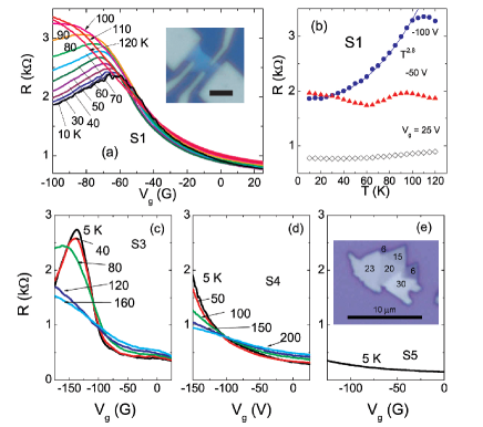
The use of 300 nm SiO2 allows optical identification of thin crystals. It was found that for crystals thinner than 30 nm the observed color of the cleaved crystals darkens toward the color of the substrate. This is similar to what has been found in graphene and other 2D crystals Geim04 . Cross correlating the optical images with atomic force microscope (AFM) images, we were able to generate a mapping between color and thickness useful for identifying thin crystals optically within an approximate thickness 2 nm. An optical image of a crystal with varying thickness measured by both AFM and optical microscopy is shown in the inset of Fig 1e. We study crystals down to 5 nm; ARPES experiments on thin films of Bi2Se3 have shown the SS persist to this thickness arpesThin .
Table 1 shows parameters for five different devices. Devices of thickness nm exhibit similar characteristics. For these devices an applied gate voltage can change the Hall response from electron-like to hole-like at the neutral voltage . Each exhibits a maximum at low in the resistance per square of k, as shown for samples S1 and S3 in Fig. 1a and 1c, respectively. For thicker crystals such as devices S4 and S5, we reach the threshold for breakdown of the SiO2 gate dielectric (typically -180 V to -200 V) without observing such a peak (see Fig. 1d and 1e). The progressively thicker crystals show systematically less response to the applied gate voltage. It is found that the act of cleaving and device fabrication reduces the carrier mobility and increases the electron density. Device S5 (see Fig. 1e and Table I) has a 0.3 K mobility approximately 1090 cm2 V-1s-1 with 6 1018 e- cm-3 was cleaved from a bulk crystal measured to have a mobility 7000 cm2 V-1s-1 with 2 1018 e- cm-3. It is unclear if the cleaving process or lithographic process is responsible for this degradation. From here we focus on the results of samples S1 and S2.
| units | nm | V | cmVs | k |
|---|---|---|---|---|
| S1 | 10 2 | -80 | 330 | 2.4 |
| S2 | 6 2 | -90 | 830 | 2.3 |
| S3 | 20 4 | -170 | 720 | 2.8 |
| S4 | 30 5 | -175 | 910 | 1.9 |
| S5 | -175 | 1090 | 0.3 |
Figure 1a displays traces of the zero-field resistance vs. at selected from 10 to 120 K (sample S1). For -55 V, is nearly independent, characteristic of a bad metal in which disorder scattering is dominant (Fig. 1b). Surprisingly, if is tuned lower ( -55 V), displays a power-law variation (=2.8) that extends to 110 K, where displays a broad maximum. We show below (Eq. 1) that both the gate-induced transformation (from a -independent to one with power-law variation) and the existence of the broad peak in are accounted for by a 2-band model comprised of a bulk band in parallel with a surface channel with higher mobility at this large negative gate voltage. When is near -55 V, appears to be at the CB band edge.

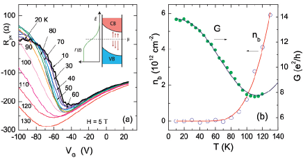
The Hall resistance confirms that the carriers are -type for -55 V (Fig. 2a). is independent, consistent with a bulk metal. Additionally, is linear as we would expect from a simple electron band being emptied by the gate (induced charge , where the capacitance per unit area of the gate dielectric). As is lowered below -55 V, the curves of vs. display a strong dependence on . Below 30 K, changes sign near = -80 V. We can understand this in terms of moving below the SS Dirac point or near the VB edge. It is important to note that the gating does not rigidly shift in the device. For samples with (the depletion length), the bands are strongly bent upwards when is large and negative (inset in Fig. 2a). As is grounded at the drain, it falls within the gap inside the crystal. While the specific shape of the bending is difficult to calculate, we can adopt the most simple limit by treating the system as a metal - (doped) semiconductor interface in the full depletion approximation. The Poisson equation for the potential , charge density (estimated as 1019 e- cm-3 from ), and dielectric constant as a function of the distance from the interface is then . The curvature of the band is that depicted in Fig. 2a for a 10 nm crystal that should be preserved in more realistic calculations, which will be important for analyzing the role of thermally activated carriers.
We assume that, when is inside the gap, the observed conductance is the parallel combination
| (1) |
where is the surface conductance, with the two-dimensional (2D) density and the mobility ( is the electron charge and = 2.8). To account for disorder scattering, we write , and treat the zero- surface conductance and as adjustable parameters. The second term is a bulk conductance resulting from thermal excitation of carriers into the CB described by the density (arrows in inset, Fig. 2a). The mobility at the bottom of the CB is taken to be a constant (disorder-scattering dominant). We note that, in addition to originally being in the CB, the curvature of the band bending in the case of a remnant electron pocket favors excitation in to the CB for devices of finite . Integrating the excited carriers ( is the energy difference between the VB and CB band edges and ) , we can expect the electron-like carriers to dominate due to the direction of the band bending.
Equation 1 gives a good fit to vs. (Fig. 2b). From the fit, we obtain = 13.9 ( = 2.5 10-6). This implies a conductance of approximately 7 per surface. As increases from 10 K, inelastic scattering strongly reduces . Meanwhile, excitation across the gap = 53030 K leads to a rapid growth in the bulk . This reverses the decreasing trend of at 110 K, as shown in Fig. 1b. At 130 K, the 2 terms, = 3.65 and = 4.5 , become roughly comparable. Thus, we show that despite the large intrinsic gap in Bi2Se3 (300 meV), we must go below 100 K for the device to be dominated by surface conduction. One likely origin of this reduction in energy gap is the band bending depicted in Fig. 2a, which effictively narrows the gap upon increased gating. This implies limitations for accessing the SS at room temperature.
To measure more accurately, we turn to the Hall results in Fig. 2a. We may obtain by studying how depends on both and when is in the gap. At the lowest (bold curve at 10 K), is at the zero-crossing when = -80 V. As is raised with fixed, the balance condition is unaffected until 80 K, whereupon swings to negative values, with the thermal activation of carriers into the CB. However, the balance point can be restored if is made more negative to draw more holes into the crystal (e.g., -98 V at 100 K). From the gate-shift needed at each , we calculate the activated density as . A fit to yields a gap of 640 K (Fig. 2b). This excitation supports the band bending proposed in Fig. 2a. Combining the value cm-2 at 130 K with the value of inferred from Eq. 1, we obtain the mobility 147 cm2/Vs (at the bottom of the CB).
Hence, the gate-driven transformation to a conductor with strong dependence in both and is explained quantitatively as the opening of a small gap 50 meV between and the CB. Depletion of the CB carriers exposes a high-mobility channel . The possibility that this channel is a bulk impurity band can be excluded because electrons therein generally have even lower mobilities (1-10 cm2/Vs) than obtained for .

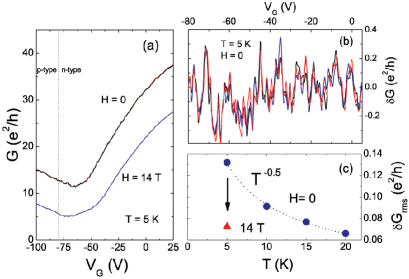
The enhanced mobility for is confirmed by the transverse magnetoresistance (MR). Fig 3a compares the zero-field conductance at 5 K with the conductance measured in with at 14 T as a function of (we suppress in hereon). The semi-classical MR expression may be used to determine the average mobility . At 20 V ( in the CB), the reduction in by 25 gives 380 cm2/Vs, consistent with the Hall analysis (see Table I). The larger reduction () in the gap region (-80 V) gives = 850 cm2/Vs, which we identify with . From , we can estimate 1012 cm-2 at V.

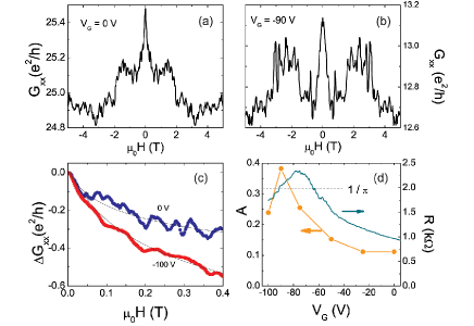
At low , fluctuations in are observed if or is swept. Fig. 3b displays the trace of fluctuating component vs. , where is a smooth background. The amplitude of is nominally uniform over the entire range V. The amplitude (Fig. 3c) follows a scaling consistent with a 2D electron system with a dephasing length smaller than the system size Lee87 . Recent observation of reproducible fine structure driven by in both transport and STM measurements have been reported Check09 ; Hanaguri10 . Here, for = 0 (Fig. 4a), we observe in Sample S2 () shown in Fig. 4d) a sharp, narrow peak at = 0 flanked by mesa-like structures in addition to the fluctuations. However, the large amplitude fluctuations (rms amplitude up to 6) that we found in bulk samples of the same material previously Check09 do not survive in these exfoliated devices. The reason for this and the origin of the detailed structures observed (including the suppression by shown in Fig. 3c) deserve further study.
The sharp anomaly in at = 0 in Figs. 4a and 4b is consistent with the quantum correction arising from anti-localization given by Hikami
| (2) |
where is the dephasing magnetic field, is the digamma function, and the parameter is positive for antilocalization. If spin-orbit coupling is strong, theory predicts Hikami , or if we have 2 surfaces, as here. Confining the fit to fields below 0.4 T, we show 2 traces in Fig. 4c at = 0 and -100 V. Fits across the full range of are shown in Figure 4d. At , peaks at 0.38, which is within 20% of the expected value . Reports of similar experiments on epitaxially grown films report approximately half of this value, consistent with one surface state Chen10 ; Minhao10 . We hypothesize the disparity may arise from the different nature of the strained interface of the epitaxial films and the exfoliated crystal here. We also find a peak in the dephasing field close to indicating a reduction in the dephasing length from 220 nm at zero to 67 nm at -90 V. The value at zero gate is consistent with those reported in epitaxial films of similar thickness Minhao10 , while the reduction in has been suggested as evidence for reduced screening and increased electron-electron interaction effects in the low density regime Chen10 . The observation of along with the sign change in , supports our main conclusion that, at , is well inside the bulk band gap. Notably, even with in the CB, a signature of weak anti-localization persists.
Electrostatic control of provides a powerful means for comparing the bulk and surface conductances in chemically doped TIs. We anticipate that replacing the Au electrodes with magnetic or superconducting materials will enable us to probe exotic states that have been proposed FuKane09 ; FuKane09b ; Akhmerov09 ; Linder10 ; Franz09 . The current devices allow access to surface dominated transport for these experiments below 100 K.
We acknowledge support from the U.S. National Science Foundation (NSF DMR 0819860). † Present address: Advanced Science Inst, RIKEN, Saitama, Japan 351-0198. ‡ Present address: Dept of Physics, Missouri Inst of Science and Technology, Rolla, MO 65409, USA.
References
- (1) L. Fu, C. L. Kane, E. J. Mele, Phys. Rev. Lett. 98, 106803 (2007).
- (2) J. Moore, L. Balents, Phys. Rev. B75, 121306(R) (2007).
- (3) B. A. Bernevig, S. C. Zhang, Phys. Rev. Lett. 96, 106802 (2006).
- (4) L. Fu, C. L. Kane, Phys. Rev. B76, 045302 (2007).
- (5) X.L. Qi, T.L. Hughes, S. C. Zhang, Phys. Rev. B78, 195424 (2008).
- (6) For a review, see M. Z. Hasan and C. L. Kane, Rev. Mod. Phys. 82, 3045 (2010).
- (7) D. Hsieh et al., Nature 452, 970 (2008).
- (8) Y. Xia et al., Nature Phys 5, 398 (2009).
- (9) Y. L. Chen et al., Science 325, 178 (2009).
- (10) L. Fu and C. L. Kane, Phys. Rev. Lett. 102, 216403 (2009).
- (11) L. Fu and C. L. Kane, Phys. Rev. B 79, 161408(R) (2009).
- (12) A. R. Akhmerov, Johan Nilsson, and C. W. J. Beenakker, Phys. Rev. Lett. 102, 216404 (2009).
- (13) B. Seradjeh, J. E. Moore, & M. Franz, Phys. Rev. Lett. 103, 066402 (2009).
- (14) J. Linder et al., Phys. Rev. Lett. 104, 067001 (2010).
- (15) D. Qu, Y. S. Hor, J. Xiong, R. J. Cava, and N. P. Ong, Science 329, 821 (2010).
- (16) J. G. Analytis et al., Nature Physics 6, 960 (2010).
- (17) Z. Ren et al., Phys. Rev. B 82, 241306 (2010).
- (18) J. Chen et al., Phys. Rev. Lett. 105, 176602 (2010).
- (19) H. Steinberg, D. R. Gardner, Y. S. Lee, and P. Jarillo-Herrero, Nano Lett. DOI: 10.1021/nl1032183 (2010).
- (20) D. Kong et al., Nano Lett. 6, 2245 (2010).
- (21) M. Liu et al., arXiv:1011.1055 (2010).
- (22) G. R. Hydeet al., J. Phys. Chem. Solids 35, 1719 (1974).
- (23) Y.S. Hor et al., Phys. Rev. B79, 195208 (2009).
- (24) J. Checkelsky et al., Phys. Rev. Lett. 103, 246601 (2009).
- (25) K. S. Novoselov et al., Proc. Nat. Acad. Sci. 102, 10451-10453 (2005).
- (26) Y. Zhang et al., Nat. Physics 6, 584 (2010).
- (27) P. A. Lee, A. D. Stone, and H. Fukuyama, Phys. Rev. B 35, 1039 (1987).
- (28) T. Hanaguri et al., Phys. Rev. B 82, 081305(R) (2010).
- (29) S. Hikami, A. I. Larkin, Y. Nagaoka, Prog. Theor. Phys. 63, 707 (1980).