A Two-Dimensional Carbon Semiconductor
Abstract
We show that patterned defects can be used to disrupt the sub-lattice symmetry of graphene so as to open up a band gap. This way of modifying graphene’s electronic structure does not rely on external agencies, the addition of new elements or special boundaries. The method is used to predict a planar, low energy, graphene allotrope with a band gap of 1.2 eV. This defect engineering also allows semiconducting ribbons of carbon to be fabricated within graphene. Linear arrangements of defects lead to naturally embedded ribbons of the semiconducting material in graphene, offering the prospect of two-dimensional circuit logic composed entirely of carbon.
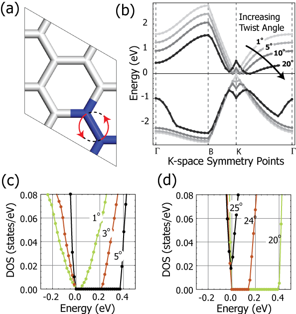
Graphene-based electronics promise to overcome limitations associated with silicon technologies ref:Novoselov2007 ; ref:geim-the-rise-of-graphene ; ref:Bolotin2008 ; ref:Lin2010 and open previously unavailable new applications ref:Schedin2007 . The improved performance derives from unparalleled strength ref:Lee2008 combined with high electron mobility ref:Novoselov2005nature ; ref:Bolotin2008 . Graphene is a semi-metal, though, and therefore requires modification to open up the band gap desirable for logic circuits. This is simple to do in principle, as demonstrated in Figure 1, where small rotations of a bond, periodically repeated through the lattice, collapses the Dirac cones at the graphene K point. Continued rotation of the bond will close the band gap elsewhere resulting in a conductor. To exploit this sensitivity, an agency must be found for tuning the distortion of lattice symmetry.
A number of approaches have been considered for distorting graphene so that it exhibits a band gap. All of these rely on either the action of an external agency or a confining boundary to disrupt the delicate sub-lattice symmetry. These include the use of strongly interacting substrates ref:Ohta2006 ; ref:Giovannetti2007 ; ref:Ciobanu2009 or the application of electric fields in graphene bi-layers ref:Ohta2006 ; ref:zhang2005 ; ref:Nilsson2007 . Quantum confinement effects can also be exploited as in carbon nano-ribbons ref:Brey2006 ; ref:Mucciolo2009 ; ref:Hod2007 ; ref:Barone2006 , or carbon nano-meshes ref:Bai2010 . The graphene can also be chemically modified. For instance, hydrogen can be introduced so as to change the bonding from sp-2 to sp-3 to create the corrugated insulator graphane ref:Sofo2007 . Similarly, a graphene oxide insulator can be created via bonding with hydroxyl groups ref:Dikin2007 . The external agency could also be in the form of neighboring regions of foreign material as in composite two-dimensional structures that harbor domains of graphene ref:Ci2010 .
Here we explore an alternative approach wherein the symmetry of the graphene is modified using patterned defects. Previous defect investigations have predicted only metallic allotropes of graphene ref:Crespi1996 ; ref:Terrones2000 ; ref:LuskCarr2009 ; ref:AppelhansThesis . Interestingly, all of these conducting allotropes can be constructed by patterning two types of defects ref:LuskCarr2009 , Stone-Thrower-Wales (STW) ref:stone1986 ; ref:thrower1978 and Inverse Stone-Thrower-Wales (ISTW) ref:LuskCarr2008 ; ref:LuskCarr2010 defects. The consistent metallic nature of these graphene allotropes, though, suggests that their local lattice distortions are not appropriate for delicately teasing apart the K point Dirac cones without pinching off the band gap elsewhere. This motivated the search for a new defect which might produce semiconducting graphene, and we have discovered that the di-vacancy (DV) defect is well-suited for the task. A patterned combination of DV and STW defects results in a planar structure with a band gap, a semi-conducting form of graphene. This stable, single-layer, all carbon semiconductor, named Octite SC, is shown in Figure 2. We recently became aware of a complimentary approach in which pentagon and heptagon defect were coupled with surface corrugation to introduce a band gap in graphene ref:Nunes2010 .
As a starting point, Density Functional Theory (DFT) was employed to estimate the ground state structure and predict electronic character. A real-space numerical atomic orbital code ref:Delley1990 was used to initially relax the structures until the energy change was less than eV. The Perdew-Wang generalized gradient approximation accounted for electron exchange and correlation energy ref:Perdew1992 . This computational setting has been shown to accurately predict defect geometries and energies associated with graphene structures ref:LuskCarr2008 ; ref:LuskCarr2009 ; ref:LuskCarr2010 .
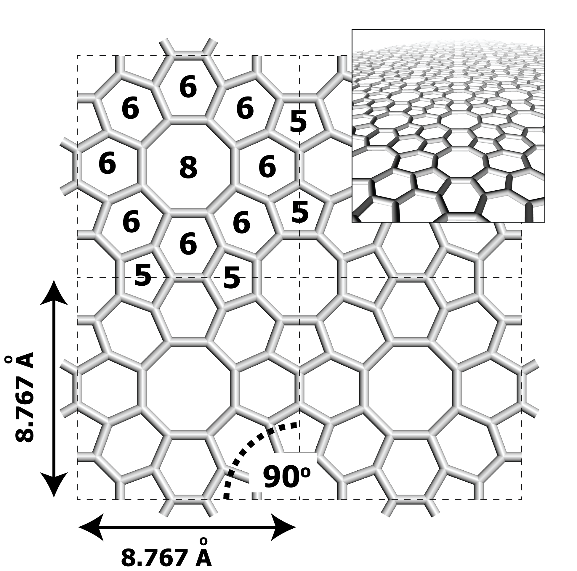
The new allotrope has a primitive cell with 28 atoms composed in pentagons, hexagons, and octagons. It has a planar density of 0.364 atoms per , comparable to 0.380 atoms per for graphene. The central geometrical feature is an octagon completely surrounded by hexagons. The cell geometry is square with p4/MMM symmetry. A Hessian linear vibrational analysis showed the structure to be a local energy minimum. Room temperature quantum molecular dynamics simulations were also used to confirm its stability.
As a final check on the ground state structure, the cell geometry and linear stability were verified using a second DFT implementation that employs a plane-wave basis set VASP3 ; VASP4 . A Projector Augmented Wave approach VASPpaw1 was used within a Generalized Gradient Approximation VASP-GGA1 . The wave function energy cutoff was set at 400 eV, and a conjugate gradient method employing a 4x4x2 Monkhorst-Pack grid resulted in the same ground state structure but with a lattice constant of 8.674 Å.
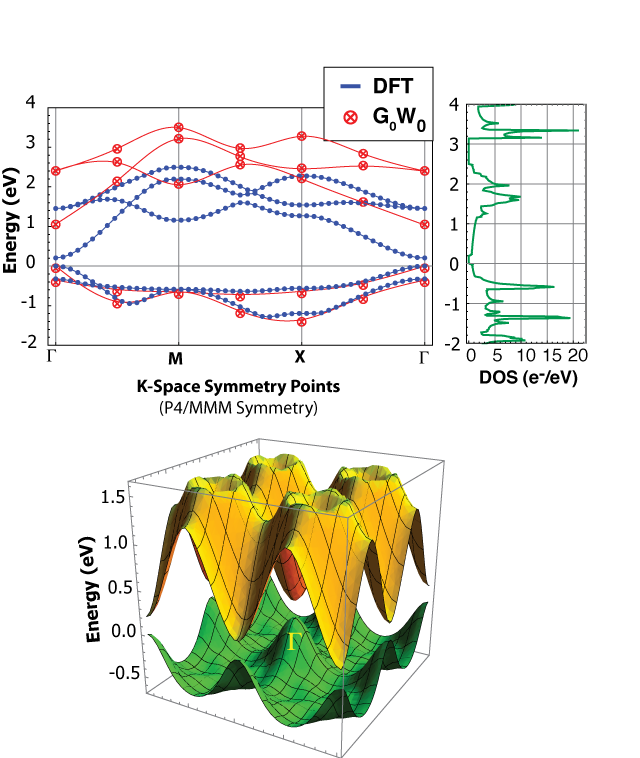
The plane-wave DFT code was subsequently used to predict both the band structure (BS) and Density of States (DOS). A 24x24x1, -centered k-space grid was used to calculate the electronic properties. The BS and DOS diagrams are shown in Figure 3. The material possesses a 0.2 eV direct band gap at the point. As in graphene, all carbon atoms bond with three nearest neighbors, but the symmetry of the in-plane sp-2 character has been disrupted by the varying bond angles and bond lengths.
DFT typically underestimates the band gap of periodic structures ref:payne-iterative-minimization , so the 0.2 eV gap should be viewed as a lower bound. Many-body perturbation theory, within the approximation Shishkin2007 , was therefore used to provide a more accurate estimate of the electronic structure. As expected, the inclusion of quasi-particle effects widens the band gap, providing an estimate for the direct, point gap of 1.1 eV. The band structure is shown with its DFT counterpart in Figure 3. Three iterations towards self-consistency ( approximation) opened the band gap slightly to 1.2 eV.
Having elucidated the lattice and electronic structure of this new material, we now examine its defect architecture. Such decompositions are not intended as prescriptive synthesis steps and are, rather, a way of understanding the properties of graphene allotropes from the broader perspective of defects from which they are composed. All Haeckelite allotropes can be constructed from graphene with templates of either STW defects or a combination of STW and ISTW defects ref:LuskCarr2009 . Likewise dimerites, as the name suggests, amount to graphene on which a regular grid of ISTW defects have been applied ref:LuskCarr2009 . The new semiconducting allotrope, however, requires the addition of di-vacancies (DV) to the defect alphabet. By patterned placement of DVs and STW defects, Octite SC can be engineered from graphene.
We schematically illustrate the defect composition in Figure 4. Initially a DV defect is introduced as shown in Figure 4(a). Two bond rotation defects are subsequently imposed (frames b and c). The result is then replicated so as to create an array of octagonal defects. Octagons surrounded by hexagons result from DV and STW defects while smaller octagons surrounded by alternating pentagons and hexagons derive from STW defects (frame d).
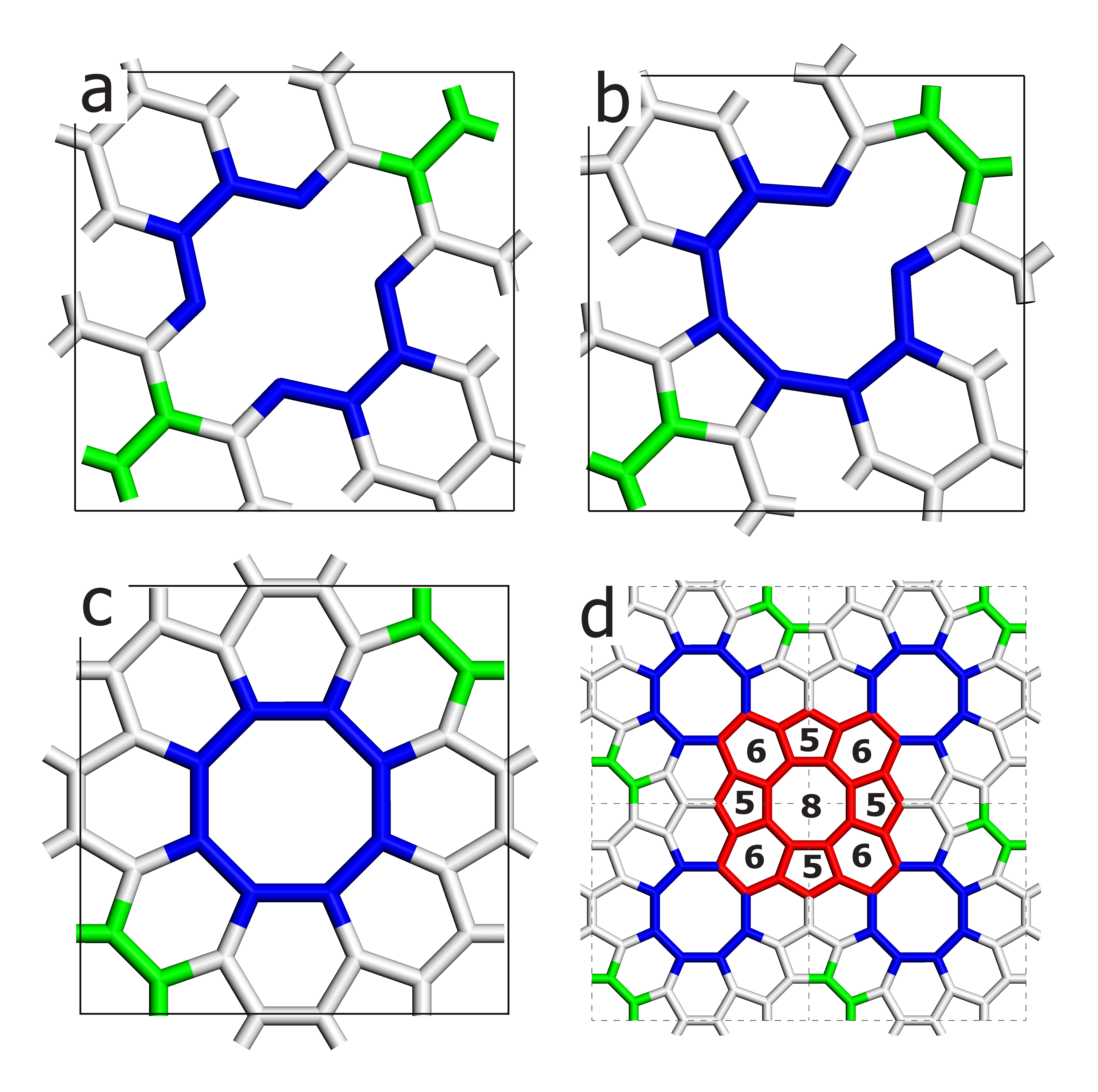
The formation energy associated with each defect shown in Figure 4 was calculated within a periodic 200 atom supercell as well as on a passivated, 206-atom flexible graphene flake. The formation energy of the DV was found to be 7.6 eV in the periodic supercell, in good agreement with previous periodic DFT estimates of 7.5 eV ref:Kotakoski2006 and 8.7 eV ref:ElBarbary2003 . The flexible boundaries of the graphene flake allowed the formation energy to be substantially lower at 6.6 eV. We calculate that the subsequent bond rotation defects on the right and left of the DV result in sequential, net increases of 4.7 eV and 5.1 eV for the periodic supercell or 5.0 eV and 5.1 eV for the graphene flake.
DV defects, central to the structure of Octite SC, can be precisely created via irradiation ref:Hashimoto2004 . Recently, an electron irradiation beam focused to was shown to be capable of precisely creating vacancies in CNTs ref:Banhart2009 . The stability of DVs has also been considered theoretically within a CNT setting, where molecular dynamics annealing predicted that they will remain stable in the 5-8-5 configuration up to at least 2700 K ref:Yuan2009 and 3000 K ref:Sammalkorpi2004 . Tight-binding molecular dynamics studies at higher temperatures concluded that DVs were stable out to 3100K for at least the 90 ps computational experiment ref:Lee2005 . A subsequent temperature increase to 3800 K was required to cause this 5-8-5 defect to relax to the slightly lower energy 555-777 defect with an estimated barrier of 5.2 eV ref:Lee2005 . Our own transition state analysis estimated a similar barrier of 3.7 eV for relaxation from a 6-8-6 defect to a 555-777 defect. These results suggest that the DV defect, central to Octite SC, should be stable for the operating conditions expected of standard electronic circuitry.
STW defects have been extensively studied in both graphene ref:Li2005 ; ref:stone1986 and CNTs ref:Kotakoski2006 ; ref:Kim2006 . STW defects could be created or reversed by scanning tunneling microscopy (STM) ref:berthe2007 or atomic force microscopy (AFM) ref:sugimoto2005 . Both DV and STW defects have been experimentally observed ref:Banhart2009 ; ref:Hashimoto2004 ; ref:Urita2005 .
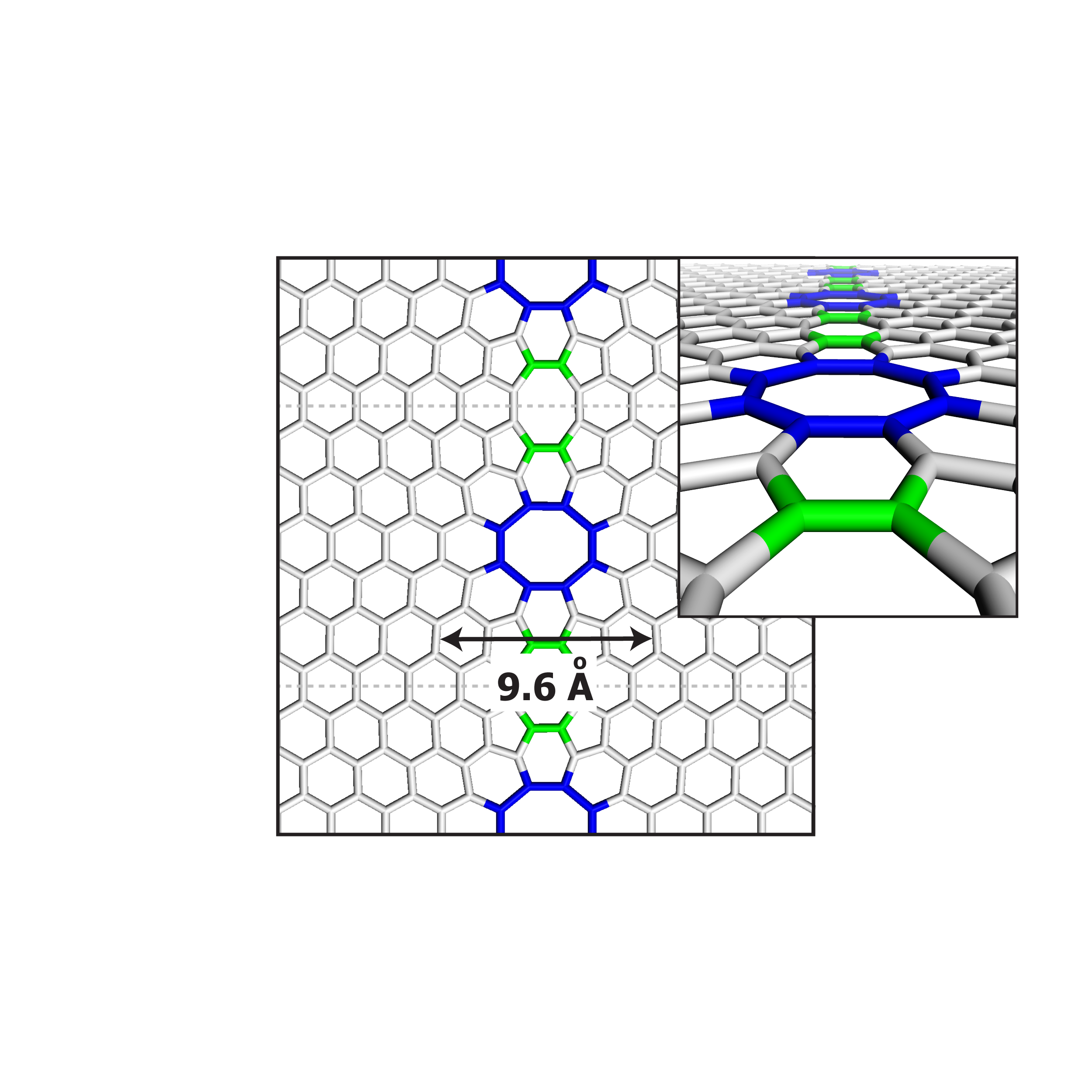
Semiconducting ribbons can be built into graphene as shown in Figure 5. Our DFT calculations predict that these ribbons remain planar within the graphene, and preliminary results suggest that the semiconducting character is locally preserved. Analogous conducting structures can also be designed, and our prediction of a metallic defect ribbon has already been experimentally verified ref:Batzill2010 ; ref:AppelhansThesis . Semiconducting and conducting ribbons, embedded within graphene, could be used together as the basis for electronic logic circuits.
In summary, we have found that patterned defects involving DVs yield a planar, single-atomic layer material composed entirely of carbon that is an intrinsic semiconductor; no external agencies or special boundary conditions need to be imposed in order to open up a band gap. In comparison with epitaxial paradigms, this is particularly attractive since suspended graphene possesses a mobility ten times that of graphene fabricated on a substrate ref:Bolotin2008 . Future electronics designs can exploit local and extended defects to build free standing, single-atomic layer logic circuits based on the local symmetry properties of carbon bonds.
I Acknowledgements
We are pleased to acknowledge the use of computing resources provided through the Golden Energy Computing Organization (NSF Grant No. CNS-0722415) and the Renewable Energy MRSEC program (NSF Grant No. DMR-0820518) at the Colorado School of Mines.
References
- (1) K. S. Novoselov, Nat. Mater. 6, 720 (2007).
- (2) A. K. Geim and K. S. Novoselov, Nat. Mater. 6, 183 (2007).
- (3) K. Bolotin, K. Sikes, Z. Jiang, M. Klima, G. Fudenberg, J. Hone, P. Kim, and H. Stormer, Solid State Commun. 146, 351 (2008).
- (4) Y.-M. Lin, C. Dimitrakopoulos, K. A. Jenkins, D. B. Farmer, H.-Y. Chiu, A. Grill, and P. Avouris, Science 327, 662 (2010).
- (5) F. Schedin, A. K. Geim, S. V. Morozov, E. W. Hill, P. Blake, M. I. Katsnelson, and K. S. Novoselov, Nat. Mater. 6, 652 (2007).
- (6) C. Lee, X. Wei, J. W. Kysar, and J. Hone, Science 321, 385 (2008).
- (7) K. S. Novoselov, A. K. Geim, S. V. Morozov, D. Jiang, M. I. Katsnelson, I. V. Grigorieva, S. V. Dubonos, and A. A. Firsov, Nature 438, 197 (2005).
- (8) T. Ohta, A. Bostwick, T. Seyller, K. Horn, and E. Rotenberg, Science 313, 951 (2006).
- (9) G. Giovannetti, P. A. Khomyakov, G. Brocks, P. J. Kelly, and J. van den Brink, Phys. Rev. B 76, 073103 (2007).
- (10) S.-Y. Kwon, C. V. Ciobanu, V. Petrova, V. B. Shenoy, J. Bareo, V. Gambin, I. Petrov, and S. Kodambaka, Nano Lett. 9, 3985 (2009).
- (11) Y. Zhang, J. P. Small, W. V. Pontius, and P. Kim, Appl. Phys. Lett. 86, 073104 (2005).
- (12) J. Nilsson, A. H. C. Neto, F. Guinea, and N. M. R. Peres, Phys. Rev. B 76, 165416 (2007).
- (13) L. Brey and H. A. Fertig, Phys. Rev. B 73, 235411 (2006).
- (14) E. R. Mucciolo, A. H. Castro Neto, and C. H. Lewenkopf, Phys. Rev. B 79, 075407 (2009).
- (15) O. Hod, V. Barone, J. E. Peralta, and G. E. Scuseria, Nano Lett. 7, 2295 2299 (2007).
- (16) V. Barone, O. Hod, and G. E. Scuseria, Nano Lett. 6, 2748 2754 (2006).
- (17) J. Bai, X. Zhong, S. Jiang, Y. Huang, and X. Duan, Nat. Nanotechnol. 5, 190 (2010).
- (18) J. O. Sofo, A. S. Chaudhari, and G. D. Barber, Phys. Rev. B 75, 153401 (2007).
- (19) D. A. Dikin, S. Stankovich, E. J. Zimney, R. D. Piner, G. H. B. Dommett, G. Evmenenko, S. T. Nguyen, and R. S. Ruoff, Nature 448, 457 (2007).
- (20) L. Ci, L. Song, C. Jin, D. Jariwala, D. Wu, Y. Li, A. Srivastava, Z. F. Wang, K. Storr, L. Balicas, F. Liu, and P. M. Ajayan, Nat. Mater. 9, 430 (2010).
- (21) V. H. Crespi, L. X. Benedict, M. L. Cohen, and S. G. Louie, Phys. Rev. B 53, R13303 (1996).
- (22) H. Terrones, M. Terrones, E. Hern ndez, N. Grobert, J. C. Charlier, and P. M. Ajayan, Phys. Rev. Lett. 84, 1716 (2000).
- (23) M. T. Lusk and L. Carr, Carbon 47, 2226 (2009).
- (24) D. Appelhans, Ph.D. thesis, Colorado School of Mines, 2009.
- (25) A. Stone and D. J. Wales, Chem. Phys. Lett. 128, 501 (1986).
- (26) P. A. Thrower and R. M. Mayer, Phys. Status Sol. A 47, 11 (1978).
- (27) M. T. Lusk and L. D. Carr, Phys. Rev. Lett. 100, 175503 (2008).
- (28) M. T. Lusk, D. T. Wu, and L. D. Carr, Phys. Rev. B 81, 155444 (2010).
- (29) J. da Silva-Araújo, H. Chacham, and R.W. Nunes, Phys. Rev. B 81, 193405 (2010).
- (30) B. Delley, Journal of Chemical Physics 92, 508 (1990).
- (31) J. P. Perdew and Y. Wang, Phys. Rev. B 45, 13244 (1992).
- (32) G. Kresse and J. Furthmuller, Comp. Mater. Sci. 6, 15 (1996).
- (33) G. Kresse and J. Furthmuller, Phys. Rev. B 54, 11169 (1996).
- (34) P. E. Blöchl, Phys. Rev. B 50, 17953 (1994).
- (35) J. P. Perdew, J. A. Chevary, S. H. Vosko, K. A. Jackson, M. R. Pederson, D. J. Singh, and C. Fiolhais, Phys. Rev. B 46, 6671 (1992).
- (36) M. C. Payne, M. P. Teter, D. C. Allan, T. A. Arias, and J. D. Joannopoulos, Rev. Mod. Phys. 64, 1045 (1992).
- (37) M. Shishkin and G. Kresse, Phys. Rev. B 75, 235102 (2007).
- (38) J. Kotakoski, A. V. Krasheninnikov, and K. Nordlund, Phys. Rev. B 74, 245420 (2006).
- (39) A. A. El-Barbary, R. H. Telling, C. P. Ewels, M. I. Heggie, and P. R. Briddon, Phys. Rev. B 68, 144107 (2003).
- (40) A. Hashimoto, K. Suenaga, A. Gloter, K. Urita, and S. Iijima, Nature 430, 870 (2004).
- (41) J. A. Rodriguez-Manzo and F. Banhart, Nano Lett. 9, 2285 2289 (2009).
- (42) J. Yuan and K. Liew, Carbon 47, 1526 (2009).
- (43) M. Sammalkorpi, A. Krasheninnikov, A. Kuronen, K. Nordlund, and K. Kaski, Phys. Rev. B 70, 245416 (2004).
- (44) G.-D. Lee, C. Z. Wang, E. Yoon, N.-M. Hwang, D.-Y. Kim, and K. M. Ho, Phys. Rev. Lett. 95, 205501 (2005).
- (45) L. Li, S. Reich, and J. Robertson, Phys. Rev. B 72, 184109 (2005).
- (46) G. Kim, B. W. Jeong, and J. Ihm, Appl. Phys. Lett. 88, 193107 (2006).
- (47) M. Berthe, S. Yoshida, Y. Ebine, K. Kanazawa, A. Okada, A. Taninaka, O. Takeuchi, N. Fukui, H. Shinohara, S. Suzuki, K. Sumitomo, Y. Kobayashi, B. Grandidier, D. Stievenard, and H. Shigekawa, Nano Lett. 7, 3623 (2007).
- (48) Y. Sugimoto, M. Abe, S. Hirayama, N. Oyabu, O. Custance, and S. Morita, Nature Mater. 4, 156 (2005).
- (49) K. Urita, K. Suenaga, T. Sugai, H. Shinohara, and S. Iijima, Phys. Rev. Lett. 94, 155502 (2005).
- (50) J. AU Lahiri, Y. Lin, P. Bozkurt, I. I. Oleynik, and M. Batzill, Nat. Nanotechnol. 5, 326 (2010).