Corresponding author: S. Burger
URL: http://www.zib.de/Numerik/NanoOptics/
URL: http://www.jcmwave.com
Email: burger@zib.de
Numerical Investigation of Photonic Crystal Microcavities in Silicon-on-Insulator Waveguides
Abstract
Optical resonances in 1D photonic crystal microcavities are investigated numerically using finite-element light scattering and eigenmode solvers. The results are validated by comparison to experimental and theoretical findings from the literature. The influence of nanometer-scale geometry variations on the resonator performance is studied. Limiting factors to ultra-high Q-factor performance are identified.
keywords:
optical microcavity, nanooptics, integrated optics, 3D Maxwell solver, finite-element methodThis paper will be published in Proc. SPIE Vol. 7609 (2010) 76091Q, (Photonic and Phononic Crystal Materials and Devices X, Ali Adibi, Shawn-Yu Lin, Axel Scherer, Editors) and is made available as an electronic preprint with permission of SPIE. Copyright 2010 Society of Photo-Optical Instrumentation Engineers. One print or electronic copy may be made for personal use only. Systematic reproduction and distribution, duplication of any material in this paper for a fee or for commercial purposes, or modification of the content of the paper are prohibited.
1 Introduction
Integration of optical components with electronic circuits promises to provide increased functionality. Building blocks of such integrated optical devices are waveguides, modulators, switches, and others. Due to their high quality factor (Q-factor) and small modal volume, one dimensional photonic crystal (PhC) microcavities in silicon-on-insulator are candidates for integrated all-optical switching devices. High Q-factors have been reported for such devices by Zain et al [1]. Further realized designs of optical microcavities include 2D photonic crystal resonators [2], suspended air-bridge cavities [3] and circular grating resonators [4].
In this contribution we numerically investigate high-Q resonances in PhC microcavities, where we partially review results of an earlier contribution [5]. We analyse the photonic devices through numerical simulations of light propagation using a time-harmonic finite-element method (FEM) light scattering solver. The method is validated by comparison to experimental and theoretical results, and the effect of small geometry variations on device performance is investigated. We further use an eigenmode solver for direct computation of resonance wavelengths and Q-factors. The light scattering solver, the eigenmode solver as well as a propagation mode solver used for computing incident waveguide modes are parts of the commercial FEM programme package JCMsuite, which is developed by JCMwave and ZIB [6]. The solvers enable fast and accurate simulations of main properties of optical microcavities.
2 Investigated Setup
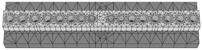
The investigated setup consists of a silicon waveguide with square shape which is perforated with a number of cylindrical air pores (PhC) and is supported by a silica substrate. The cavity essentially is formed by a missing central pore. Diameters and positions of the air pores are fine-tuned for high quality and transmission [7]. For the FEM simulations we discretize this geometry by prismatoidal elements. Figure 1 shows a part of the spatial mesh. A typical computational domain has a size of corresponding to roughly cubic wavelengths (in Si). The model extends waveguide, substrate and surrounding air to infinity by applying transparent boundary conditions to the corresponding faces. The material relative permittivities are (Si) and (SiO2), the waveguide width and height are nm and nm. Air holes with diameters nm, nm, nm, nm, nm (holes with repeat times), are positioned symmetrically around the cavity center with center to cavity-center distances : (where is the cavity length, nm), nm, nm, nm, nm, nm. This setup has been investigated experimentally and theoretically by Velha et al for nm [7]. We have extended the investigation to a fine sampling of cavity lengths on a nanometer scale, and we investigate pore sidewall angles different from 90 degrees.
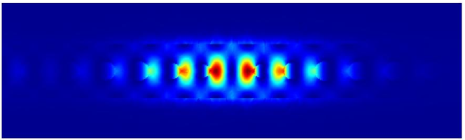
For simulating transmission through the microcavity at specific wavelength , we first compute the fundamental propagation mode of the waveguide at using a FEM propagating mode solver [8]. The obtained mode field is applied as input data to one of the boundaries of the 3D computational domain (left boundary in Fig. 1), such that the mode propagates in direction of the center of the waveguide. We then compute the scattered light field in the setup corresponding to this excitation using higher-order finite-elements. In post-processes we extract energy fluxes through interfaces and field distributions in several cross-sections from the 3D light field distribution. Figure 2 visualizes the computed electric field intensity at an incident wavelength close to the cavity’s resonance wavelength.
3 Numerical Results
3.1 Validation of FEM results
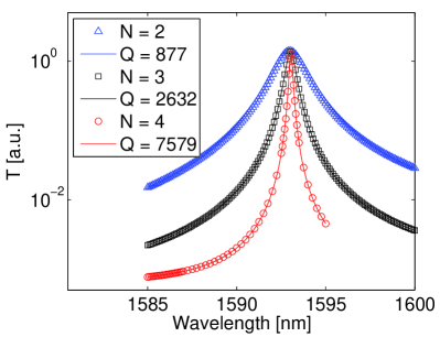
In order to compare results obtained with our method to results obtained with a dedicated Fourier modal method (RCWA) [9, 7] and to experimental results [7] we have performed wavelength scans over cavity resonances for cavity lengths nm [5]. Figure 3 shows the corresponding transmission spectra for cavities with a total number of 12/14/16 PhC holes, resp. for . As expected, for all three cases we find clear resonances in the transmission spectra. All resonances are centered around a peak wavelength of about nm. From the ratio of to the widths of Lorentz fits to the distributions we find Q-factors of for . The simulated peak wavelengths correspond very well to experimental results of Velha et al (nm for ) and to numerical results of Velha et al (nm). The Q-factors obtained with our method are slightly below the experimental and numerical values from Velha et al (, ).
To further validate our results we have performed a convergence analysis showing that with moderate computational effort in the range of minutes of computation time for a single frequency we reach accuracies of the resonance wavelength of better than 0.1%, and of high Q-factors [1] in the few percent range.
3.2 Investigation of geometry variations on a nanometer-scale
We have performed numerical experiments with slight variations of some geometrical parameters [5]. This allows to quantify the influence of fabrication tolerances on microcavity properties. Due to spatial adaptivity of the used unstructured meshes, FEM allows to investigate influences of very small variations of the geometry at high accuracy and without additional computational costs.
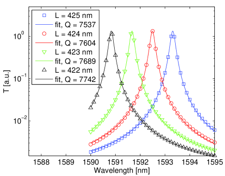
In a first set of simulations we have performed wavelength scans for PhC cavities with 12 air pores () for cavity lengths of nm. Figure 4 (left) shows the corresponding transmission spectra. As can be seen from these spectra and from the fitted distributions, in the investigated regime, a shift of shifts the resonance wavelength approximately linearly with . Also, a decrease of by about one percent increases by about 4% in the investigated regime. This shows that fabrication tolerances in the range of few nanometers can well explain significant deviations of device performance. The slight shift of resonance wavelength with respect to the data displayed in Fig. 3 of about 0.02% is due the lower numerical resolution of the simulations displayed in Fig. 4 (left).
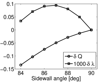
In a second set of experiments we have varied the sidewall angle (SWA) of all air pores between 84 and 90 degrees (90 deg. corresponds to perpendicular SWA, resp. cylindrical shape). For a better comparability of the results, for SWA 90 degrees the upper radius of the air pore was increased, the lower radius was decreased, and the radius at central waveguide height was kept constant. Figure 4 (right) shows corresponding results: While the influence of pore SWA on resonance wavelength can be neglected in the investigated regime, the influence of pore SWA on Q-factor is significant: A deviation of 5 degrees from vertical sidewalls decreases the Q-factor by about 10 percent.
3.3 Direct simulation of cavity resonances
Alternatively to simulating the light scattering response of the device, we can also use an eigenmode solver for directly simulating the resonance properties (resonance wavelength and Q-factor): Given the geometrical setup as described in Section 2, one computes an electric field distribution and a complex eigenfrequency which satisfy Maxwell’s time-harmonic wave equation
without sources; electric permittivity and magnetic permeability are denoted by and , respectively. Transparent boundary conditions take into account the specific geometry of the problem where waveguides are modelled to extend to infinity in the exterior domain [10]. When the eigenmode () is computed, the respective -factor is deduced from the real and imaginary parts of the complex eigenfrequency, the resonance wavelength is given by , with the speed of light .
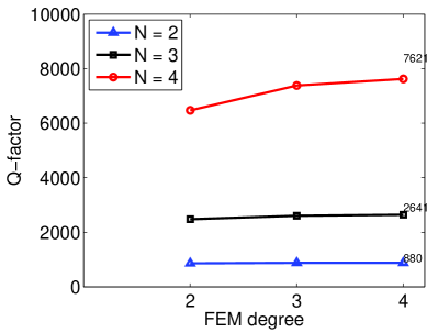
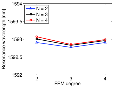
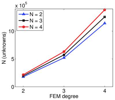
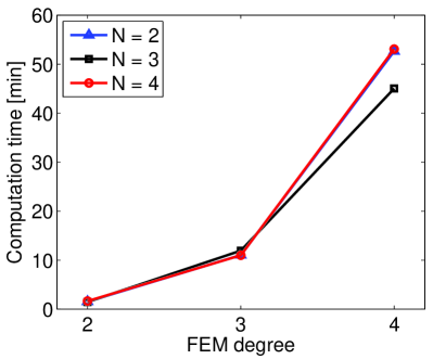
Figure 5 shows the convergence of the computed -factors and resonance wavelengths for the cases investigated also in Section 3.1 (). Here we have increased the numerical resolution by increasing the polynomial degree of the chosen finite element ansatz-functions. As can be seen from this figure, both, Q-factor and resonance wavelength computed with the eigenmode solver converge to the values obtained from the light scattering simulations (c.f. Section 3.1). Figure 6 shows the computational costs corresponding to these simulations. Please note that simulating a resonance directly requires a single computation only while deducing the resonance properties from a transmission or reflection simulation (as in Section 3.1) always requires several computations at various wavelengths. Especially for high-Q resonances, where the choice of such wavelengths for a transmission scan is not clear a-priori, direct computation of resonances greatly simplifies the simulation task and reduces computational effort.
3.4 Simulation of high-Q resonators
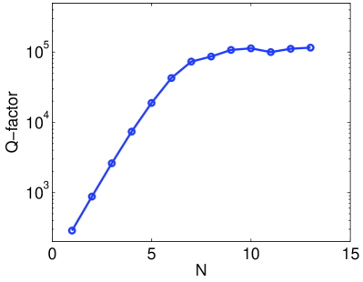
In a 3D photonic crystal setup one expects that the cavity Q-factor will increase exponentially with the width of the surrounding photonic crystal when a cavity is operated inside a bandgap. However, in the given 1D photonic crystal setup, the situation is different because leakage to the substrate and to surrounding air regions also have to be taken into account. In a further set of numerical experiments we have applied the eigenmode FEM solver in order to adress the question which Q-factors can be reached by simply adding more and more pores to the 1D PhC microcavity. Figure 7 (left) shows that the cavity Q-factor increases exponentially with the size of the photonic crystal region for numbers of pores in the periodic sections of the design, , between 1 and about 6. For higher , a plateau of is reached.
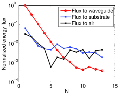
By integrating over the flux of energy density over the computational domain boundaries in the different material regions we have further recorded the losses to the substrate, to the surrounding air region, and to the waveguide region. Figure 7 (right) shows the corresponding results. In accordance with Fig. 7 (left), for below , the losses to substrate and surrounding air region do not play a significant role (note the logarithmic scale of the plot). As in this regime the resonator looses its energy mainly through the waveguide, the photonic crystal perforation of the waveguide yields an exponential decay of the field and exponentially lower losses with increasing the width of the waveguide. For light scattering to the substrate and to the surrounding air regions are the dominant loss channels, and further improvement of the photonic crystal in the waveguide region does therefore not lead to an improvement of the quality factor beyond the values reached at .
4 Conclusion
Finite-element solvers have been used to numerically investigate photonic crystal microcavities. The results have been validated by comparison to experimental and theoretical results from the literature. Further, numerical solutions from a scattering solver and numerical solutions from an eigenmode solver have been shown to yield an excellent agreement of physical results within the limits of numerical errors. The influence of nanometer-scale geometry variations (placement and sidewall angle) on the performance of one-dimensional PhC microcavities has been investigated. Losses to substrate and air regions have been identified as limiting factors to ultra-high Q-factor performance of the investigated specific photonic crystal microcavity design.
Acknowledgments
We acknowledge support by the German Federal Ministry of Education and Research, BMBF, under contract No. 13N9071.
References
- [1] Zain, A. R. M., Johnson, N. P., Sorel, M., and De La Rue, R. M., “Ultra high quality factor one dimensional photonic crystal/photonic wire micro-cavities in silicon-on-insulator (SOI),” Opt. Express 16(16), 12084 (2008).
- [2] Tanaka, Y., Asano, T., and Noda, S., “Design of photonic crystal nanocavity with Q-factor of ,” J. Lightwave Technol. 26(11), 1532–1539 (2008).
- [3] Ripin, D. J., Lim, K.-Y., Petrich, G. S., Villeneuve, P. R., Fan, S., Thoen, E. R., Joannopoulos, J. D., Ippen, E. P., and Kolodziejski, L. A., “Photonic band gap airbridge microcavity resonances in GaAs/AlxOy waveguides,” Journal of Applied Physics 87(3), 1578–1580 (2000).
- [4] Schönenberger, S., Moll, N., Stöferle, T., Mahrt, R. F., Offrein, B. J., Götzinger, S., Sandoghdar, V., Bolten, J., Wahlbrink, T., Plötzing, T., Waldow, M., and Först, M., “Circular grating resonators as small mode-volume microcavities for switching,” Opt. Express 17(8), 5953 (2009).
- [5] Burger, S. and Zschiedrich, L., “Numerical investigation of silicon-on-insulator 1D photonic crystal microcavities,” in [Theoretical and computational nanooptics: Proceedings of the 2nd International Workshop ], Chigrin, D. N., ed., 1176, 43–45, AIP (2009).
- [6] Burger, S., Zschiedrich, L., Pomplun, J., and Schmidt, F., “JCMsuite: An adaptive FEM solver for precise simulations in nano-optics,” in [Integrated Photonics and Nanophotonics Research and Applications ], ITuE4, Optical Society of America (2008).
- [7] Velha, P., Rodier, J. C., Lalanne, P., Hugonin, J. P., Peyrade, D., Picard, E., Charvolin, T., and Hadji, E., “Ultra-high-reflectivity photonic-bandgap mirrors in a ridge SOI waveguide,” New Journal of Physics 8(9), 204 (2006).
- [8] Pomplun, J., Zschiedrich, L., Klose, R., Schmidt, F., and Burger, S., “Finite element simulation of radiation losses in photonic crystal fibers,” phys. stat. sol. (a) 204, 3822 (2007).
- [9] Cao, Q., Lalanne, P., and Hugonin, J.-P., “Stable and efficient Bloch-mode computational method for one-dimensional grating waveguides,” J. Opt. Soc. Am. A 19(2), 335 (2002).
- [10] Zschiedrich, L., Klose, R., Schädle, A., and Schmidt, F., “A new finite element realization of the Perfectly Matched Layer Method for Helmholtz scattering problems on polygonal domains in 2D,” J. Comput. Appl. Math. 188, 12–32 (2006).