Magnetotransport of Dirac Fermions on the surface of a topological insulator
Abstract
We study the properties of Dirac fermions on the surface of a topological insulator in the presence of crossed electric and magnetic fields. We provide an exact solution to this problem and demonstrate that, in contrast to their counterparts in graphene, these Dirac fermions allow relative tuning of the orbital and Zeeman effects of an applied magnetic field by a crossed electric field along the surface. We also elaborate and extend our earlier results on normal metal-magnetic film-normal metal (NMN) and normal metal-barrier-magnetic film (NBM) junctions of topological insulators [Phys. Rev. Lett. 104, 046403 (2010)]. For NMN junctions, we show that for Dirac fermions with Fermi velocity , the transport can be controlled using the exchange field of a ferromagnetic film over a region of width . The conductance of such a junction changes from oscillatory to a monotonically decreasing function of beyond a critical which leads to the possible realization of magnetic switches using these junctions. For NBM junctions with a potential barrier of width and potential , we find that beyond a critical , the criteria of conductance maxima changes from to for integer . Finally, we compute the subgap tunneling conductance of a normal metal-magnetic film-superconductor (NMS) junctions on the surface of a topological insulator and show that the position of the peaks of the zero-bias tunneling conductance can be tuned using the magnetization of the ferromagnetic film. We point out that these phenomena have no analogs in either conventional two-dimensional materials or Dirac electrons in graphene and suggest experiments to test our theory.
pacs:
71.10.Pm, 73.20.-rI Introduction
Topological insulators with time reversal symmetry in two and three dimensions (2D and 3D) have been studied extensively in recent years, both theoretically and experimentally zhang1 ; hasan1 ; kane1 ; kane2 ; qi1 ; exp2 ; expt1 ; hasan2 . The 3D topological insulators can be characterized by four integers and kane2 . The first integer specifies the class of topological insulators as strong () or weak (), while the last three integers characterize the time-reversal invariant momenta of the system given by , where are reciprocal lattice vectors. The topological features of strong topological insulators (STI) are robust against the presence of time-reversal invariant perturbations such as disorder and lattice imperfections. It has been theoretically predicted kane2 ; zhang1 and experimentally verified hasan1 that the surface of a STI has an odd number of Dirac cones whose positions are determined by the projection of on to the Brillouin zone of the surface. The position and number of these cones depend on both the nature of the surface concerned and the integers . For compounds such as and , specific surfaces with a single Dirac cone near the point of the 2D Brillouin zone have been found hasan1 ; exp2 ; hasan2 . Such a Dirac cone is described by the Hamiltonian
| (1) |
where denotes the Pauli (identity) matrices in spin space, is the annihilation operator for the Dirac spinor ( denotes the transpose of a row vector), is the Fermi velocity, and is the chemical potential kane4 . Recently, several novel features of these surface Dirac electrons such as the existence of Majorana fermions in the presence of a magnet-superconductor interface on the surface kane4 ; been1 , generation of time-reversal symmetric -wave superconducting state via proximity to a -wave superconductor kane4 , anomalous magnetoresistance of ferromagnet-ferromagnet junctions tanaka1 , and novel spin textures with chiral properties hasan2 have been studied in detail. Further it has been shown in Ref. mondal1, that it is possible to realize a magnetic switch by magnetically tuning the transport of Dirac fermions with a proximate ferromagnetic film. However, the response of these fermions in the presence of crossed electric and magnetic fields has not been studied so far. Another aspect of such fermions, namely, their transport through a normal metal-magnetic film-superconductor (NMS) junction has also not been explored.
In this work, we study several magnetotransport properties of these surface Dirac fermions in experimentally realizable situations. We first study the properties of the fermions in the presence of crossed magnetic [] and electric fields [] as shown in Fig. 1. We present an exact solution of this problem and show that for , the relative contributions of the Zeeman and the orbital terms to the Landau level energies, and hence their magnetic field dependence, can be tuned by varying either the strength of the applied electric field or the tilt of the applied magnetic field. We also show that for , the conductance of these Dirac fermions has an unconventional dependence on the tilt angle of the applied magnetic field and that this dependence can be used to realize electric-field controlled switching.
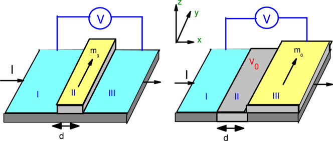
The second study involves an extension of the results obtained in Ref. mondal1, regarding transport in normal metal-magnetic film-normal metal (NMN) and normal metal-barrier-magnetic film (NBM) junctions of topological insulators. The relevant experimental geometries are shown in Fig. 2. We study the transport of these Dirac electrons across a region with a width where there is a proximity-induced exchange field arising from the magnetization of a proximate ferromagnetic film as shown in the left panel of Fig. 2. We demonstrate that the tunneling conductance of these Dirac fermions through such a junction can either be an oscillatory or a monotonically decaying function of the junction width . One can interpolate between these two qualitatively different behaviors of by changing (and thus ) by an applied in-plane magnetic field leading to the possible use of this junction as a magnetic switch. We also study the transport properties of Dirac fermions across a barrier characterized by a width and a potential in region II with a magnetic film proximate to region III as shown in the right panel of Fig. 2. We note that it is well known from the context of Dirac fermions in graphene neto1 that such a junction, in the absence of the induced magnetization, exhibits transmission resonances with maxima of transmission at , where is an integer. Here we show that beyond a critical strength of , the maxima of the transmission shifts to . Upon further increasing , one can reach a regime where the conductance across the junctions vanishes. We also point out that such NMN and NBM junctions can be used to determine the exact form of the Dirac Hamiltonian on the surface of the topological insulator.
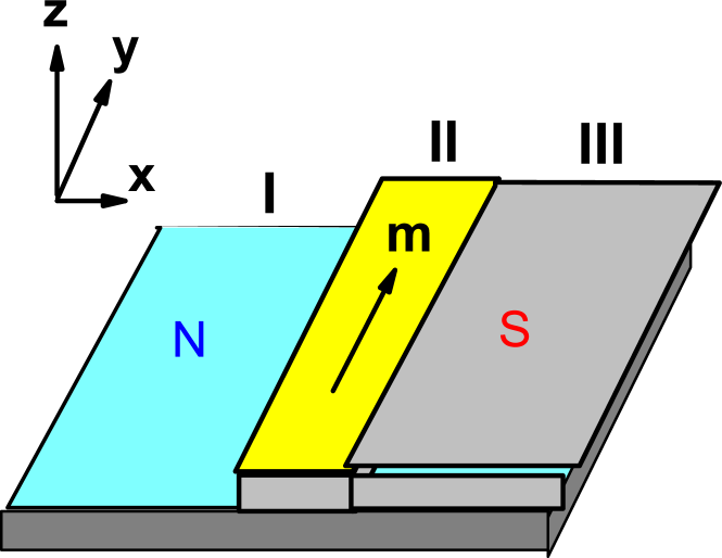
Finally, we study the transport of Dirac fermions across a NMS junction as shown in Fig. 3. The intermediate region (region II) in this junction has a thickness with a proximate ferromagnetic film providing a magnetization , while superconductivity is introduced in region III via the proximity effect. We provide a detailed analysis of the subgap tunneling conductance of these NMS junctions as a function of the applied voltage and magnetization . In particular, we point out that the positions of the maxima of the zero-bias tunneling conductance in such NMS junctions as a function of the width of the magnetic film can be varied by tuning the induced magnetization . We stress that the properties of the Dirac fermions elucidated in all these studies are a consequence of their spinor structure in physical spin space, and thus have no analogs for either conventional Schrödinger electrons in 2D or Dirac electrons in graphene kat1 ; comment1 ; comment2 .
The organization of the rest of the paper is as follows. In Sec. II, we study the properties of the Dirac fermions in the presence of crossed electric and magnetic fields. This is followed by the study of NMN and NBM junctions of these Dirac materials in Sec. III. In Sec. IV, we study the transport properties and subgap tunneling conductance of NMS junctions of topological insulators. Finally we discuss possible experimental verification of theory and conclude in Sec. V.
II Crossed electric and magnetic fields
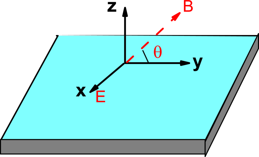
We begin with the properties of Dirac electrons in a crossed electric and magnetic field as shown in Fig. 1. The Hamiltonian for the Dirac Fermions for this case can be written as
where is the canonical momentum, is set to unity, is the gyromagnetic ratio, is the Bohr magneton, and we choose the vector potential to be . Note that here the Zeeman term does not determine the spin quantization axis of the Dirac electrons due to the presence of the term. Thus the in-plane component of the magnetic field, which enters the Hamiltonian only through the Zeeman term, only provides a constant shift to which can be gauged away. This property of the Dirac fermions is distinct from their counterpart in graphene. For , Eq. (LABEL:emham1) admits a straightforward solution and yields the Landau level spectrum
| (3) | |||||
where , is the magnetic length and we also define for later use. The state is non-degenerate as is also known from analogous studies of Landau levels in graphene neto1 . For the Dirac electrons on the surface of , m/s, so that leading to a negligible contribution of the Zeeman term in the spectrum.
The situation changes when an electric field is applied along . In this case, for , one can define a boost parameter and carry out a Lorentz transformation vinu1
| (4) |
where . In the boosted frame the Schrödinger equation reads
| (5) | |||||
Note that such a boost transformation affects the orbital part of the magnetic field only; the Zeeman field remains unchanged. The energy eigenvalues of Eq. (5) can be easily obtained and are given by
| (6) | |||||
where . Then a reverse boost to the “laboratory” frame yields
| (7) | |||||
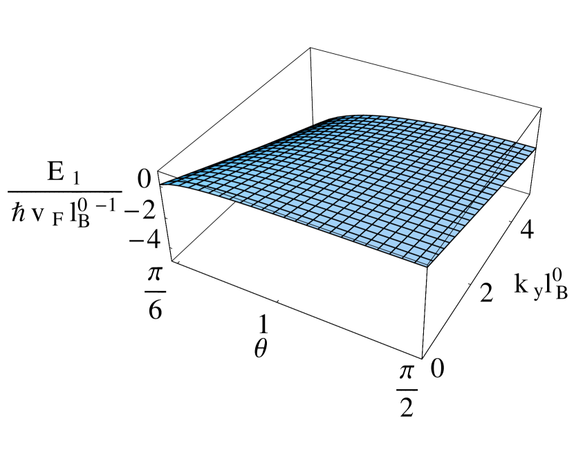
Eq. (7) is one of the central results of this section. It demonstrates that a collapse of the Landau levels for the Dirac fermions can be induced by varying either the electric field for a fixed tilt of the applied magnetic field or by varying the magnetic field tilt for a fixed electric field. A plot of the energy level as a function of this tilt and the transverse momentum is shown in Fig. 4.
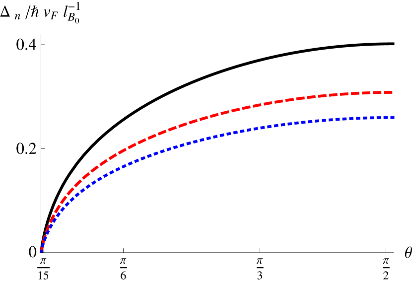
We also note that the magnetic field dependence of the Landau level energy gaps are different from their counter part in graphene. To illustrate this we define for . For , we find:
| (8) |
For when , we find that . This behavior is distinct from its counter part in graphene where for all . However, since /Tesla, this behavior can only be seen in a very tiny window near critical tilt and would be hard to figure out in experiments. On the contrary, the variation of dispersion of with the tilt angle , seen in Fig. 5 for several , can be tested experimentally with microwave absorption experiments routinely done for conventional quantum Hall systems qheexpt . This will be discussed further in Sec. V.
.
Now we turn to the solution of this problem in the regime where we get scattering states. In this regime, we define a parameter and perform a similar boost transformation as outlined earlier. This allows us to shift to a reference frame where there is no magnetic field and the Schrödinger equation, in the momentum representation, reads levitov1
| (9) | |||||
where and are the electric field and energy as seen in the boosted frame, and . The scattering states can now be easily obtained from this equation by noting the similarity of this equation with the standard Landau-Zenner problem with modified Planck’s constant . In particular, the transmission probability of these Dirac electrons in the direction of the applied electric field in the boosted frame can be written as
| (10) |
where is the legth scale set by the electric field. Now one can rotate back to the “laboratory frame” using , and integrate over modes to obtain the tunneling conductance levitov1
| (11) |
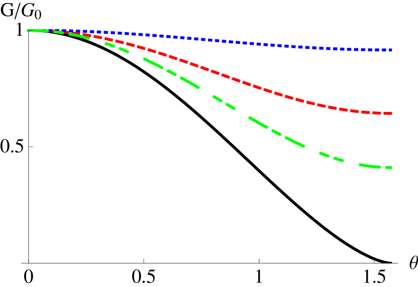
where , and is the sample width. We find that in contrast to graphene levitov1 , the Zeeman term arising from the magnetic field along produces an additional exponential suppression of the conductance. This can be understood by noting that in topological insulators, a Zeeman magnetic field along results in the generation of a mass term for the Dirac electrons and hence leads to a suppression of the conductance. A plot of as a function of the tilt of a magnetic field is shown in Fig. 6 for several representative values of the electric field and for a fixed magnetic field . The plot shows that for small electric fields, the conductance is quickly suppressed as we increase from to ; however for larger fields, the suppression is minimal. Thus one can tune the conductance of these insulators either by tuning the electric field at a fixed or by tuning at a fixed electric field.
III Transport in NMN and NBM junctions
In this section, we analyze the properties of NMN and NBM junctions of topological insulators as shown in the left and right panels of Fig. 2. Sec. III.1 discusses the NMN junctions while Sec. III.2 elucidates the properties of the NBM junctions.
III.1 NMN junctions
The proposed experimental set up for the NMN junction is shown in the left panel of Fig. 2. The Dirac fermions in region I and III are described by the Hamiltonian in Eq. (1). Consequently, the wave functions of these fermions moving along in these regions for a fixed transverse momentum and energy can be written as
| (12) |
where takes values I and III, and
| (13) |
In region II, the presence of the ferromagnetic strip with a magnetization leads to the additional term
| (14) |
where is the exchange field due to the presence of the strip tanaka1 , and denotes the Heaviside step function. Note that may be thought as a vector potential term arising due to a fictitious magnetic field . This analogy shows that our choice of the in-pane magnetization along is completely general; all gauge invariant quantities such as the transmission probability are independent of the -component of in the present geometry. We emphasize that this effect is distinct from that due to a finite component of which provides a mass to the Dirac electrons. For a given , the precise magnitude of depends on the exchange coupling of the film and can be tuned, for soft ferromagnetic films, by an applied field tanaka1 . The wave function for the Dirac fermions in region II moving along in the presence of such an exchange field is given by
| (15) |
where
| (16) |
Note that beyond a critical , and hence a critical , becomes imaginary for all leading to spatially decaying modes in region II.
Let us now consider an electron incident on region II from the left with a transverse momentum and energy . Taking into account reflection and transmission processes at and , the wave function of the electron can be written as
Here and are the reflection and transmission amplitudes, and () denotes the amplitude of right (left) moving electrons in region II. Matching boundary conditions on and at and and at leads to
| (18) |
Solving for from Eq. (18), one finally obtains the conductance
| (19) |
Here , is the density of states (DOS) of the Dirac fermions and is a constant for , is the sample width, and the transmission is given by
| (20) | |||||
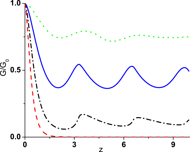
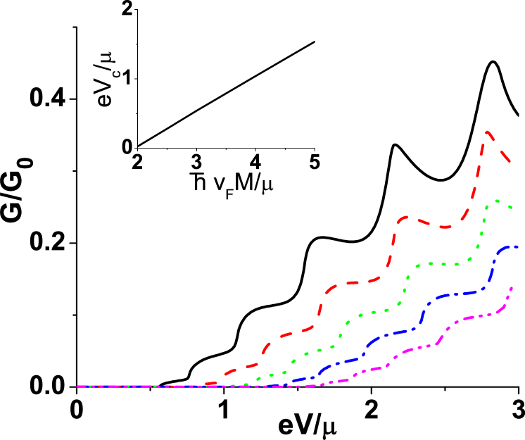
Eq. (20) and the expression for represent one of the main results of this section. We note that for a given , has an oscillatory (monotonically decaying) dependence on provided is real (imaginary). Since depends, for a given , on , we find that one can switch from an oscillatory to a monotonically decaying dependence of transmission in a given channel (labeled by or equivalently, ) by turning on a magnetic field which controls and hence . Also, since , we find that beyond a critical , the transmission in all the channels exhibits a monotonically decaying dependence on . Consequently, for a thick enough junction one can tune at fixed and from a finite value to nearly zero by tuning (i.e., ) through . Thus such a junction may be used as a magnetic switch. These qualitatively different behaviors of the junction conductance for below and above is demonstrated in Fig. 7 by plotting as a function of the effective barrier width for several representative values of . Since and hence depends on through the dimensionless parameter , this effect can also be observed by varying the applied voltage for a fixed , , and . In that case, for a reasonably large dimensionless barrier thickness , becomes finite only beyond a critical voltage as shown in Fig. 8 for several representative values of . The critical voltage can be determined numerically by finding the lowest voltage for which exhibits a monotonic decay as a function of . The plot of as a function of , shown in the inset of Fig. 8, demonstrates the expected linear relationship between and . We note that such a dependence of on or requires the Dirac electrons to be spinors in physical spin space, and is therefore impossible to achieve in either graphene neto1 or in a conventional 2D electron gas for which a proximate ferromagnetic film would only provide a Zeeman term for the electrons, leaving unaffected.
III.2 NBM junctions
Next, we analyze the NBM junction shown in the right panel of Fig. 2 where the region III below a ferromagnetic film is separated from region I by a potential barrier in region II. Such a barrier can be applied by changing the chemical region in region II either by a gate voltage or via doping exp2 . We will analyze the problem in the thin barrier limit in which and , keeping the dimensionless barrier strength finite. The wave function of the Dirac fermions moving along with a fixed momentum and energy in this region is given by
| (21) |
where
| (22) |
The wave functions in region I and III are given by and , where and are given in Eq. (LABEL:wav6). Note that one can have a propagating solution in region III only if .
The transmission problem for such a junction can be solved by a procedure similar to the one outlined above for the magnetic strip problem. For an electron approaching the barrier region from the left, we write down the following forms of the wave function in the three regions I, II and III: , , and . As outlined earlier, one can then match boundary conditions at and , and obtain the transmission coefficient as
| (23) | |||||
Note that in the absence of the ferromagnetic film over region III, , and . The expression for , reproduced here for the special case of , is well known from analogous studies in the context of graphene, and it exhibits both the Klein paradox ( for ) and transmission resonances ( for ) kat1 . When , we find that the transmission for normal incidence () does become independent of the barrier strength, but its magnitude deviates from unity:
| (24) |
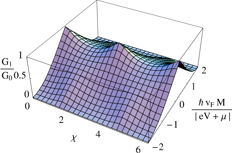
The value of decreases monotonically from for to for , and can thus be tuned by changing (or ) for a fixed (or ) and .
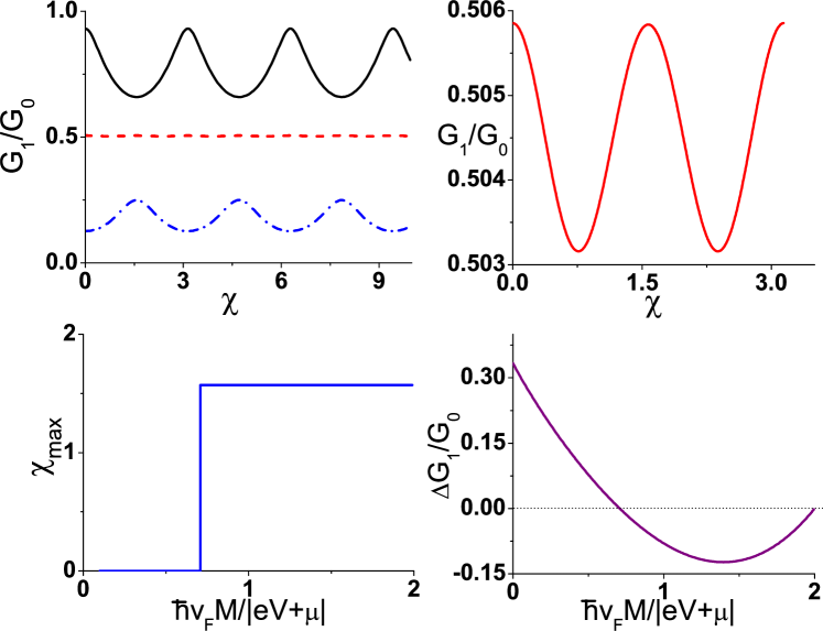
The conductance of this junction is given by , where are determined from the solution of for a given . A plot of as a function of and (for a fixed and ) is shown in Fig. 9. We find that the amplitude of decreases monotonically as a function of reaching at beyond which there are no propagating modes in region III. Also, as we increase , the conductance maxima shifts from to beyond a fixed value of as shown in the top left panel of Fig. 10. Numerically, we find . At , , leading to a period halving of from to . This is shown in the top right panel of Fig. 10 where is plotted as a function of . We note that near , the amplitude of oscillation of as a function of becomes very small so that is almost independent of . In the bottom left panel of Fig. 10, we plot (the value of at which the first conductance maxima occurs) as a function of which clearly demonstrates the shift. This is further highlighted by plotting as a function of in the bottom right panel of Fig. 10. crosses zero at indicating the position of the period halving. Thus the position of the conductance maxima depends crucially on and can be tuned by changing either or .
III.3 Alternative forms of the Hamiltonian
In this subsection, we discuss a possible way of distinguishing between possible forms of the Dirac Hamiltonian in the surface of a topological insulator. In the literature (see, for instance, Ref. xu, ), two such different forms have been studied for the first part of the Hamiltonian in Eq. (1), namely,
We have implicitly assumed the form in the entire analysis in this paper. We note that and are both time-reversal invariant since and under that transformation, and they are also invariant under rotations in the plane. But under the two-dimensional parity transformation and , they transform differently; since , , and , we see that while . Since the Hamiltonian of the surface Dirac electrons arises from a spin-orbit coupling in the bulk which is then projected on to the two-dimensional surface, and we have not discussed the bulk Hamiltonian here, we have no a priori reason to choose between and . In principal, we could even consider a linear combination of the two such as . Clearly, when an in-plane magnetization which breaks the in-plane rotational symmetry is introduced using the ferromagnetic film, the effect of this on the analysis in Secs. III.1 and III.2 will depend on the angle mentioned above; for instance, a magnetization in the direction will couple to and will therefore shift the momentum for and for . Hence, when experimental tests of the various results obtained in those two sections are performed, one can probe whether the Hamiltonian for the system of interest is actually or or a linear combination of the two, by varying the direction of magnetization of the ferromagnetic film and studying the effect that this has on the conductance. For example, if the hamiltonian describing the surface electrons of the topological insulator turns out to be , will have no effect on transport. In general, for any , there will be specific direction of the in-plane magnetization which will have maximal effect on the transport while the component of the magnetization will not affect the transport at all.
IV Transport in NMS junctions
We consider a NMS junction on the surface of a topological insulator as shown in Fig. 3. As shown there, region II, which extends from to , has a proximate ferromagnetic film leading to an induced magnetization . Region III depicts the superconducting region occupying . We assume that superconductivity in this regime is induced via a proximate superconducting film with -wave pairing as shown in the figure. The quasiparticles of such a superconductor can be described by the following Dirac-Bogoliubov-de Gennes equation kane2
| (26) |
where are the four components for the electron and the hole spinors, and the Hamiltonian is given by
| (27) |
where and are Heaviside step functions. is the BCS pair-potential in region III.
Eq. (1) can be solved for the normal, magnetic and superconducting regions. In the normal region, the wave functions for electron and hole moving in direction are given by
| (28) | |||||
| (29) | |||||
| (30) |
where the wave vector for the electron (hole) wave functions are given by
| (31) |
and is the angle of incidence of the electron (hole).
In region II, the wave functions for an electron and a hole moving in the direction are as follows:
| (32) | |||||
| (33) | |||||
| (34) |
where the wave vector of the electron (hole) wave function is given by
| (35) |
Here is the angle of incidence of the electron (hole). Note that in principle, we could have applied an additional gate voltage in this region as was done in Ref. kat1, . However, this leads to an expression of the longitudinal momentum
| (36) |
This shows that in the limit of large , the effect of on and hence on becomes negligible. Therefore we restrict ourselves to the limit.
In the superconducting region, the BdG quasiparticles are mixtures of electron and holes. Hence the wave function for BdG quasiparticles moving in directions with transverse momenta and energy for are given by
| (37) | |||||
| (38) |
and where denotes the Heaviside step function.
Next, we note that for any transmission process to take place we need . This condition gives the limits for the range of . For simplicity we consider in region II. Then . Using Eqs. (30), (34) and (38), we find that the Andreev process takes place for , where
| (39) | |||||
| (40) |
Note that , and this asymmetry is generated by the induced magnetization .
Following Ref. kat1, , we write wave functions for the normal, magnetic and superconducting regions as
| (41) | |||||
| (42) | |||||
| (43) |
where both normal and Andreev reflection are taken into account. Here and denote the amplitudes for normal and Andreev reflection respectively. These wave functions must satisfy the following boundary conditions,
| (44) |
Solving these boundary conditions, we obtain for and kat1
| (45) | |||||
| (46) | |||||
| (47) | |||||
| (48) | |||||
| (49) | |||||
| (50) |
where the parameters , and can be expressed as
| (51) | |||||
| (52) | |||||
| (53) |
The tunneling conductance of the NMS junction can be expressed in terms of and as
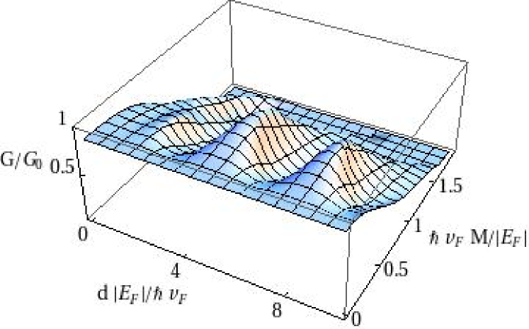
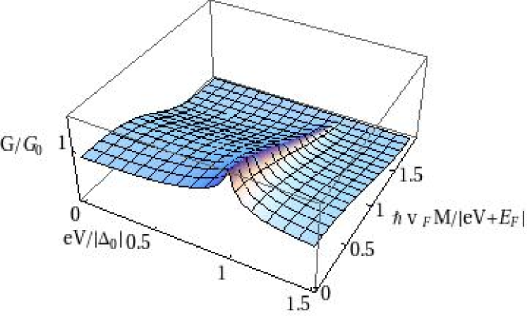
A plot of the subgap tunneling conductance as a function of the magnetization and the applied voltage for a fixed barrier width is shown in Fig. 11. We find that decreases monotonically as a function of the magnetization for all values of the applied voltage. This can be easily attributed to a decrease in the number of conduction channels (i.e., number of modes with real ) with increasing . The behavior of the zero-bias conductance as a function of the barrier width and magnetization is shown in Fig. 12. We find that the zero-bias conductance shows an oscillatory behavior as a function of the barrier width for small bhatt1 . With increasing , the position of the conductance maxima shifts which demonstrates the tunability of the zero-bias conductance with the induced magnetization. This continuous shift in position of the zero-bias conductance maxima is to be contrasted with the sudden change of its counterpart in NMN junctions of topological insulators.
V Experiments
Experimental verification of our work would involve carrying out the following experiments. For a topological insulator in a crossed electric and magnetic field with , we propose measurement of the energy gap of the Landau levels as a function of the electric field strength and the tilt angle . Such measurements have been done in quantum Hall systems using microwave absorption techniques qheexpt . The variation of the excitation energy gap between the ground and the first excited states, , as shown in Fig. 5, should be observable in similar experiments performed with topological insulators. For , we propose measurement of conductance of these films as a function of both the electric field and the tilt angle . We predict that for small , the tunneling should show a faster suppression with increase from to . We note that for a suitably chosen between and , the conductance of these films can tuned via an electric field, as demonstrated in Fig. 6, leading to realization of electric field controlled switching in these materials. For the NMN and NBM junctions, which can be prepared by depositing ferromagnetic films on the surface of a topological insulator, we propose measurement of the tunneling conductance as a function of . For the geometry shown in the left panel of Fig. 2, we predict that depending on the magnetization , should demonstrate either a monotonically decreasing or an oscillatory behavior as a function of the junction width . Another, probably more experimentally convenient, way to realize this effect would be to measure of a junction of width for several values of and confirm that varies linearly with with a slope of , provided and remain fixed. For the geometry depicted in the right panel of Fig. 2, one would, in addition, need to create a barrier by tuning the chemical potential of an intermediate thin region of the sample as done earlier for graphene neto1 . Here we also propose measurement of as a function of (or equivalently ) for several representative values of and a fixed . We predict that the maxima of the tunneling conductance would shift from to beyond a critical for a fixed , or equivalently, below a critical , for a fixed . Finally, for the NMS junction, we propose measurement of the tunneling conductance as a function of the magnetization which should demonstrate the decaying behavior shown in Fig. 11. The tunability of the zero-bias conductance maxima, shown in Fig. 12, can also be tested by making junctions with different widths.
In conclusion, we have studied several magnetotransport properties of Dirac Fermions on the surface of a topological insulator, and have shown that they exhibit several properties which are distinct both from their counterparts in graphene and conventional Schrodinger electrons in other 2D systems. These novel features include tunability of the orbital and Zeeman effects of an applied magnetic field with a crossed in-plane electric field, realization of a magnetic switch using a NMN junction, and magnetic tunability of transmission resonances of Dirac fermions in NBM and NMS junctions. We have suggested experiments which can verify our theory.
Acknowledgments
D.S. thanks DST, India for financial support under Project No. SR/S2/CMP-27/2006. K.S. thanks DST, India for financial support under Project No. SR/S2/CMP-001/2009 and K. Ray for several illuminating discussions on related topics.
References
- (1) B. A. Bernevig, T. L. Hughes, and S.-C. Zhang, Science 314, 1757 (2006); B. A. Bernevig and S.-C. Zhang, Phys. Rev. Lett. 96, 106802 (2006).
- (2) M. König, S. Wiedmann, C. Brüne, A. Roth, H. Buhmann, L. W. Molenkamp, X.-L. Qi, and S.-C. Zhang, Science 318, 766 (2007); D. Hsieh, D. Qian, L. Wray, Y. Xia, Y. S. Hor, R. J. Cava, and M. Z. Hasan, Nature 452, 970 (2008).
- (3) C. L. Kane and E. J. Mele, Phys. Rev. Lett. 95, 226801 (2005); ibid, Phys. Rev. Lett. 95, 146802 (2005).
- (4) L. Fu, C. L. Kane, and E. J. Mele, Phys. Rev. Lett. 98, 106803 (2007); R. Roy, Phys. Rev. B79, 195322 (2009); J. E. Moore and L. Balents, Phys. Rev. B75, 121306(R) (2007).
- (5) X. L. Qi, T. L. Hughes, and S. C. Zhang, Phys. Rev. B 78, 195424 (2008); H. Zhang, C.-X. Liu, X.-L. Qi, X. Dai, Z. Fang, and S.-C. Zhang, Nature Phys. 5, 438 (2009).
- (6) Y. Xia, D. Qian, D. Hsieh, L. Wray, A. Pal, H. Lin, A. Bansil, D. Grauer, Y. S. Hor, R. J. Cava, and M. Z. Hasan, Nature Phys. 5, 398 (2009); Y. Xia, D. Qian, D. Hsieh, R. Shankar, H. Lin, A. Bansil, A. V. Fedorov, D. Grauer, Y. S. Hor, R. J. Cava and M.Z. Hasan, arXiv:0907.3089 (unpublished).
- (7) Y. L. Chen, J. G. Analytis, J.-H. Chu, Z. K. Liu, S.-K. Mo, X. L. Qi, H. J. Zhang, D. H. Lu, X. Dai, Z. Fang, S. C. Zhang, I. R. Fisher, Z. Hussain, and Z.-X. Shen, Science 325, 178 (2009); T. Zhang, P. Cheng, X. Chen, J.-F. Jia, X. Ma, K. He, L. Wang, H. Zhang, X. Dai, Z. Fang, X. Xie, Q.-K. Xue, arXiv:0908.4136v3 (unpublished).
- (8) D. Hsieh, Y. Xia, D. Qian, L. Wray, J. H. Dil, F. Meier, J. Osterwalder, L. Patthey, J. G. Checkelsky, N. P. Ong, A. V. Fedorov, H. Lin, A. Bansil, D. Grauer, Y. S. Hor, R. J. Cava, and M. Z. Hasan, Nature 460, 1101 (2009); P. Roushan, J. Seo, C. V. Parker, Y. S. Hor, D. Hsieh, D. Qian, A. Richardella, M. Z. Hasan, R. J. Cava, and A. Yazdani, Nature 460, 1106 (2009); D. Hsieh, Y. Xia, L. Wray, D. Qian, A. Pal, J. H. Dil, J. Osterwalder, F. Meier, G. Bihlmayer, C. L. Kane, Y. S. Hor, R. J. Cava, and M. Z. Hasan, Science 323, 919 (2009).
- (9) L. Fu and C. L. Kane, Phys. Rev. Lett. 100, 096407 (2008).
- (10) A. R. Akhmerov, J. Nilsson, and C. W. J. Beenakker, Phys. Rev. Lett. 102, 216404 (2009); Y. Tanaka, T. Yokoyama, and N. Nagaosa, Phys. Rev. Lett. 103, 107002 (2009).
- (11) T. Yokoyama, Y. Tanaka, and N. Nagaosa, arXiv:0907.2810v2 (unpublished).
- (12) S. Mondal, D. Sen, K. Sengupta, and R. Shankar, Phys. Rev. Lett. 104, 046403 (2010).
- (13) A. H. Castro Neto, F. Guinea, N. M. R. Peres, K. S. Novoselov, and A. K. Geim, Rev. Mod. Phys. 81, 109 (2009); C. W. J. Beenakker, Rev. Mod. Phys. 80, 1337 (2008).
- (14) M. I. Katsnelson, K. S. Novoselov, and A. K. Geim, Nature Phys. 2, 620 (2006); C. W. J. Beenakker, Phys. Rev. Lett. 97, 067007 (2006); S. Bhattacharjee and K. Sengupta, Phys. Rev. Lett. 97, 217001 (2006).
- (15) Analogous situations may arise for graphene electrons in the presence of suitable gate voltages, but not ferromagnetic films. See M. M. Fogler, F. Guinea, and M. I. Katsnelson, Phys. Rev. Lett. 101, 226804 (2008).
- (16) The orbital effect of a magnetic field along in a multiple-barrier geometry may also reduce transmission in single and bilayer graphene. However, this property does not rely on the Dirac nature of graphene electrons. See M. R. Masir, P. Vasilopoulos, and F. M. Peeters, App. Phys. Lett. 93, 242103 (2008).
- (17) V. Lukose, R. Shankar, and G. Baskaran, Phys. Rev. Lett. 98, 116802 (2007).
- (18) A. Pinczuk, B. S. Dennis, L. N. Pfeiffer, and K. West, Phys. Rev. Lett. 70, 3983 (1993).
- (19) A. Shytov, N. Gu, and L. Levitov, arXiv:0708.3081 (unpublished); A. Shytov, M. Rudner, and L. Levitov Phys. Rev. Lett. 101, 156804 (2008).
- (20) C. Xu, arXiv:0909.2647v3 (unpublished).
- (21) S. Bhattacharjee, M. Maiti, and K. Sengupta, Phys. Rev. B76, 184514 (2007).