InAs nanowire hot-electron Josephson transistor
Abstract
At a superconductor (S)-normal metal (N) junction pairing correlations can “leak-out” into the N region. This proximity effect deGennes ; Andreev64 modifies the system transport properties and can lead to supercurrent flow in SNS junctions ABS . Recent experimental works showed the potential of semiconductor nanowires (NWs) as building blocks for nanometre-scale devices Lieber03 ; Bjork02 ; Roddaro08 ; Linke09 , also in combination with superconducting elements Xiang06 ; Vandam06 ; Doh05 ; Schapers09 ; kasper . Here, we demonstrate an InAs NW Josephson transistor where supercurrent is controlled by hot-quasiparticle injection from normal-metal electrodes. Operational principle is based on the modification of NW electron-energy distribution Wilhelm ; Morpurgo98 ; Schaepers98 ; Baselmans99 ; Savin04 ; Giazotto04 ; Crosser06 ; Tirelli08 that can yield reduced dissipation and high-switching speed. We shall argue that exploitation of this principle with heterostructured semiconductor NWs opens the way to a host of out-of-equilibrium hybrid-nanodevice concepts Linke09 ; Giazotto06 .
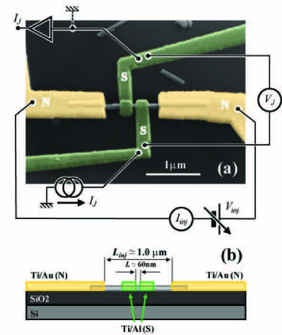
One practical implementation of the present InAs-NW hot-electron Josephson transistor concept is shown in Figure 1a. The SNS junction was fabricated by e-beam lithography starting from an n-doped InAs NW (the N region, for further details see Methods) and comprises two Ti/Al superconducting electrodes placed at a distance (S regions). Control electrodes were fabricated by depositing two additional normal-metal Ti/Au leads at the two ends of the NW. As schematically illustrated by the overlay of Fig. 1a, the N leads are used to drive a dissipative current through the NW thereby tuning Josephson coupling in the S-NW-S structure.
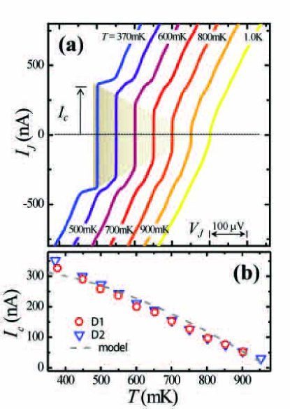
Figure 2a shows a set of typical IV characteristics from one of the measured S-NW-S junctions at equilibrium (i.e., ) and at different bath temperatures . High critical currents up to (corresponding to a supercurrent density ) are observed and Josephson coupling typically persists up to about . Furthermore, from the junction differential-resistance spectra (see Supplementary Materials) we infer a superconducting order parameter and a junction normal-state resistance . The product attains values as large as and indicates the overall success of our junction-fabrication procedure Heikkila . Based on carrier-density and electron-mobility values (see Methods) we estimate a momentum-relaxation length and a diffusion coefficient . Given the junctions geometrical length we can estimate the Thouless-energy value, i.e., the characteristic energy scale of the N region, . These values indicate that our devices can be described within the frame of the diffusive short-junction limit ( and ) Heikkila . Figure 2b shows the evolution of versus at for two representative devices D1 and D2. For comparison, the theoretical prediction for an ideal short diffusive SNS junction Heikkila ; ShortDiffusive is also plotted assuming for both devices a supercurrent suppression of the order of . Such a suppression can be expected and probably mainly stems from a residual barrier at the NW-superconductor contact Heikkila ; Courtois08 ; Garcia09 .
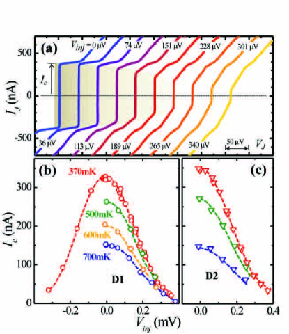
Figure 3 demonstrates operation of the NW hot-electron Josephson transistor: supercurrent can be fully suppressed by the application of a voltage bias of the order of a few hundred across the N control line. The overall evolution of the IV characteristics of device D2 as a function of at is displayed in Fig. 3a. The corresponding monotonic decay and complete suppression of the critical current vs at different bath temperatures is reported in Figs. 3b and 3c for devices D1 and D2, respectively. Our results show that an injection power of barely is sufficient to completely quench the supercurrent.
We emphasize that the observation and control of such a robust Josephson effect is made possible by the chosen device architecture, which allows us to use short SNS junctions while retaining full tunability of the supercurrent flow. In fact there is no fundamental lower limit to in our scheme, while other approaches such as, for instance, Josephson field effect transistors (JoFETs) Doh05 ; Clark80 ; Akazaki96 , require longer junctions to allow electrostatic gating and avoid excessive screening from the electrodes. These requirements lead to larger control voltages, weaker proximity effect and stray capacitance dictated by the integration of strongly-coupled gates on top of short junctions. Clearly the present operational principle is amenable to all-metal implementations. We should like to stress, however, that our NW-based architecture offers a significant beneficial feature, thanks to the resulting higher impedance in the injection line. The latter reduces the required control power by orders of magnitude with respect to what shown so far in comparable metallic systems Morpurgo98 ; Baselmans99 ; Baselmans2001 .
Insight into the working principle of this device can be gained by recalling that in diffusive SNS junctions a continuum spectrum of Andreev bound states is responsible for the supercurrent flow across the structure Wilhelm ; Heikkila . Occupation of these supercurrent-carrying states is determined by the quasiparticle energy distribution in the N region which can, in turn, be controlled through the application of a finite bias across the NW Wilhelm ; Heikkila . Although a detailed quantitative description of this effect is rather complex, we believe that the dominant physics governing our devices can be captured by considering the experimentally-observed heating of the electron system following current injection. Comparison between Figs. 2a and 3a suggests that upon hot-quasiparticle injection NW electrons can be described by a quasi-equilibrium Fermi-energy distribution characterised by a temperature larger than the bath temperature Giazotto06 . Thanks to the experimental data available, we can convert the measured values into by using the measured temperature-calibration data in Fig. 2b, i.e., by exploiting the equilibrium Josephson junction as an electron thermometer Savin04 ; Tirelli08 ; SNSThermo .
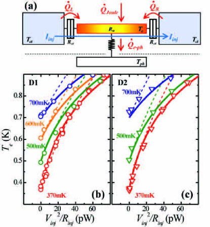
The resulting evolution of the electron temperature is displayed in Fig. 4b and 4c for devices D1 and D2, respectively. values as a function of and are determined by the steady-state thermal balance of several in-coming and out-going heat fluxes within the device system, as sketched in Fig. 4a. In particular, injection of hot carriers and thermal leakage through the lateral N electrodes provide a heat inflow contribution , where the parameter is ideally equal to the Lorentz number and , and represent the voltage drop, the temperature and the contact resistance, respectively. Although current injection in the control line can in principle lead to a temperature gradient along the NW, we assume the latter to be described as lumped resistor characterized by an average electronic temperature . Furthermore, Joule dissipation within the NW itself is taken into account through the additional term , where represents the voltage drop across the NW. These contributions can be recast in terms of the measured injection voltage and total resistance of the injection line by defining the lever arms and with the constraint . Similarly, it is possible to define and . This leads to
| (1) |
where we set . The other main relaxation mechanism which is expected to play a role in our structures is heat exchange between electrons and acoustic phonons () in the NW. To this end we make the simplifying assumption that , which holds for bulk metals at low temperatures (i.e., typically below K), where is a material-dependent constant Giazotto06 , is the NW volume and is the phonon temperature in the nanostructure. Since 70-80% of the NWs are covered by electrodes (see Fig. 1a), we also assume that , i.e., NW phonons thermalize at the Si-substrate and N-lead common bath temperature. Based on all this, we use
| (2) |
to fit the data collected on devices D1 and D2.
Equation (2) well describes the observed behaviour, as visible in Fig. 4b and 4c. is estimated based on transport data on wires of different lengths; we note that its value rescales the extracted best-fitting parameters and , but nevertheless does not modify the best-fit curves. We obtain and , using the NW volume . We note that our estimate of is comparable to values typical of bulk metallic films Giazotto06 . Furthermore, although the term in Eq. 2 cannot properly account alone for the observed behaviour (see dashed lines in Figs. 4b and 4c), the precise relative contribution of lead and phonon thermal leakage is rather delicate to estimate owing to the correlation between the two fitting parameters.
We should finally like to comment on two important figures of merit of the transistor: its power gain and speed of operation. Even if the former is lacking in the present non-optimized devices, it can be made sizable by tuning the ratio between and Wilhelm , i.e. by fabricating sufficiently-long control lines. Concerning speed, switching time is determined by how fast an out-of-equilibrium electron energy distribution can be established in the NW Morpurgo98 ; Giazotto04 ; in our case we estimate , which can be decreased by shortening or increasing .
In light of possible applications, the present InAs NW-based hot-electron Josephson transistor concept offers a number of attracting features: (i) a large, yet tunable, critical supercurrent; (ii) the possibility to achieve large power gains in optimized devices; (iii) a high operating frequency (easily up to GHz); (iv) a reduced dissipation ( pW or below), ideal for low-temperature applications; (v) the possibility to combine the Josephson effect with custom quantum structures defined during the NW growth. The adoption of self-assembled nanostructures as the core element of this class of devices thus paves the way to rather broad opportunities since it allows the design and growth of epitaxial quantum systems characterized by atomically-defined potential profiles Roddaro08 ; Jiang07 , a crucial element for several innovative out-of-equilibrium nanodevice schemes Giazotto06 ; Tirelli08 ; Linke09 .
We gratefully acknowledge R. Fazio, H. Linke, J. Matthews, F. Taddei and H. Xu for fruitful discussions. The work for partially supported by the INFM-CNR Seed projects “Acoustoelectrics on Self-Assembled One-dimensional Semiconductors” and “Quantum-Dot Refrigeration: Accessing the K Regime in Solid-State Nanosystems”, and by the NanoSciERA project “NanoFridge”.
I METHODS
Fabrication details of InAs NW devices and measurement set-up. Selenium doped NWs were grown by chemical beam epitaxy on a InAs 111B substrate. Gold catalyst particles were formed by thermal dewetting (at 520∘C for 20 min) of a 0.5 nm thick Au film under TBA flux. NWs were grown for 2 hours at using TBA (), TMI () and DTBSe (). NWs had typically a diameter and length . Transport parameters were estimated over an ensemble of nominally identical m-long NW field effect transistors using a charge control model Jiang07 and a numerical evaluation of the gate capacitance. Carrier density was estimated to be and electron mobility . Hot-electron Josephson transistors were fabricated using a technique of dry cleavage of the NWs onto Si/SiO2 substrates ( oxide on intrinsic Si). Contacts were obtained by a two-step aligned process: thermal evaporation of Ti/Au () was performed first and followed by e-beam deposition of Ti/Al (). In order to obtain transparent metal-NW contacts great care was devoted to the passivation of the semiconductor surface : InAs NWs were treated with a NH4Sx solution before each evaporation step. The electric characterization was performed by cooling the devices in a filtered 3He refrigerator down to about . Current injection at the normal contacts was obtained using a floating biasing source. Currents and voltages were measured using room-temperature preamplifiers.
Theoretical model for a diffusive SNS Josephson junction in the short limit. The measured Josephson critical currents were analyzed by using a model which holds for short diffusive SNS junctions. In this regime the critical supercurrent is expected to scale with the temperature as Heikkila ; ShortDiffusive
where , , and is a phenomenological suppression coefficient which accounts for the non-ideality of the junction Courtois08 ; Garcia09 . In the above equation, is the Boltzmann constant, is the electron charge, is the normal-state resistance of the junction, is the superconducting order parameter, and is the macroscopic phase difference across the SN boundaries.
II Supplementary materials
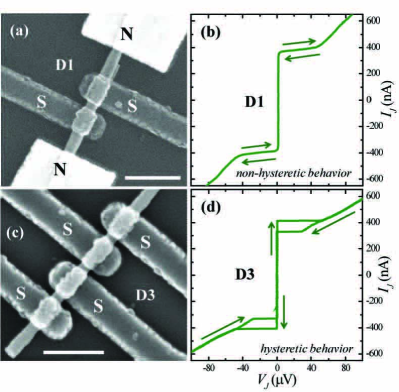
Metallic contacts play a crucial role in thermal sinking of the NW device Giazotto06 . Figure S1 shows the different behaviour observed on Josephson NW transistors containing either both N and S contacts (Fig. S1 a), or only S ones (Fig. S1 c). In the first case (see Fig. S1 b) we never observed hysteresis in the IV characteristics, while in the second case (see Fig. S1 d) a clear hysteresis developed for devices which exhibit exceeding . This different behaviour, which was verified on a number of devices, can be ascribed to the poor thermal conductivity of the superconducting leads in good metallic contact with the NW which act as Andreev mirrors for what concerns electronic heat conduction Giazotto06 . Hysteresis in mesoscopic SNS junctions is believed to stem from electron heating of the N region once the junction switches to the resistive branch Courtois08 . Our data suggest that the device in Fig. S1c heats up more than that in Fig. S1a when it switches to the dissipative regime.
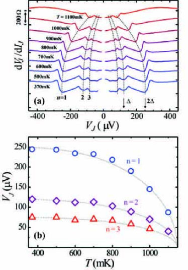
The differential resistance spectra versus voltage of a typical Josephson NW transistor with all-superconducting leads is visible in Fig. S2a. The plot shows multiple Andreev reflection features Octavio83 occurring at values with , , and for a sequence of different bath temperatures. The extracted value of the gap parameter is . The position of the minima in as a function of the temperature (see Fig. S2b) closely follows the Bardeen-Cooper-Schrieffer prediction for the superconducting gap Tinkham .
References
- (1) P. G. de Gennes, Superconductivity of Metals and Alloys (W. A. Benjamin, 1966).
- (2) A. F. Andreev, Sov. Phys. JETP 19, 1228 (1964).
- (3) K. K. Likharev, Rev. Mod. Phys. 51, 101 (1979).
- (4) C. M. Lieber MRS Bulletin 28, 486?491 (2003).
- (5) M. T. Björk, B. J. Ohlsson, T. Sass, A. I. Persson, C. Thelander, M. H. Magnusson, K. Deppert, L. R. Wallenberg, and L. Samuelson, Nano Lett. 2, 87 (2002).
- (6) S. Roddaro, A. Fuhrer, P. Brusheim, C. Fasth, H. Q. Xu, L. Samuelson, J. Xiang, C. M. Lieber, Phys. Rev. Lett. 101, 186802 (2008).
- (7) E. A. Hoffmann, H. A. Nilsson, J. E. Matthews, N. Nakpathomkun, A. I. Persson, L. Samuelson, and H. Linke, Nano Lett. 9, 779 (2009).
- (8) J. Xiang, A. Vidan, M. Tinkham, R. M. Westervelt, C. M. Lieber, Nat. Nanotechnol. 1, 208 (2006).
- (9) J. van Dam, Y. Nazarov, E. Bakkers, S. De Franceschi, L. Kouwenhoven, Nature 442, 667 (2006).
- (10) Y.-J. Doh, J. A. van Dam, A. L. Roest, E. P. A. M. Bakkers, L. P. Kouwenhoven, and S. De Franceschi, Science 309, 272 (2005).
- (11) R. Frielinghaus, I. E. Batov, M. Weides, H. Kohlstedt, R. Calarco, and Th. Schäpers, preprint arXiv:1001.2380v1.
- (12) T. Sand-Jespersen, J. Paaske, B. M. Andersen, K. Grove-Rasmussen, H. I. Jørgensen, M. Aagesen, C. B. Sørensen, P. E. Lindelof, K. Flensberg, and J. Nygård, Phys. Rev. Lett. 99, 126603 (2007).
- (13) F. K. Wilhelm, G. Schøn, and A. D. Zaikin, Phys. Rev. Lett. 81, 1682 (1998).
- (14) A. F. Morpurgo, T. M. Klapwijk, and B. H. van Wees, Appl. Phys. Lett. 72, 966 (1998).
- (15) Th. Schäpers, J. Malindretos, K. Neurohr, S. Lachenmann, A. van der Hart, G. Crecelius, H. Hardtdegen, H. Lüth, and A. A. Golubov, Appl. Phys. Lett. 73, 2348 (1998).
- (16) J. J. A. Baselmans, A. F. Morpurgo, B. J. van Wees, and T. M. Klapwijk, Nature 397, 43 (1999).
- (17) A. M. Savin, J. P. Pekola, J. T. Flyktman, A. Anthore, and F. Giazotto, Appl. Phys. Lett. 84, 4179 (2004).
- (18) F. Giazotto, T. T. Heikkilä, F. Taddei, Rosario Fazio, J. P. Pekola, and F. Beltram, Phys. Rev. Lett. 92 137001 (2004).
- (19) M. S. Crosser, P. Virtanen, T. T. Heikkilä, and N. O. Birge, Phys. Rev. Lett. 96 167004 (2006).
- (20) S. Tirelli, A. M. Savin, C. Pascual Garcia, J. P. Pekola, F. Beltram, and F. Giazotto, Phys. Rev. Lett. 101, 077004 (2008).
- (21) F. Giazotto, T. T. Heikkilä, A. Luukanen, A. M. Savin, J. P. Pekola, Rev. Mod. Phys. 78, 217 (2006).
- (22) T. T. Heikkilä, J. Särkkä, and F. K. Wilhelm, Phys. Rev. B 66, 184513 (2002).
- (23) I. O. Kulik and A. N. Omelyan’chuk, Fiz. Nizk. Temp 4, 296 (1978) [Sov. J. Low Temp. Phys. 4, 142 (1978)].
- (24) H. Courtois, M. Meschke, J. T. Peltonen, and J. P. Pekola, Phys. Rev. Lett. 101, 067002 (2008).
- (25) C. Pascual García and F. Giazotto, Appl. Phys. Lett. 94, 132508 (2009).
- (26) T. D. Clark, R. J. Prance, A. D. C. Grassie, J. Appl. Phys. 51, 2736 (1980).
- (27) T. Akazaki, H. Takayanagi, J. Nitta, and T. Enoki, Appl. Phys. Lett. 68, 418 (1996).
- (28) J. J. A. Baselmans, B. J. van Wees, and T. M. Klapwijk, Phys. Rev. B 63, 094504 (2001).
- (29) M. Meschke, J. T. Peltonen, H. Courtois, and J. P. Pekola, J. Low Temp. Phys. 154, 190 (2009).
- (30) X. Jiang, Q. Xiong, S. Nam, F. Qian, Y. Li, and C. M. Lieber, Nano Lett. (2007).
- (31) M. Octavio, M. Tinkham, G. E. Blonder, and T. M. Klapwijk, Phys. Rev. B 27,6739 (1983).
- (32) M. Tinkham, Introduction to Superconductivity, 2nd Edn. (McGraw-Hill, 1996).