Shot noise suppression at room temperature in atomic-scale Au junctions
Abstract
Shot noise encodes additional information not directly inferable from simple electronic transport measurements. Previous measurements in atomic-scale metal junctions at cryogenic temperatures have shown suppression of the shot noise at particular conductance values. This suppression demonstrates that transport in these structures proceeds via discrete quantum channels. Using a high frequency technique, we simultaneously acquire noise data and conductance histograms in Au junctions at room temperature and ambient conditions. We observe noise suppression at up to three conductance quanta, with possible indications of current-induced local heating and noise in the contact region at high biases. These measurements demonstrate the quantum character of transport at room temperature at the atomic scale. This technique provides an additional tool for studying dissipation and correlations in nanodevices.
Mechanical break junctions have proven to be an invaluable tool in understanding the physics of electronic conduction in metals at the atomic scaleAgrait:2003 . By bringing two metals in and out of contact while simultaneously performing electrical measurements, it is possible to build up a histogram of conductance values that occur when the contact between the electrodes ranges from tunneling to the few-atom level. In metals with -like conduction electrons, well-defined peaks in conductance histograms near integer multiples of the quantum of conductance () frequently appear. These are now interpreted as a signature of conductance quantization, transport of electrons through an integer number of (ideally) perfectly transmitting quantum channels.
The break junction approach has recently been extended to examine ensemble-averaged conduction in single-molecule junctionsXiao:2004 ; Gruter:2005 ; Venkataraman:2006 . The ability to acquire such histograms at room temperature at relatively high rates has greatly advanced studies of molecular conduction, permitting systematic studies of the effects of contact functionalizationChen:2006 ; Park:2007 , molecular lengthVenkataraman:2006 , and molecular conformationVenkataraman:2006b . However, from the conductance alone, it is generally not possible to determine whether particular peaks in conductance histograms are the result of quantized electronic transport through well-defined quantum channels, or whether these peaks simply indicate particularly stable junction configurations.
The mapping of conductance into transmission coefficients for discrete quantum electronic channels requires additional information beyond the linear conductance. Two approaches have been pursued at cryogenic temperatures to infer the quantum nature of conduction in such junctions. Sub-gap structure in superconducting point contactsScheer:1998 is one means of identifying the number of transmitting channels and their particular transmission coefficients. Alternately, one may use shot noise to examine the same physics. Shot noise results from the discrete nature of the electronic charge. In shot noise, the mean square current noise per Hz is related to , the average DC current, as . Here is the electronic charge, and is the Fano factor. In the classical Poissonian limit, .
The Fano factor is modified in the limit of quantum transport, when for a quantum channel , electrons are transmitted and reflected with respective probabilities, and . The resulting full expression for current noise at finite temperature in the absence of inelastic effects isBlanter:2000
| (1) |
These terms include both the Nyquist-Johnson noise and shot noise contributions. This is expected to be valid at frequencies much smaller than and , and voltages smaller than the characteristic energy scales over which the vary. As is clear from Eq. (1), in the limit of a small number of channels, one expects strong suppression of noise when channels are fully transmitting (). Shot noise is further suppressed in macroscopic conductors due to inelastic electron-phonon scattering, which effectively “smears” electrons out across multiple channelsBlanter:2000 .
Following groundbreaking work in semiconductor quantum point contactsReznikov:1995 ; Kumar:1996 , low temperature (4.2 K) measurements of shot noise in Au break junctionsvandenBrom:1999 have found shot noise suppression near integer conductance values, demonstrating that the conductance quantization observed in those experiments does result from fully transmitting channels. More recent measurementsDjukic:2006 have used shot noise to infer the transmission coefficients in the dominant channels in transport through single deuterium molecules. In these experiments noise is measured using a low bandwidth approach involving cross-correlation of voltage amplifiers, necessitating very stable junctions for the comparatively slow acquisition.
Here we present measurements of noise in Au breakjunctions acquired at room temperature using a high frequency approach coincident with conductance measurements. We observe peaks in conductance histograms at the roughly 1, 2, and 3, as expected for this material. The averaged noise shows suppression at precisely the same conductance values as the peaks in the conductance histograms. This demonstrates that the quantum mechanical suppression of noise due to fully transmitting contacts survives even at room temperature, where inelastic processes are much stronger than in previous low temperature experiments. We discuss the measurement technique and its limitations, including indications of possible contributions and Joule heating-induced Johnson noise. These experiments raise the possibility of performing room temperature shot noise measurements in single molecules.
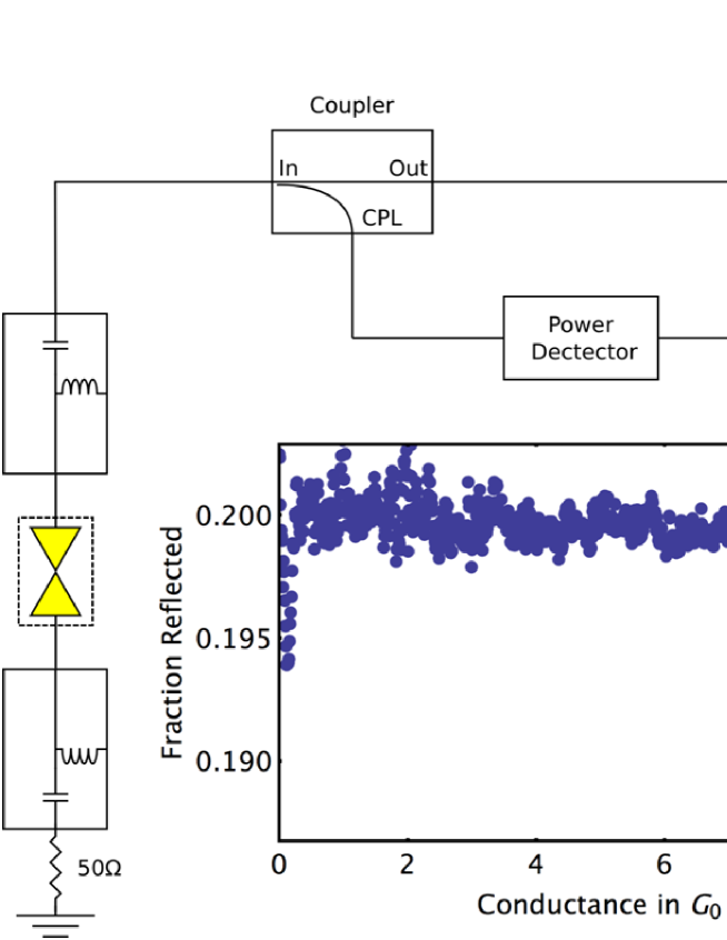
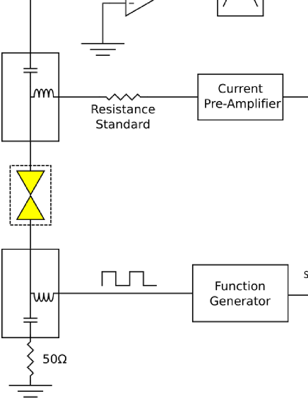
Figure 1 shows a schematic of the measurement setup. A mechanical break junction is formed using a notched gold wire mounted on metal shim-stock. A computer-controlled piezo motor is used to flex the substrate, bringing the ends of the gold wire repeatedly in and out of contact. These measurements are performed under ambient conditions at room temperature. First we consider the “DC” portion of the measurement circuit. To determine the conductance, a function generator sources an offset square wave of desired amplitude so that the applied voltage oscillates between zero and a set value, . This voltage is passed into the junction via the “DC” input of a bias-tee. The frequency of the square wave is typically below 10 kHz, a bound set by the properties of the bias-tee used to deliver the voltage to the junction. The other side of the junction is connected through a current-limiting resistance standard (General Radio 1433-G Decade Resistor) to a Keithley 428-PROG current amplifier. The resistance standard is used to avoid overloading the current amplifier input stage when the junction is in a fully shorted high conductance configuration. The output of the current amplifier is measured using a lock-in amplifier synchronized to the input square wave, with a typical lock-in output time constant of 1 ms.
The shot noise measurement relies on the high frequency response of the circuit, which is very different from that at DC. The bias-tees play a crucial role here. The side of the junction that is biased at DC via the function generator is terminated at 50 at high frequencies. Similarly, at high frequencies the other bias-tee isolates the other side of the junction from the resistance standard and the current preamplifier. Instead, that side of the junction is coupled via an extremely short (few cm) piece of 50 coaxial cable directly to the input of the RF amplifier chain with a nominal gain of 70 dB, followed by filters that define a nominal bandwidth extending from 250 to 520 MHz. The RF signal is then passed to a power meter with an output proportional to the logarithm of the incident RF power. The output of this RF power meter is detected using a second lock-in amplifier also synchronized to the input square wave, with a lock-in output time constant of 1 ms.
Note that one cannot think of the RF circuit in quasi-DC terms, with the resistance of the junction and the stray capacitance forming an RC divider that suppresses all high frequency response. Instead one must consider the junction as a source of mean square current fluctuations, , in parallel with some characteristic impedance, , determined by resistive and reactive components. As explained in the Supporting Information, one end of the junction is terminated at 50 , and the terminated junction acts as an equivalent noise source with an effective impedance . This “generator” is then connected to a very short piece of transmission line to a nominally 50 amplifier chain. While maximal power transfer would require , power is still delivered to the amplifier chain even when there is an impedance mismatch. If , the power transferred to the amplifier chain is approximately . At any given frequency within the nominal bandwidth of the RF system, one can measure the effects of the impedance mismatch by measuring the reflection properties of the junction. Ideally one wants to do this simultaneously with data acquisition, across the whole bandwidth, but that is not practical, and that data is acquired separately.
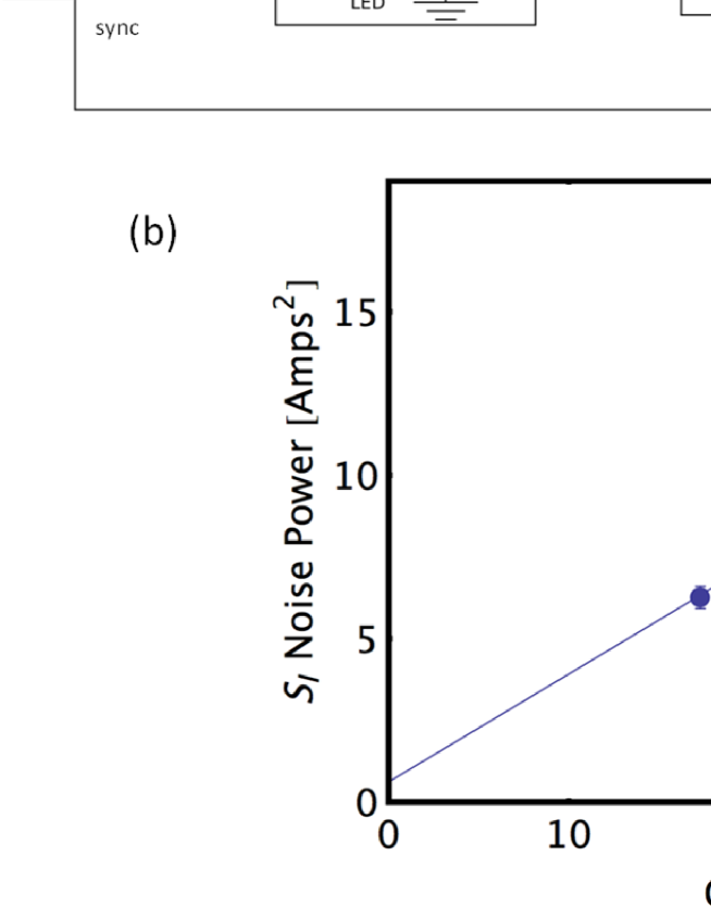
We demonstrate that this approach is capable of measuring shot noise in a system with a high DC impedance, provided the RF properties are calibrated. As shown in Fig. 2, we have use the same amplifier system to measure the shot noise produced by a vacuum photodiode. The photodiode cathode is biased through a bias-tee to -45 V using a DC power supply, while the RF port of the cathode bias-tee is terminated at 50 . The anode is connected through the DC terminal of a bias-tee to the current amplifier and subsequent lock-in. The RF port of the anode bias-tee is then connected to the amplifier chain. A light-emitting diode (LED) is driven by the square wave output of a function generator to illuminate the photodiode. The current amplifier measures the (quasi-DC when LED is on) photocurrent. The RF amplifier chain amplifies the noise power, which is then measured by the power meter. Lock-in detection (synced to the LED illumination) is then used to find the noise power produced by the photocurrent.
Depending on illumination level, the DC differential resistance of the vacuum photodiode around the operating point ranges from 28 to 205 M. However, the RF properties of the photodiode rather than this DC resistance determine the power transfer of the shot noise to the amplifier chain. As described in the Supporting Information, a reflectometry measurement of the cathode-terminated photodiode from the anode side is sufficient to characterize this power transfer, via a frequency-dependent reflection coefficient, .
Conversion of the measured noise power into units of current noise per unit bandwidth requires knowledge of both and the gain-bandwidth product, , of the amplifier chain. An RF source is cycled through 1000 evenly spaced frequencies, , from 1 MHz to 1 GHz, feeding an input power, dbm, into the amplifier chain. The output of the amplifier chain, is recorded at each frequency, as is the background, output with set to zero. The gain-bandwidth product is then computed by numerical integration:
| (2) |
A separate measurement of of the photodiode at each frequency (see Supporting Information) allows us to correct for the division of power between the photodiode and the amplifier chain. The measured noise power is then divided by this corrected gain-bandwidth product to infer the power noise per Hz delivered to the amplifier chain. Finally this is then divided by the input impedance of the first stage amplifier, 50 , to obtain the current noise per Hz produced by the photodiode. As shown, this noise scales linearly with the photocurrent, with a slope of Amps/Hz. This compares well with expectations, deviating from the expected by less than 3%. This demonstrates that the RF approach can successfully measure shot noise, even though the DC resistance of the photodiode is much greater than 50 .
In the break junction case, lock-in detection of the RF power is crucial, since at 300 K the Nyquist-Johnson equilibrium noise is significant. Neglecting quantum effects, the Nyquist-Johnson current noise of a 1 conductor at 300 K is A2/Hz, while (for ) the current shot noise at a DC current of 1 A would be A2/Hz. Without lock-in detection, the shot noise would barely be detectable above the thermal noise at a DC bias voltage exceeding 100 mV. Even with phase-sensitive detection there is some background RF noise power even at . This background is strongly reduced when great care is taken on shielding extraneous interference. While the logarithmic power meter allows noise measurements over a large dynamic range, it is particularly sensitive to background noise, compared with a linear power detector. As we discuss further below, lock-in detection of the noise power avoids contributions from the equilibrium thermal noise; however, heating and resultant temperature changes due to the applied DC bias would be detected in this approach. Thus, the measured noise power is likely a combination of shot noise and bias-induced-heating changes in the Nyquist-Johnson noise. An additional possible contribution due to “flicker” noise will be discussed below.
The reflection coefficient measurement is considerably more challenging for the break junction case. In principle one would like to measure at frequencies across the RF bandwidth on-the-fly. In practice, one can acquire histograms of as a function of at a series of discrete frequencies. Doing this densely across the whole frequency range of interest is laborious and difficult. Measurements indicate (see SI) that at individual frequencies, is essentially independent of for conductances between and 5 . In the break junction data presented here we choose to plot the noise in “arbitrary units”, accepting that our incomplete knowledge of constitutes a systematic error (independent of from 0.5 to 5 ) in the overall magnitude of the noise.
Conductance and noise data are recorded simultaneously as the junction is brought into and out of contact, using a DAQ system to sample the lock-in outputs at 1k samples/s. Histograms of the measured conductance values are compiled in real time during junction breaking and formation. Simultaneously, running averages of the noise power are computed for each conductance bin. The data analysis is entirely automated, with no post-selection of “nice” traces. In general, conductance histograms were cleaner, with more observable conductance quanta, during junction breaking rather than formation.
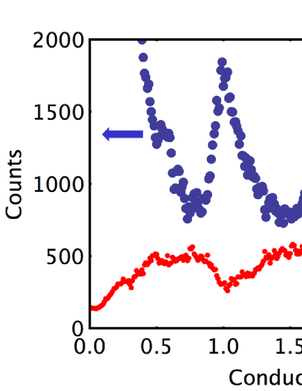
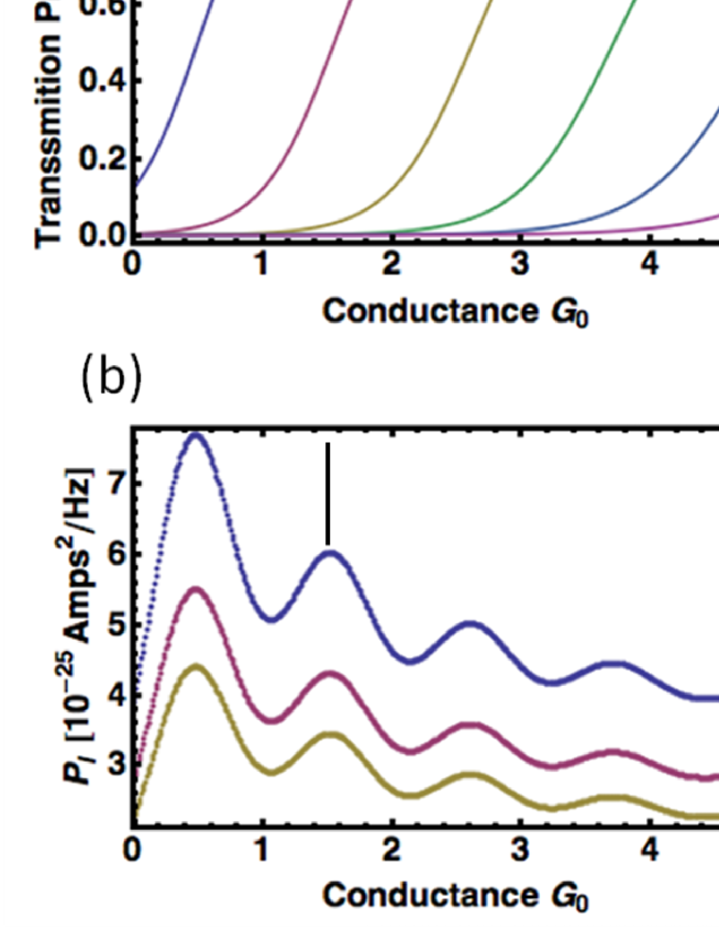
Figure 3 shows an example data set, acquired at room temperature over the course of several hours. The conductance histogram clearly shows peaks at approximately 1, 2, and 3 , as expected from previous work on Au junctionsVenkataraman:2006 . Deviations from perfect quantization at integer multiples are seen in some samples, but are always quantitatively consistent with previous measurements on Au junctions at room temperature in the presence of work hardeningYanson:2005 . The averaged noise power distribution shows significant dips in power centered at precisely the conductance values associated with peaks in the histogram. This noise suppression is very similar to that seen by van den Brom et al. at liquid helium temperaturesvandenBrom:1999 . Note that the suppression is not expected to reach all the way to , since statistically junctions with may be formed in many ways, with many possible combinations of for different channels.
As described by van den Brom and van RuitenbeekvandenBrom:1999 , one can construct an explicit model of the expected shot noise by assuming a form for the contributions of different conductance channels as a function of conductance. This is likely to be reasonable only in the small number of channels limit. Figure 4a shows such a model, while Fig. 4b plots the corresponding expected shot noise, based on Eq. (1), for different magnitudes of DC (square-wave) bias. The calculations assume a temperature of 300 K, and take into account that the actual voltage dropped across the junction is , where is the resistance standard, approximately 6 k for the measurements in Figs. 3 and 4c.
There is considerable interest in comparing data sets taken at different junction biases. Higher biases enable possible inelastic processes such as optical phonon scattering, and there are theoretical predictionsChen:2003 ; Chen:2005 (particularly in molecular junctionsMitra:2004 ; Koch:2005 ) that such processes can modify the Fano factor away from the prediction of Eq. (1). Magnetic processes can also lead to unconventional Fano factor valuesSela:2006 . The calculation shown in Fig. 4b assumes no such modifications.
Figure 4c shows averaged measured noise power as a function of conductance for the same magnitudes as in the model of Fig. 4b. No background subtraction has been performed, and as above no correction has been made to the noise data to account for the dependence of of the junction on the conductance.
Comparison between the model and the data reveals several features of interest. The overall trend at high conductances toward lower noise with increasing is expected due to the resistance standard: When , the DC current approaches , and the DC voltage, , relevant for Eq. (1) becomes small because most of the applied DC voltage is dropped across the resistance standard. The deviation of the data from the model at low conductances () is not surprising, given the sensitivity of that data to the reflection coefficient resulting from the impedance mismatch between the junction and the amplifier chain.
One must be concerned about contributions to the data due to noise. In electronic conduction this noise results from temporal fluctuations of the resistance, with a broad distribution of characteristic timescalesDutta:1981 ; Weissman:1988 . This noise has been shown to exist in metal contacts approaching the atomic scaleWu:2008 . Static conductance fluctuations as a function of DC bias voltage across nanojunctions are known to be suppressed near quantized conductance valuesLudoph:1999 . It is conceivable that the time-dependent conductance fluctuations that give rise to noise could be similarly affected by the decreased backscattering and increased junction stability near quantized conductance values. To test for this physics, we consider the dependence of the measured noise on the DC current through the junction. At a given , conductance fluctuation noise is expected to be quadratic in the DC current, in contrast to shot noise. We do not see strong signatures of such a dependence, as shown in Fig. 4d, finding that the measured noise is roughly linear in DC current, extrapolating toward a finite background value at zero current. There is some nonlinearity, however, meaning that some contribution from noise cannot be completely ruled out.
The presence of noise suppression at room temperature demonstrates explicitly the quantum character of transport in these atomic-scale devices. Inelastic processes such as electron-phonon scattering can remove energy from the “hot” electron system and redistribute electrons between the different quantum channels. This is what leads to the suppression of shot noise in macroscopic conductors at room temperature. These data suggest that such inelastic processes operate on length scales longer than the single-nanometer junction size, even at 300 K and biases in the tens of mV range.
An additional contribution to the superlinearity seen in Fig. 4d that must be considered is bias-driven local electronic heating of the junction. Such heating would be synchronous with the bias current, and thus would be detected in the lock-in technique. Bias-driven ionic heating has been inferred in such junctions previously by studying the bias-dependence of the junction breaking processTsutsui:2007 . It has also been noted that effective temperature changes in robust junctions can reach several hundred Kelvin at biases of a few hundred mVWard:2008 . An effective increase in the electronic temperature (which is relevant to Eq. (1) would not have to be very large to be detectable. The plausibility of this explanation is reinforced by the vertical line shown in Fig. 4b, indicating the change in Nyquist-Johnson current noise expected for an electronic temperature change at that conductance of 20 K.
Such electron heating has been considered theoretically in some detailChen:2003 ; Chen:2005 ; DAgosta:2006 . In fact, the authors of Ref. DAgosta:2006 explicitly suggest using measurements of the noise as a means of detecting local, nonequilibrium heating in atomic-scale contacts. Detailed modeling of the local junction temperature is complicated by the fact that local Joule heating and effective thermal path are explicit and implicit functions, respectively, of . Such modeling is beyond the scope of the present paper and will be examined carefully in a later publication.
This technique raises the possibility of performing rapid assays of shot noise through molecules, given the great progress that has been made in recent molecular break junction conductance measurements. As mentioned above, both electron-vibrational effects and magnetic processes are predicted to modify Fano factors away from . However, small molecule conductances tend to be on the order of . Such low conductance junctions have, necessarily, very poor impedance matching to the usual 50 RF electronics used in the noise measurements. Moreover, there is great interest in examining noise in such systems at much lower bias currents. Improved coupling of junction noise power to the amplifiers and reduced backgrounds would be a necessity. Impedance matching networks or tank circuits may provide a means of adapting this approach to the molecular regime, though not without a likely reduction in bandwidth.
We have used high frequency methods to observe shot noise suppression in atomic-scale Au contacts at room temperature, demonstrating clearly the quantum character of conduction in these nanodevices. High frequency methods allow the rapid acquisition of noise data simultaneously with statistical information about conduction in ensembles of junctions. A slightly nonlinear dependence of the measured noise on DC bias current raises the possibility that local heating and noise may need to be considered in these structures. While impedance matching for low conductance junctions is a challenge, the prospect of adapting this approach to study noise in molecular junctions is appealing.
DN and PJW acknowledge support from Robert A. Welch Foundation Grant C-1636 and NSF grant DMR-0855607.
References
- (1) Agrait N.; Levy Yeyati, A.; van Ruitenbeek, J. M. Phys. Rep. 2003, 377 81-279.
- (2) Xiao, X. Y.; Xu, B. Q.; Tao, N. J. Nano Lett. 2004, 4, 267-271.
- (3) Grüter, L.; Cheng, F.; Heikkilä, T. T.; González, M. T.; Diederich, F.; Schönenberger, C.; Calame, M. Nanotech. 2005, 16, 2143-2148.
- (4) Venkataraman, L.; Klare, J. E.; Tam, I. W.; Nuckolls, C.; Hybertsen, M. S.; Steigerwald, M. L. Nano Lett. 2006, 6, 458-462.
- (5) Chen, F.; Li, X. L.; Hihath, J.; Huang, Z. F.; Tao, N. J. J. Am. Chem. Soc. 2006, 128, 15874-15881.
- (6) Park, Y. S.; Whalley, A. C.; Kamenetska, M.; Steigerwald, M. L.; Hybertsen, M. S.; Nuckolls, C.; Venkataraman, L. J. Am. Che. Soc. 2007, 129, 15768-15769.
- (7) Venkataraman, L.; Klare, J. E.; Nuckolls, C.; Hybertsen, M. S.; Steigerwald, M. L. Nature 2006, 442, 904-907.
- (8) Scheer, E.; Agrait, N.; Cuevas, J. C.; Levy Yeyati, A.; Ludoph, B.; Martin-Rodero, A.; Bollinger, G. R.; van Ruitenbeek, J.; Urbina, C. Nature 1998, 394, 154-157.
- (9) Blanter, Y. M.; Büttiker, M. Phys. Rep. 2000, 336, 1-166.
- (10) Reznikov, M.; Heiblum, M.; Shtrikman, H.; Mahalu, D. Phys. Rev. Lett. 1995, 75, 3340-3343.
- (11) Kumar, A.; Saminadayar, L.; Glatti, D. C.; Jin, Y.; Etienne, B. Phys. Rev. Lett. 1996, 76, 2778-2781.
- (12) van den Brom, H. E.; van Ruitenbeek, J. M. Phys. Rev. Lett. 1999, 82, 1526-1529.
- (13) Djukic, D.; van Ruitenbeek, J. M. Nano Lett. 2006, 6, 789-793.
- (14) Yanson, I. K.; Shklyarevskii, O. I.; Csonka, Sz.; van Kempen, H.; Speller, S.; Yanson, A. I.; van Ruitenbeek, J. M. Phys. Rev. Lett. 2005, 95, 256806.
- (15) Chen, Y.-C.; Zwolak, M.; Di Ventra, M. Nano Lett. 2003, 3, 1691-1694.
- (16) Chen, Y.-C.; Di Ventra, M. Phys. Rev. Lett. 2005, 95, 166802.
- (17) Mitra, A.; Aleiner, I.; Millis, A. J. Phys. Rev. B 2004, 69, 245302.
- (18) Koch, J.; von Oppen, F. Phys. Rev. Lett. 2005, 94, 206804.
- (19) Sela, E.; Oreg, Y.; von Oppen, F.; Koch, J. Phys. Rev. Lett. 2006, 97, 086601.
- (20) Dutta, P.; Horn, P.M. Rev. Mod. Phys. 1981, 53, 497-516.
- (21) Weissman, M. B. Rev. Mod. Phys. 1988, 60, 537-571.
- (22) Wu, Z.; Wu, S.; Oberholzer, S.; Steinacher, M.; Calame, M.; Schönenberger, C. Phys. Rev. B 2008, 78, 235421.
- (23) Ludoph, B.; Devoret, M. H.; Esteve, D.; Urbina, C.; van Ruitenbeek, J. M. Phys. Rev. Lett. 1999, 82, 1530-1533.
- (24) Tsutsui, M.; Taniguchi, M.; Kawai, T. Nano Lett. 2008, 8, 3293-3297.
- (25) Ward, D. R.; Halas, N. J.; Natelson, D. Appl. Phys. Lett. 2008, 93, 213108.
- (26) D’Agosta, R.; Sai, N.; Di Ventra, M. Nano Lett. 2006, 6, 2935-2938.
Supporting Information
This document contains supporting information regarding RF measurements of shot noise reported in the above manuscript.
I RF equivalent circuits
As shown in Fig. S5a, one should think of a noise source (either a break junction or a vacuum photodiode, in the cases considered here) as an ideal current source of mean square current fluctuations in parallel with an impedance that depends on frequency. The actual noise source is a two-port device at RF, terminated at one end by . The equivalent circuit parameters for the resulting single-port “generator” are then
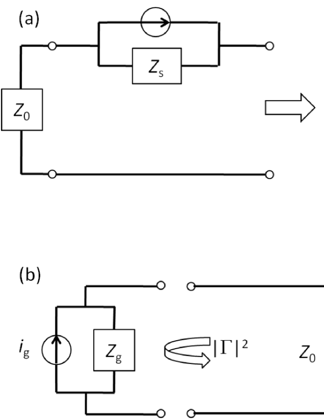
One then considers attaching this generator to a transmission line (characteristic impedance ) and the RF amplifier chain (also ). The current delivered to the load is , and the power transferred to the load is then
If one considered a reflectance measurement looking from a 50 line into the generator (Fig. S5b), one would find
Thus, the power transferred to the load is . In the limit that , .
II Photodiode measurements
Fig. S6 shows the circuit configurations used to measure the reflection coefficient of the terminated vacuum photodiode.

Fig. S7 shows the circuit configurations used to measure the gain-bandwidth product of the nominally 50 amplifier chain. Gain was measured by comparing output power referenced to a known input power for 1000 discrete frequencies across the bandwidth of interest.
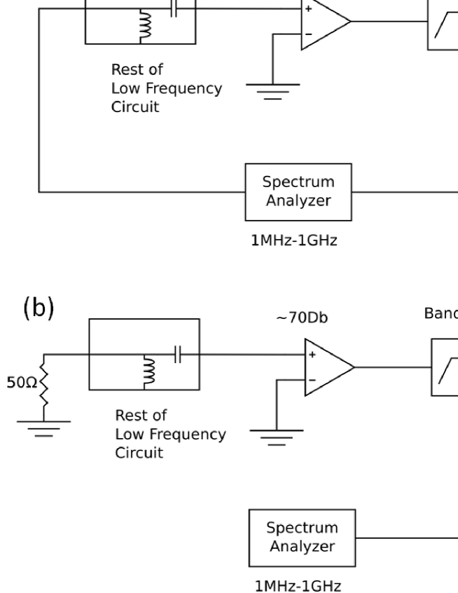
Fig. S8a is the measured gain as a function of frequency for the amplifier chain and filters. Fig. S8b shows the measured fraction of reflected power, , for the photodiode over the same frequency range, obtained with the approach in Fig. S6. Fig. S8c shows the convolution of the gain-bandwidth product and . As shown in the previous section, this convolution may be used to infer the original mean square current fluctuations, , from the photodiode noise source. The results of this procedure are shown in Fig. 3 of the main manuscript text.
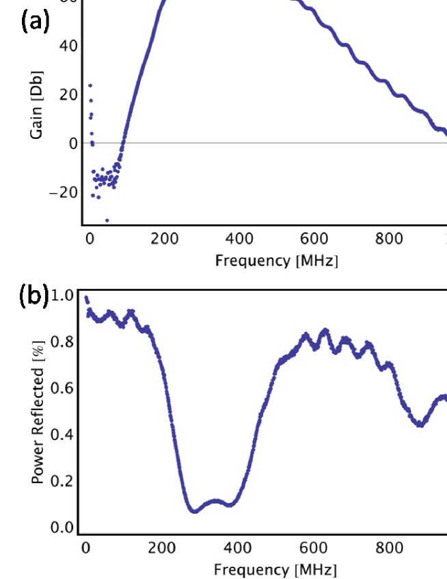
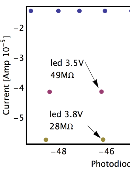
Fig. S9 shows DC current-voltage characteristics of the photodiode around its DC operating point (-45 V) for three of the illumination levels (labeled by the voltages applied to the illuminating LED) used in the photodiode shot noise measurements. The DC resistance is always much larger than 50 , but as explained in the main text, this is irrelevant to the measurements at hand. What does matter is the RF response of the terminated photodiode, and as the data demonstrate, the impedance mismatch over the bandwidth of interest is not nearly as severe as one would infer from purely DC measurements.
III Reflection measurements with break junctions
Figure S10 shows the circuit configuration for reflectance measurements on the break junctions, as well as the data for as a function of for a single frequency, 300 MHz. As discussed in the main text, performing such measurements at many discrete frequencies across the full bandwidth is very tedius. The main point to observe here is that is essentially independent of when .