CALICE Report to the DESY Physics Research Committee
Abstract
We present an overview of the CALICE activities on calorimeter development for a future linear collider. We report on test beam analysis results, the status of prototype development and future plans.
1 Introduction
The CALICE collaboration pursues the development of highly granular calorimeters for a future e+e- linear collider, based on the particle flow approach for optimal overall detector performance.
The collaboration consists of 57 institutes from 17 countries in Africa, America, Asia and Europe and has 336 physicists and engineers as members. Since the last review in 2007, the following institutes joined the collaboration: Tsinghua University, Beijing, University of Bergen, CERN, Kyungpook National University, Daegu, University of Kansas, University of Louvain, Max-Planck-Institute of Physics, Munich, University of Rabat and Casablanca, University of Tsukuba, University of Wuppertal.
We follow different technological options for electromagnetic and hadronic calorimeters in each case. Most of them are candidates for both particle flow based ILC detector concepts, ILD and SiD, and for a detector at a multi-TeV linear collider such as CLIC. Our aim is to cover an as broad as possible range of options with prototypes and test them in particle beams, thereby maximizing the use of common infrastructures like mechanical devices, ASIC architecture or DAQ systems. We work as much as possible in a common software and analysis framework, in order to ease combination and comparison of test beam data, and to achieve a common understanding of strengths and weaknesses of the options under consideration.
The major part of the effort is focused towards presenting realistic proposals for the detector concept reports of the ILC technological design phase 1, which is due in 2012. This is closely coordinated with the detector concept groups. Realistic proposals must have the performance established in test beams, and the designs must demonstrate the scalability towards a full detector and provide estimates for dead regions occupied by services and support, as well as a solid basis for costing. Given the yet uncertain schedule and energy range of the future collider, we also pursue developments which reach a similar maturity only at a later stage.
The development of calorimeter prototypes generally proceeds in two steps. Physics prototypes provide a proof-of-principle of the viability of a given technology in terms of construction, operation and performance. In addition they are used to collect large data sets for the study of hadronic shower evolution with high granularity and the test of shower simulation programs, and for the development of particle flow reconstruction algorithms with real data. Technological prototypes address the issues of scaling, integration and cost optimization. Due to the different response of different active media to the components of hadronic showers, the physics prototypes are needed for each active material under consideration. Technical prototypes are needed for each technology, but the effort can be kept reasonable by using common building blocks, and by addressing large area and multi-layer issues separately without instrumenting a full volume.
CALICE has completed data taking with physics prototypes of a silicon based ECAL and scintillator based ECAL and HCAL; the test of a gaseous digital HCAL is under preparation. Test beam data analysis is shifting emphasis from establishing detector performance and understanding to shower model validation and reconstruction development. Various technological prototypes are at the stage of commissioning, establishing the read-out chain and exposing detector elements to beam, in preparation of beam tests with larger structures in the next years.
2 Test beam analysis results
2.1 Test beam campaigns
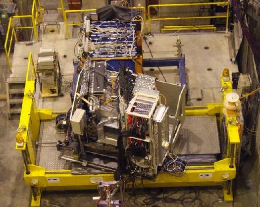
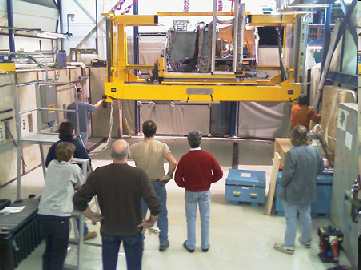
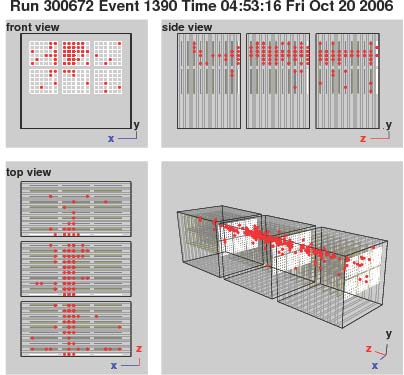
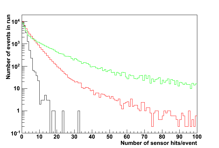
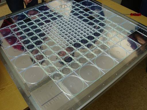
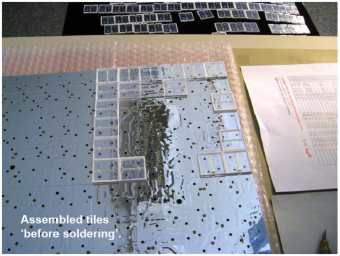
In the years 2008 and 2009 the CALICE collaboration successfully commissioned and operated four calorimeter prototypes in the MTBF beam-line at FNAL (Chicago). The detector chain consisting of the silicon-tungsten electromagnetic calorimeter (Si-W ECAL), the scintillator-iron analogue hadronic calorimeter (AHCAL) and the tail catcher and muon tracker (TCMT) had already been previously tested at the SPS (CERN) in the years 2006-07. The Si-W ECAL is a 30 layer sandwich structure with 1x1 cm2 cell segmentation. The AHCAL is a 38 layer structure with minimum cell size of 3x3 cm2. A new type of ECAL based on scintillator strips (4.51 cm2) and tungsten absorbers (Sc-W ECAL) replaced the Si-W ECAL during two test beam campaigns in September 2008 and May 2009. In total four campaigns were supported by CALICE at FNAL, each of about 6 weeks. Fig. 23 shows a step of the installation of the CALICE set-up at FNAL, next to a open active layer of the AHCAL prototype.
In addition to these combined campaigns, several smaller beam test runs were performed for individual detectors and the results from these are described in the relevant sections.
The detectors were commissioned making large use of the charge injection and LED monitoring systems. In all four campaigns the commissioning phase took no longer then one week. The equalization of the cells’ response was performed in situ using dedicated calibration runs using a 32 GeV muon beam. The physics program covered with both detector configurations included electron runs in the energy range 1–30 GeV, pions runs at 1–60 GeV, and proton runs in the range 10–60 GeV. Particular interest for the physics program was to cover the region 1–6 GeV not covered at the CERN SPS. In addition the Sc-W ECAL program included special runs, in which the were generated by firing a 16–32 GeV beam at an additional target on the beam-line, immediately in front of the detector.
Data were collected for both detector configurations under an incident beam angle of 90 degrees to the detector planes (default configuration, zero rotation) and in inclined positions of 80, 70 and 60 degrees, making use of the movable stage support hosting the ECAL and HCAL detectors. In addition, scans were performed to study uniformity of response as a function of the beam impact point on the detector surface.
A total of 87 million events were collected in the configuration including the Si-W ECAL, and 75 million events in the configuration including the Sc-W ECAL.
2.2 Si-W ECAL performance
A description of the SiW ECAL physics prototype follows in section 3. The Si-W ECAL was operated in the CERN beam tests in 2006-7, and in the first stage of the FNAL tests in 2008. It was exposed to beams of muons, electrons and hadrons. The muon data were used as the basis of detector calibration, so that recorded signals could be converted into minimum ionising particle (MIP) equivalents. The commissioning and calibration procedures have been described in some detail in [1].
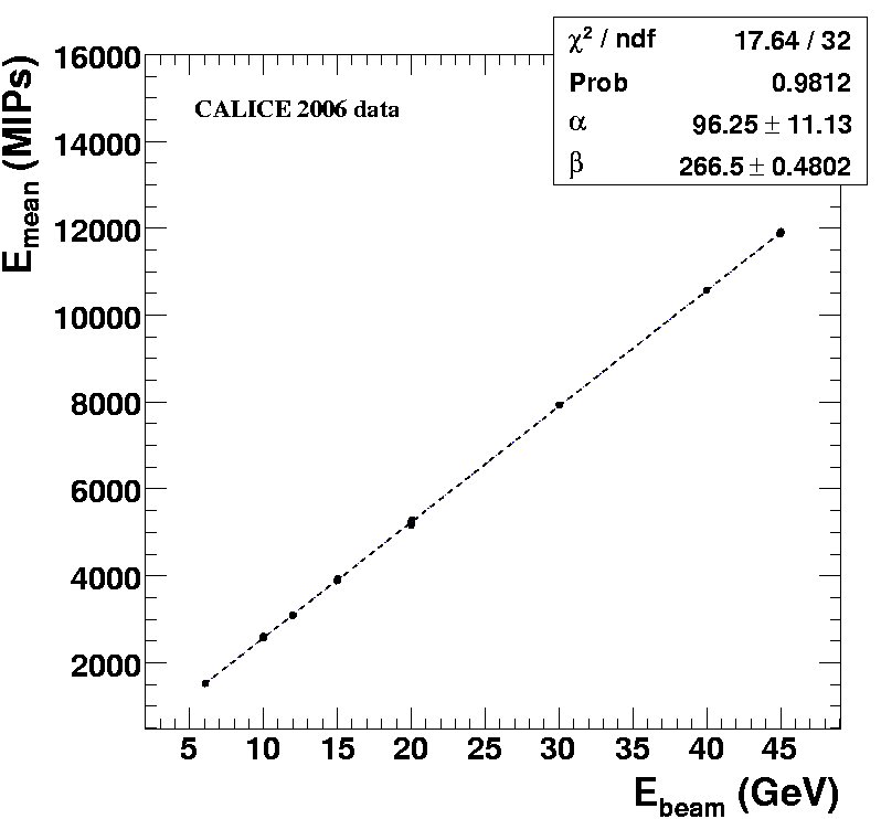
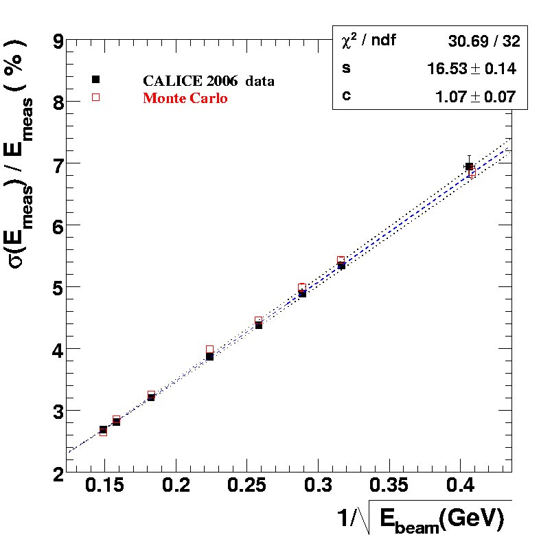
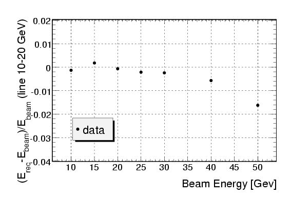
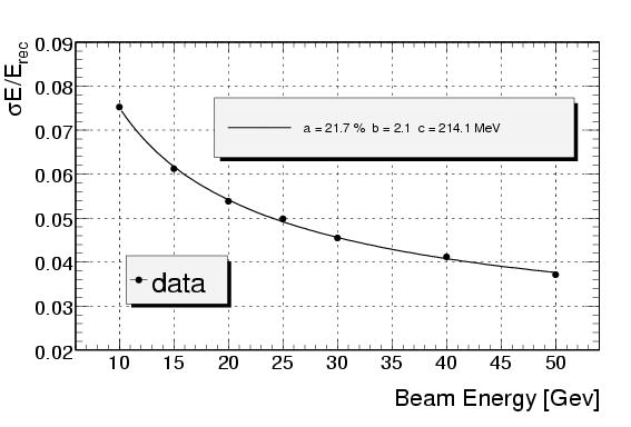
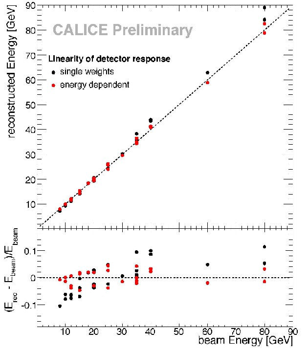
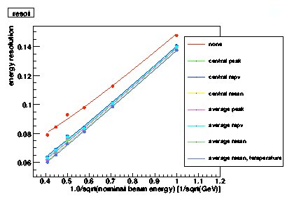
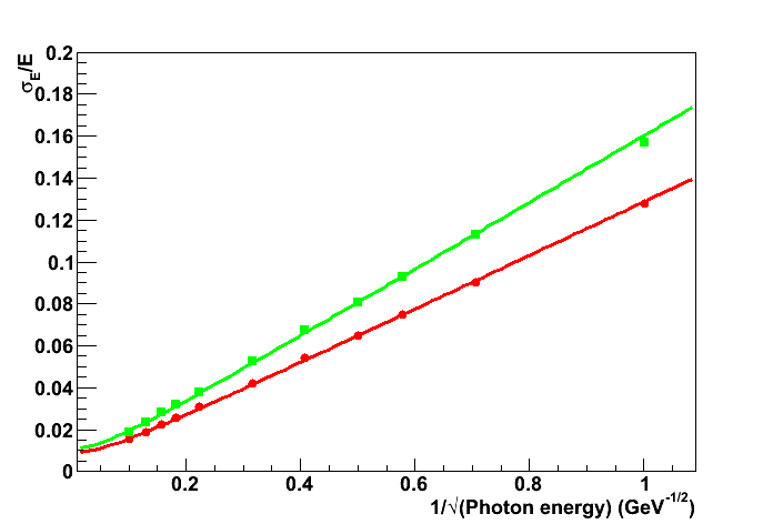
Some studies of the response of the ECAL to electron beams using the 2006 data have been published in [2]. Events are selected which lie well away from the edges of the test module and far from the inter-wafer gaps, in order to produce a clean sample for comparison with simulation. In Fig. 2 we show the measured response and energy resolution as a function of beam energy. The response is linear to better than 1%, though with a small offset from the origin, which is largely predicted by the simulation. The energy resolution is in agreement with that predicted for this configuration.
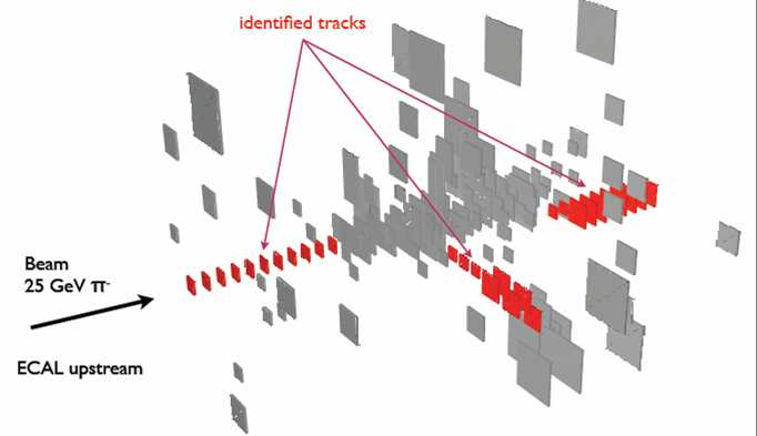
Many further studies using the ECAL data are in progress, for example tests of uniformity using a transverse scan of the detector in 2007, measurements of transverse and longitudinal shower profiles, and of position and angular resolution. Several of these have been presented in conference talks. Studies are also under way of the ECAL response to hadrons, which complement those using the HCAL. In particular, the high granularity and short radiation length of the ECAL permit interesting studies of the primary interaction in hadronic showers to be made (see Fig. 3).
2.3 AHCAL performance
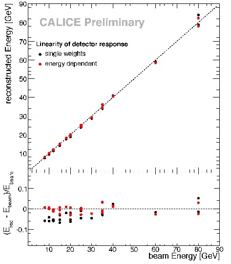
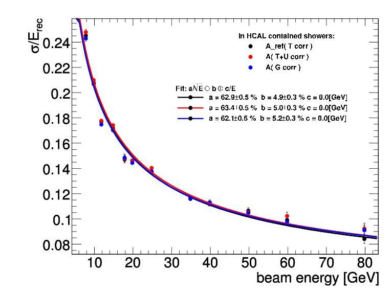
The completely instrumented AHCAL (described in section 6) was exposed to muon, electron and hadron beams in 2007-9, both with and without an ECAL in front. Muons were used for calibration. An important test of our understanding of the calorimeter is to check the response to electrons with no ECAL in front of the AHCAL. The energy density in electromagnetic showers is particularly large, so this is a good test of the important SiPM saturation corrections, and other effects [3]. In Fig. 4 we show the deviations from linearity of the electron response as a function of beam energy. Linearity better than 2% is obtained for electron energies up to 50 GeV. The energy resolution for electrons is also shown.
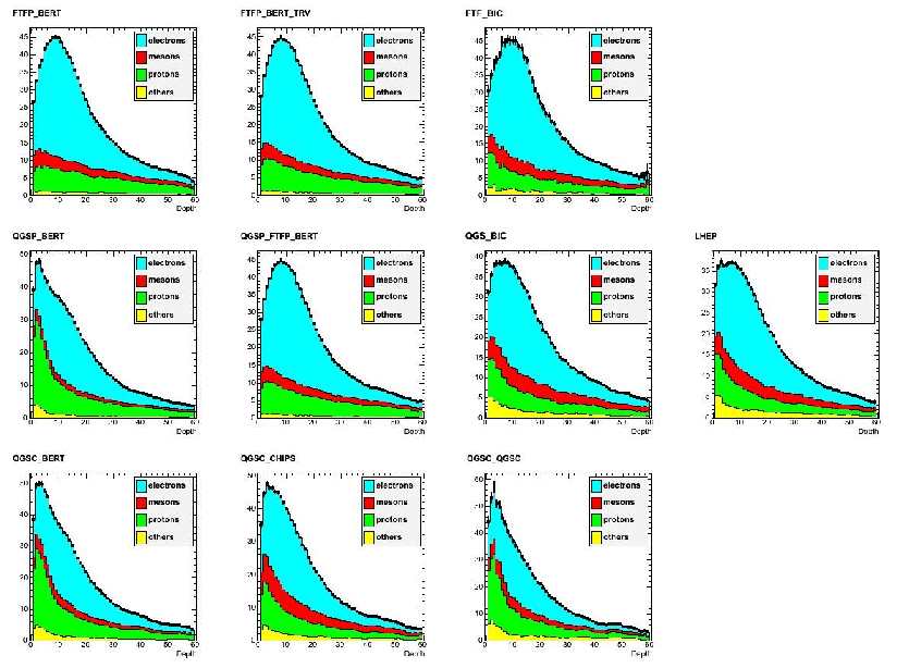
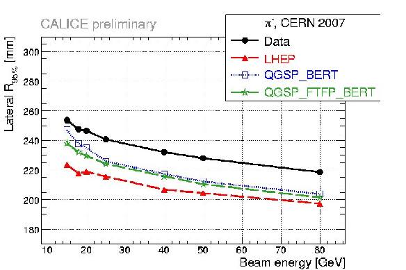
The transverse and longitudinal energy profiles of hadronic showers are important characteristics, which will be expected to influence the performance of particle flow algorithms. They can also be used to discriminate between Monte Carlo models. An example is shown in Fig. 5, which is based on measurements of the transverse shower profiles for pions, from which the mean shower radius and the radius for containment of 95% of the shower energy are extracted [4]. These are plotted against beam energy, and compared with the predictions of three of the many “physics lists” available in GEANT4. We note the need for caution in drawing hasty conclusions about the merits of different models - the model which describes one observable best may perform less well for a different variable, or at a different energy.

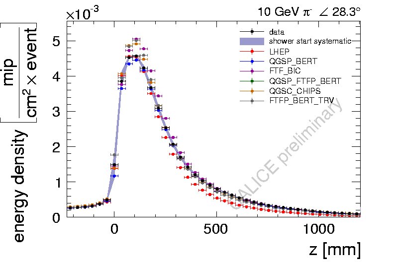
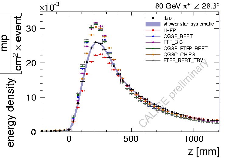
The longitudinal shower profile is important for particle flow, and can also be a useful discriminator between hadronic models. In order to make a sensitive measurement, it is helpful to deconvolve the distribution of shower starting points from the form of the subsequent shower development. We therefore developed an algorithm to identify the primary interaction point in the HCAL, and then measure the energy profile of the shower starting from this point. Typical distributions [5] are shown in Fig. 6, for pions of 10 and 80 GeV, and compared with a few GEANT4 physics lists. None of the simulations is perfect at all energies, and the LHEP model seems particularly unsuccessful. Work on studying the longitudinal shower development as a function of radius is also ongoing.
2.4 Combined performance
The CALICE calorimeters are non-compensating, i.e. they have different response to electrons and hadrons. However, because of their high granularity, it is often possible to identify the various components within a shower, and then weight them appropriately. One example of such “software compensation” is illustrated in Fig. 7. In this study, we exploited the fact that the electromagnetic components in a shower tend to have higher energy density. Accordingly, cells are given different weights depending on their energy. We optimized these weights (in a parameterised form) so as to optimise the energy resolution. As seen in Fig. 7 (taken from [6]), the energy resolution for single pions can be improved from over 60% to just below 50%. A potential danger of this approach is that it might affect the linearity of the response, but in fact we find the linearity is slightly improved as well. There is clearly scope for many future studies along these lines.
2.5 Sc-W ECAL performance
A small prototype of the scintillator-tungsten ECAL was tested in stand alone mode at DESY in 2007. This was followed by full-scale beam tests at FNAL in 2008 of a module of the same size as the Si-W prototype, with the AHCAL and TCMT behind. The scintillator was in the form of strips of size cm2, read out by MPPCs via wavelength-shifting fibers. Some of the first results of these beam tests [7] are shown in Fig. 8. At the present stage of understanding the data, the response to electrons is linear to better than 5%. An improved treatment of various corrections (temperature, for example) can be expected to improve this. The energy resolution is also shown, and is rather comparable to that of the Si-W ECAL.
3 Silicon-tungsten ECAL: Si-W ECAL
3.1 Physics prototype
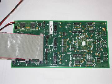
A small detector prototype, the “physics prototype”, was developed in order to study the physics performance of a sampling electromagnetic calorimeter suitable for use in detector at a future Linear Collider. The detector was designed to satisfy the requirements of the Particle Flow approach to event reconstruction, in particular a compact size, small Molière radius, and high granularity. A 30–layer sampling calorimeter design was chosen, with three different sampling fractions, finest in the first layers and coarser in the latter layers. Tungsten was used as absorber material due to its small Molière radius and large interaction to radiation length () ratio. The active layers were made of 525 thick silicon sensors, segmented into cells of cm2, giving the high granularity required for the particle flow approach.
These silicon detectors were mounted on printed circuit boards which channelled the signals to the front-end readout chip, mounted on the same PCB outside the detector volume. Two PCBs were mounted on each side of an “H”-shaped detector slab which also incorporated a layer of tungsten. These detector slabs were then inserted into an alveolar supporting structure composed of a carbon fiber-epoxy composite material, also incorporating the other half of the tungsten absorber layers.
3.2 Operational experience with physics prototype
This ECAL prototype was exposed to test beams in 2006-07 (at CERN) and 2008 (at FNAL). Several hundred million events were collected in total, comprising a mixture of calibration events and beam events with different particle species and momenta. Beams of electrons, positrons, muons, pions and protons were used at a range of momenta between 1 and 180 GeV/c. The detector ran stably over this three year operation period, in terms of calibration, energy response and linearity. No adverse ageing effects were observed.
In the next generation ECAL prototype (see below) the front end electronics will be placed inside the detector volume. A concern is that the electronics chips might produce spurious signals when they lie in the centre of a dense electromagnetic shower. To test this, a special detector slab was prepared, consisting of four readout chips, without any silicon wafers. This layer was placed into the physics prototype structure at the depth of the electromagnetic shower maximum, and exposed to high energy electrons. An analysis of the resulting data has shown that there are no effects of fake signals due to this effect.
3.3 Physics prototype detector performance
The electron data collected have been used to measure the detector performance, as described in Sec. 2.2.
Several inconvenient features were encountered in the operation of the detector. Some chips showed unstable pedestal values during the running period, requiring offline corrections to be applied to the data. This feature was understood, and will be remedied in future designs.
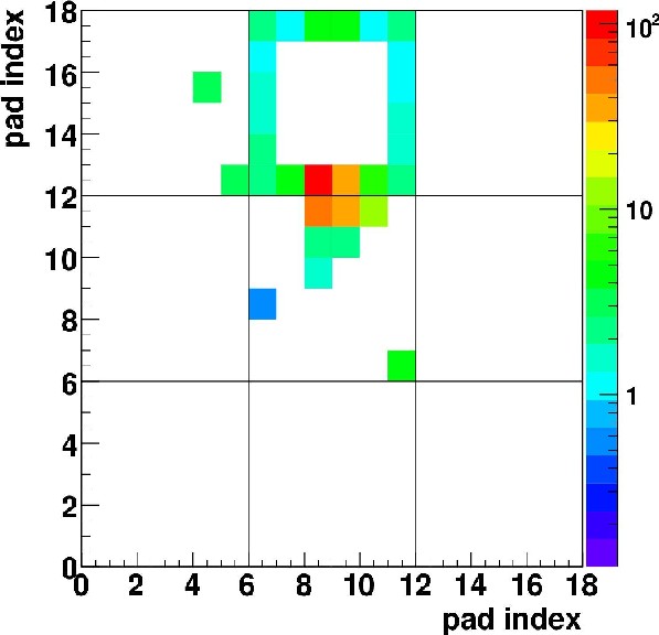
An interesting problem was observed when an electron deposited energy in the guard ring (a structure at the edge of the silicon sensor which protects against high voltage breakdown). The deposited charge propagates around this structure, which, via the coupling between the guard ring and adjacent cells, produced events containing distinctive square shapes, with signals seen in all the cells at the sensor edge (see Fig. 10). This feature of the sensor has prompted R&D to improve its design.
3.4 Conceptual issues for the technical prototype
The next stage towards the realisation of a final detector for a Linear Collider detector is the production of a technical prototype. This is conceived as a slightly smaller scale version of a single module of the final ECAL detector. It has the same shape as the ILD ECAL module design, the same number of layers, but somewhat smaller transverse dimensions (see Fig. 11).
This next generation of silicon detectors will have a granularity four times higher than in the physics prototype, with a cell size of mm2. To minimise the effect of dead areas at the edge of silicon sensors, larger cm2 sensors have been developed. The design of the sensors’ guard rings is under investigation to minimise the propagation of signals along the ring and the appearance of the so-called “square events”, mentioned above.
In contrast to the physics prototype, where the front end electronics was placed outside the detector volume, the technical prototype will have the electronics directly embedded in the PCBs which support the silicon detectors. This requires the design of ambitiously thin and complex PCBs, and studies of the bonding and encapsulation of unpackaged chips.
The front end chip must consume very little power to prevent massive cooling requirements. They should in particular make use of the ILC bunch structure, where beam is delivered to the detectors only of the time. A power-pulsed design of the electronics will allow the chips to be powered for only the time when beam is delivered (plus some readout time), and will be powered down for the remaining of the time.
The zero-suppressed, digitised signals from the front-end electronics are then passed to the common CALICE DAQ system (see Sec. 10).
3.5 Status and plans for the technical prototype
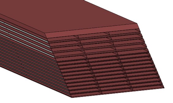
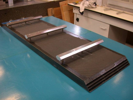
To study the fabrication of the tungsten-composite mechanical alveolar structure, an intermediate step, a three-layer “demonstrator” module has been constructed (Fig. 12). This allowed the study of composite layer manufacture, cutting and finishing, as well as the assembly of the various layers into a final structure, together with tungsten plates and the thick composite back- and front-plates which provide the rigidity of the module. The manufacture of this module was a success, and the measured dimensions of the module satisfy the mechanical requirements. The ECAL will be fixed to the inner surface of the HCAL via a system of rails on the outer face of the ECAL modules. The demonstrator module incorporated such rails.
Work has recently started on the manufacture of the larger alveolar layers for the technical prototype. A first layer has been constructed using new moulds to reflect the larger size of the detector slabs for this prototype.
Research and development of the silicon sensors is in progress. Forty cm2 wafers with mm2 pixels have been supplied by Hamamatsu. A number of these sensors have been tested and show satisfactory performance. An ongoing collaboration together with OnSemi and the Institute of Physics (Prague) is studying the design of the guard rings to minimise the occurrence of “square events”. A number of small test sensors have been produced with different guard ring structures. Tests show that these designs do indeed reduce the propagation of signals around the wafer edge.
In the medium term, links will be forged with further industrial partners. This will introduce an element of competition to the sensor production, which should help to reduce the sensor cost, which is at present uncomfortably high when a complete ILC detector ECAL is considered. The EUDET ECAL module will be instrumented with sensors from a number of different producers.
The construction of the detector slabs is under study. A long string of up to 10 Active Sensor Units (ASU, the PCB supporting the silicon detectors) must be connected together. This connection is both mechanical and electrical - to supply power and send and receive data to the front-end chips. There are strong constraints on the available space for these connections, so a very thin, mechanically and electrically robust system is under design. A dedicated assembly bench has been produced, which allows safe and well controlled manipulation of the delicate ASU elements. Studies of ASU connection are underway.
The front-end chips are being designed. The EUDET module will be equipped with SKIROC2 chips, see Sec. 9. Since these are not yet available, in the meantime tests will be carried out using the SPIROC2 chip. This chip can be operated in a “SKIROC mode”, in which its behavior is rather close to that envisaged for the SKIROC2 chip; however it has a smaller number of channels than the SKIROC2 chip, allowing only a subset of silicon cells to be read out. The operation of this chip in SKIROC mode has been tested on an electronics test-bench, and shows the expected characteristics.
The design of the PCB is under study. The PCBs for the technical prototype will, in contrast to the PCBs used in the previous prototype, will hold the front-end chips inside the detector volume. The space available for the PCB is limited, to avoid degrading the detector performance; it must have a height of not larger than 1.2mm. This constraint places particular emphasis on the integration of the chips onto the PCBs and on how they are bonded. A functional version of the board with relaxed requirements on the thickness has been manufactured, and is being tested. Further prototypes are being designed and submitted to manufacturers.
A cosmic test-bench is under preparation, which will allow the whole chain of sensors, PCB, front-end electronics and DAQ system to be tested and debugged.
The removal of heat produced in the front-end electronics from the detector structure is essential for the integration of the ECAL into the general detector. At present a 500 m sheet of copper extends along the length of the detector slab, acting as a thermal drain. The heat is extracted from this copper drain at the end of each module by a water-cooled system. Several possible designs for this system are under consideration, and a number of prototypes have been built.
We plan to instrument a cm2 tower of the next prototype (consisting of 30 layers) with sensors. One long detector slab will be prepared, to allow the testing of signal propagation along the entire 1.5 m length of a detector slab. The remainder will be composed of short detector slabs, each holding silicon sensors per layer. The detector will be gradually instrumented as silicon wafers become available. A series of cosmic and beam tests will allow tests of the whole detector system, even with a partial complement of silicon elements. Combined tests with other detectors (HCAL, tracking, muon) are foreseen as part of the CALICE program.
4 Scintillator-tungsten ECAL: Sc-W ECAL
The scintillator ECAL group which consists of 4 universities from Asia, Kobe, Kyungpook, Shinshu and Tskububa, is developing an EM calorimeter with tungsten absorber and scintillator strips according to the idea of PFA. In order to satisfy the requirements of PFA, the ECAL is expected to have fine segmentation of the order of a cm. To achieve this with scintillator we arrange plastic scintillator strips with 1cm width orthogonally in successive layers. A strip is read out by a small silicon photo-sensor called MPPC via a wavelength shifting fiber inserted in a hole in the scintillator strip.
An example of integration of the system as a calorimeter, we produced a small prototype which was tested at the DESY test beam in 2007. Then we have constructed a four-times bigger physics prototype and tested it at FNAL in years ’08-’09.
4.1 Operational experience with the physics prototype
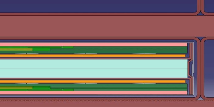
We have constructed a 26 layer Sci-W ECAL with 18 strips/layer. The detector has a sandwich structure of 3.5 mm tungsten and 3 mm scintillator. The absorber layer is composed of 88% tungsten, 12% cobalt and about 0.5% carbon, and has Moliere radius of 10 mm. The scintillator layer has 92 scintillator strips of size 4.51 cm2. In successive scintillator layers, the strips are alternately aligned vertically (X layers) and horizontally (Y layers). The scintillation light is read out by MPPCs (produced by Hamamatsu Photonics Co.). The MPPC is one of the novel pixelated Geiger Mode Avalanche photo diode, such as SiPM. A MPPC consists of a matrix of micro APD pixels of 25 . The total number of pixels in a device is 4040=1600 pixels in 1 mm2. The structure of the Sci-W ECAL test module is shown in Figure 13.
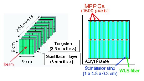
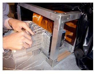
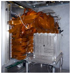
The MPPCs are mounted in a hole in the end of each scintillator strip and soldered to a flat cable. Signals from the MPPCs are fed into the AHCAL baseboard through the flat cable. Figure 14 shows a photograph of the Sci-W ECAL test module mounted in the beam line. The size of the entire module is about 9920 cm3 and the total number of readout channels is 468.
The module was tested at DESY with positrons at energies between 1 and 6 GeV. We use a combination of trigger and veto counters to trigger events. The trigger counters consist of a 331 cm scintillator block read out by two photo-multipliers. Two trigger counters and one veto counter were installed in the beamline upstream of the ECAL module and used to select 1 MIP events. One veto counter was located downstream of the ECAL and used to select positrons which do not shower during their passage through the ECAL when active layers were exposed outside the absorber structure. Such MIP events are used to calibrate the detector response.
Each strip was calibrated by these MIP events. Four layers of drift chambers were placed in the beamline to perform precise particle tracking. Each drift chamber layer has both x and y wires. The ECAL test module was mounted on a movable stage, allowing it to be moved with 0.1 mm accuracy in the plane transverse to the beamline.
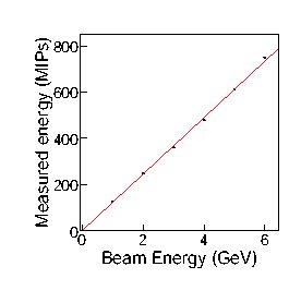
The energy response of the calorimeter is shown in figure 15 (left) which indicates good linearity. The resolution is also derived from these measurements as shown in Figure 15 (right). The structure of the Sci-W ECAL test module is shown in Figure 13.
The red dots and red line are corresponding to the extruded scintillator which was introduced at the first time for this test. The difference is expected from a simulation to be due to the non-uniformity of strips along the wave length shifting fiber , which is measured as shown in figure 16.
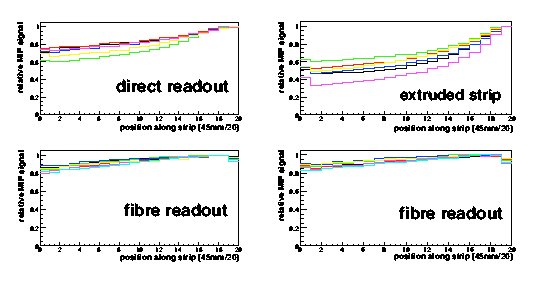
In this test beam experiment we have employed three different types of scintillator from two different manufactures. The direct and fiber readout scintillator are made by Kuraray, and the extruded strips are produced by Misung CO. in Korea. The non-uniformity is clearly larger for extruded ones. Since the cost of the scintillator for the extruded is quite low, we decided to improve the performance for the extruded in Korea for the next beam test at FNAL.
Subsequently, we have built the Sci-W ECAL with MPPC and extruded scintillator with 4 times bigger volume, which is shown in figure 17.
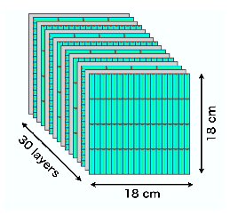
The second Sci-W ECAL prototype incorporates the improvements suggested by the results of the first test beam experience, although keeping the readout scheme and electronics. It is 1818 cm2 in lateral size and composed of 30 layers. The number of radiation lengths of this calorimeter is 21 X0, although the same tungsten plates were employed. A scintillator layer consists of 4 x 18 =72 strips of 14.5 cm2 with 3 mm thickness. Even layers have X-strip and odd layers have Y-strips with WLSF read out covered by a good reflector film of KIMOTO CO.. This prototype has been tested during two comprehensive beam test periods at FNAL, in Sep. 2008 and May 2009. The prototype was operated together with the AHCAL and the TCMT to evaluate the combined performance of calorimeters within the framework of CALICE. Electron and charged pion beams with an energy between 1 GeV and 32 GeV were used. Beams were injected into the central region and uniform region, to confirm the improvement in uniformity of scintillator response. The detector was calibrated using a 32 GeV muon beam.
Using muons as minimum ionizing particles the MIP calibration constants for 2160 channels is 160 ADC counts. It is a factor 10 larger than the corresponding standard deviation of the pedestal which is 15 ADC counts. The statistic uncertainty of the MIP response on each channel is less than 0.6% even in the worst channels. There are five dead channels due to broken photo-sensors or too high levels of background noise. The contribution of the dead channels to the energy measurement is negligible.
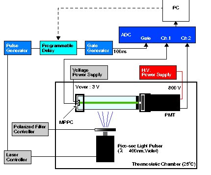
The MPPC response has a saturation behavior according to its intrinsic property. Thus a saturation correction for each MPPC must be implemented. We have measured the saturation effect of the MPPC using a simple bench test in advance to perform the beam test. Figure 18 shows the setup of the response curve measurement using pico-second laser system, the scintillator-strip and the MPPC.
The measured MPPC response function is modeled with the function, , where is the number of photons detected by the MPPC, is the total number of pixels on the MPPC, e is the photon detection efficiency and is the number of photons incident in the MPPC sensitive area. From the fit to the curve in Figure 18, one finds . The actual number of pixels in the MPPC device is 1600. The higher value found for is due to the fact that photon generation in the scintillator has a time duration which allows some pixels to recover and fire a second time. After applying saturation correction according to our own measurements the linearity of the electron energy response in the range 1-32 GeV is better than 1%.
4.2 Further plans for R&D and integration
The results obtained during the three beam test campaigns and with
test bench studies indicate that the Sci-W ECAL fulfills the requirements
for a particle flow detector.
However, further improvements are expected
by introducing MPPC with more pixels, and scintillators with smaller strip
width.
Our further R&D for the coming years (2010-2012) will cover the following points:
(1) software effort: integrate Sci-W ECAL in the reconstruction and analysis framework of CALICE.
(2) integrate of electronics inside the sandwich layer structure,
(3) increase the scintillator segmentation to 5 mm wide strips,
(4) increase the number of pixel in the MPPC.
5 Digital ECAL: DECAL
5.1 Concept
Studies based on the concept of a digital ECAL (DECAL) started in 2006. The groups involved so far have all been based in the UK and, due to the serious funding difficulties for ILC work there, the project has been limited in effort. Since 2008, the groups involved in the DECAL work are also members of the UK SPiDeR collaboration, as the sensor implementation is likely to use Monolithic Active Pixel Sensors (MAPS) in CMOS. Hence, the technological aspects of the sensor design are covered in the SPiDeR submission to this PRC meeting [13].
The basic idea of a DECAL is to use very fine granularity silicon sensors with binary pixel readout for the active layers of a silicon-tungsten ECAL, so as to make an estimate of the number of charged particles in each layer. These sensors would be used in place of the analogue ECAL silicon wafers but otherwise the aim is that other aspects of the ECAL design, such as the mechanics, would be unchanged. This would allow the DECAL to be a “swap-in” option for a silicon-tungsten ECAL. Note, it also means such a sensor would need to have a similar power consumption to the analogue ECAL.
In order to count charged particles with binary readout, then the pixel size must be much smaller than the separation of particles within the showers so that the probability of two particles hitting the same pixel is kept small. According to simulations, the density of charged particles in the innermost core of the highest energy electromagnetic showers expected for a LC may have a tail reaching to around 100 mm-2. However, high energy electromagnetic showers have not been measured accurately at a high level of granularity. Knowledge of the actual shower density is clearly critical for the optimisation of the pixel size and this is one of the major initial aims of the DECAL work. For the studies performed so far, a pixel size of m2 has been assumed. This would require an ECAL for a LC detector to have pixels.
5.2 Motivation
One basic motivation for a DECAL is that there is potentially a significant improvement in the electromagnetic shower resolution. ECALs usually work on the principle that the number of charged particles passing through each layer is on average proportional to the incident particle energy; there are fluctuations around this average due to the stochastic nature of the shower development. These charged particles lose energy in traversing the sensitive layers of the ECAL and the energy loss per particle also has fluctuations, mainly due to the Landau distribution of energy deposited but also due to variations in their speed and path length through the material. An analogue ECAL therefore has contributions to the energy resolution both from the intrinsic shower fluctuations and also from the variations of the energy per charged particle. The basic idea of a DECAL would be to reduce (or eliminate) the latter contribution by attempting to measure the number of charged particles directly. Figure 19 shows an example of the fundamental resolution of electromagnetic showers simulated with an analogue and a digital calorimeter of the same geometry. In this example, the ECAL had 20 layers of tungsten of thickness followed by 10 layers of thickness for a total of ; these are typical of LC designs. In both cases, the resolutions shown are “ideal”, meaning they are based on perfect information with no dead regions, electronics noise, threshold suppression etc. It is thought that a realistic analogue ECAL will approach this idealised value and the purpose of the DECAL studies is to determine the degree to which this is true for the digital case. Simulation studies so far indicate a degradation in the stochastic term from 0.128 to around 0.14; this is still better than the ideal analogue case. A major uncertainty in this more realistic resolution is the core shower density, as mentioned above; hence the need to measure this directly.
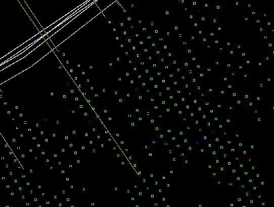
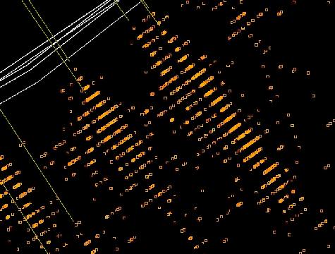
The LC detector calorimeter designs are mainly driven by PFA performance, rather than electromagnetic resolution; the latter plays only a small role in the jet energy resolution which is more significantly affected by the “confusion term” due to mis-association of charged tracks and calorimeter deposits. Systematic studies of the effect of having a very highly granular DECAL rather than an analogue ECAL on the PFA performance have not yet been done. However, figure 20 shows visually the difference of the two in a simulated ILC hadronic jet. It seems clear the much improved position resolution (from around 5 mm to 50 m) should not degrade the PFA performance and can only help in untangling the detailed jet structure.
A further motivation for these studies is the ECAL cost. A silicon-tungsten ECAL for a LC detector is likely to require around 2000 m2 of silicon wafers in total. The cost of these silicon wafers is of course an extremely important factor. The analogue ECAL requires high resistivity wafers which are not otherwise very widely used. This limits the number of vendors who will fabricate such wafers. In contrast, the aim is to make DECAL sensors using very standard CMOS processes which are widely available. Having a large number of vendors for the sensor production should help keep the price as low as possible.
5.3 The TPAC beam test at CERN
The TPAC sensor was fabricated to study the issues of a DECAL sensor for a LC detector. A stack of six layers with one TPAC sensor per layer was operated at CERN in August this year mainly for detailed performance measurements with MIPs. Figure 21 shows the equipment at the beam area. Details of the TPAC sensor and the results from these MIP measurements are discussed in the SPiDeR submission [13].
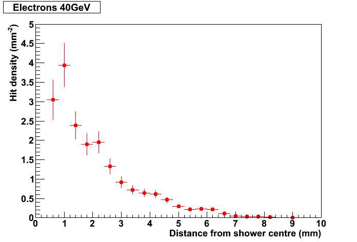
This sensor was not intended for full shower reconstruction as it has an active area of only mm2, smaller than the Molière radius of tungsten. Hence running with electron beams was not an intended goal of this beam test, particularly as the TPAC stack was running parasitically to other main users who did not require electrons. However, an unexpected opportunity for one day arose and the stack was exposed to electron beams. For these runs, a 30 mm stack of tungsten was added in front of the first sensor layer. This corresponds to of material, meaning the particles emerge at close to shower maximum. There was no further tungsten between the six sensor layers. These data allow a first look at the core densities of electromagnetic showers. Figure 22 shows the much larger number of hits seen in time with the trigger for the electron data than with pions.
The shower centre was reconstructed by taking the average position of all pixel hits in time with the trigger in the last five layers. By comparing the centre found using various combinations of layers, the resolution on the shower centre using the five layers was found to be around 0.8 mm. The shower centre was extrapolated to the first sensor layer and the density of hits in this layer relative to the reconstructed centre was found. Figure 22 also shows the average density distribution for electron showers. Note, the dense core of the shower is averaged out to some extent by the resolution of the shower centre and the tail is truncated by the size of the sensor.
5.4 Future plans
In the short term, it is critical to make further measurements of the core shower density. It is clear external tracking would help locate the shower centre much more accurately and so a further beam test early in 2010 is planned at the electron beams at DESY where the EUDET telescope will be available. The DESY electron beams are limited to 6 GeV so another beam test at CERN may be undertaken, if a slot is granted, later in 2010.
Longer term, a larger sensor will be produced to do a “physics prototype” measurement of electromagnetic showers in a full-depth DECAL stack. The development of this sensor is part of the SPiDeR program and the technical aspects are discussed in that submission [13]. The schedule is to produce a 30 layer DECAL stack in 2012 and expose it to beam in a lengthy campaign that year, of equivalent scope to that of the analogue ECAL in 2006/7.
The main aim of this program is a proof-of-principle of a DECAL. These measurements should also give valuable physics information on electromagnetic showers, useful for tuning simulations. In addition, the data will give critical information required for the optimisation of a real LC detector digital ECAL sensor in the future. Specifically, the pixel size is a critical factor; if the DECAL sensor measurements show the pixel size can be relaxed to e.g. m2, then the power consumption would be directly reduced by a factor of four. The effect of noise on the resolution should also be understood so slowing the pixel response (to again save power) may then be an option if integrating over a few bunch crossings can be shown not to degrade the performance. Another issue is that the on-sensor memory storage causes dead area so the importance of reducing this, potentially using smaller feature size processes, compared with the risk of filling memory and hence losing hits, will be clearer.
6 Analogue HCAL: AHCAL
6.1 Performance of the physics prototype and operational experience
The analog hadron calorimeter prototype (AHCAL) consists of a 38-layer sandwich structure of steel plates (4.5 and fine-segmented scintillator tiles ( cm2 in the core region) that are read out by wavelength-shifting fibers coupled to SiPMs. There are 7608 channels in total.
The signal is amplified and shaped using a modified version of the ASIC of the Si-W ECAL prototype. A calibration/monitoring system based on LED light monitors the SIPM gain and can measure the full SiPM response curves in order to cross-check the non-linearity corrections derived from test bench data.
The prototype has been operated for four consecutive years at two different test beam sites. The bias voltage of the detector is adjusted to set nominal light yield to 15 pixels/MIP for all channels. The average noise level per cell during the different test beam campaigns has been around (1.3-2) 10-3 as expected from the test bench, but about a factor 10 higher than the final design goal. This is the first time that such a large quantity of SiPMs is operated over longer periods. The detector had an initial number of dead channels corresponding to 2% of the total. An additional 0.5% of channels died during transportation to FNAL. The large majority of these are due to bad soldering or subsequent broken connection. A detailed study of SiPM performance over two years of operation (’07-’08) reveals that this number has been very stable during operation. Only 5 SiPMs died during operation, possibly due to too high current induced by surface defects. The SiPM used in the CALICE AHCAL thus demonstrated excellent stability during four months of operation.
6.2 Calibration and stability
The calibration scheme for the conceived scintillator HCAL is based on test bench characterizations and test beam data. While electromagnetic, hadronic and weighted energy scales can be established with sample structures of the HCAL alone or in conjunction with the ECAL exposed to beams of muons, electrons and hadrons, the equalization of the detector cells must be established with muon beams for all active layers of the detector individually. Due to the proposed deep underground site, the power pulsed electronics and the fine segmentation, cell equalization cannot be repeated using cosmic rays.
The calibration accuracy is maintained using LED monitoring of the photo-sensor gain, in-situ MIP calibration based on track segments in hadron showers and classical slow-control recording of the relevant operation parameters, temperature and bias voltage. These methods have been successfully applied to test beam data.
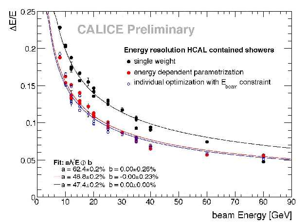
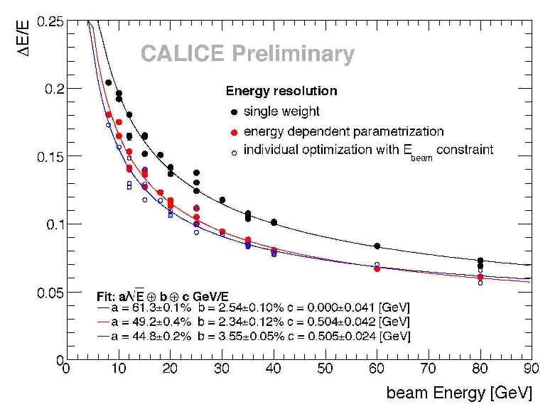
Simulating ILC events and using algorithms bench-marked with test beam data, we have quantitatively determined the required luminosity for in-situ MIP calibration of individual cells and of average values for sub-sections of the detector. A cell-by-cell MIP calibration is not possible with realistic running times, but it is also not necessary. Using fully detailed simulations of the ILD detector and reconstruction based on the Pandora particle flow algorithm [8], we have modeled different scenarios of statistically independent as well as coherent mis-calibration effects, affecting the entire HCAL or parts of it. Purely statistical variations, like those arising from calibration errors or random aging effects, hardly affect the hadron energy resolution at all, due to the large number of individual cells contributing (10 per GeV). Coherent effects which could for example arise from uncorrected temperature variation induced changes of the response are potentially more harmful if they affect a large portion of the detector. However, these are also easy to detect, and propagate only mildly into the jet energy resolution.
We have demonstrated the validity of these simulation based [10] estimates by treating our test beam experiment like a collider detector, using cell-by-cell inter-calibrations only from data taking at a different site, under different conditions and after having it exposed to disassembly, transport and re-assembly influences. Applying only in-situ monitoring techniques, we re-established the scale and reproduced the resolution; see the right plot in Fig. 24. The constant term is larger here than reported in the analysis section due to a preliminary set of calibration constants used. Imperfections, due to intermittent hardware malfunction, and absent in any simulation showed up, but were successfully compensated.
This is an important outcome of the test beam runs at CERN and at FNAL; it gives confidence that the high granularity approach with the novel SiPM technology can be extrapolated to the full detector scale.
6.3 Development of a technological prototype
In order to validate the concept of a highly granular scintillator based HCAL, it needs to be demonstrated that the high channel density can actually be realized without compromising the performance by too many dead spaces or reduced compactness and hermeticity once readout and calibration electronics or support structures have been accommodated. In this respect the physics prototype is not scalable and needs to be complemented by a technological prototypes addressing these integration issues.
The envisaged detector architecture [9] is sketched in Fig. 25. It is inspired by one variant of the ILD detector concept, but is very similar to those envisaged for SiD or CLIC. The Figure shows one sector of a barrel subdivided only once along the beam axis. This layout provides access to electronics and service interfaces once the detector end-cap is opened, but poses tight space constraints to the barrel end-cap transition region.
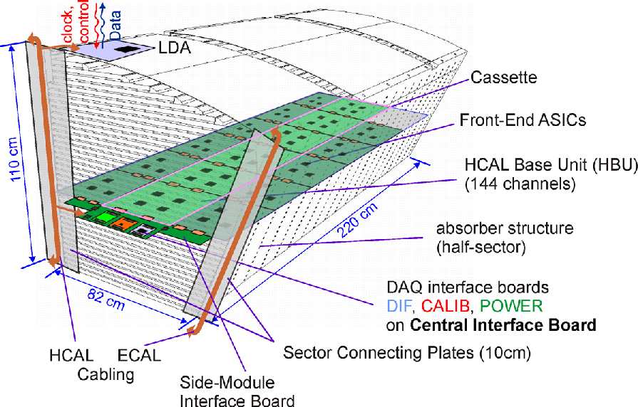
Compared with existing hadron calorimeters, the particle flow HCAL has a rather fine longitudinal sampling, with a correspondingly high pressure on the thickness of the active layer gaps, but also on mechanical tolerances. This, together with the requirement of minimum dead zones represents an engineering challenge which is being addressed now.
There are 48 independent read-out layers which must be as thin as possible in order to keep the overall detector volume small, as it has to fit inside the main solenoid of the collider detector and still provide maximum hadronic absorption depth. Each layer has a fine transverse segmentation, again with individual cell read-out, which requires concentrating the data at an early stage in order to keep connectivity issues manageable and reduce dead areas occupied by external electronics components.
The readout ASICs process the signals including digitization and intermediate storage. Thanks to their operation with pulsed power synchronous with the accelerator time structure, no cooling inside the modules is necessary. Only interfaces to DAQ, power supplies and calibration control are placed outside the volume.
We foresee a staged prototype program to validate this concept:
-
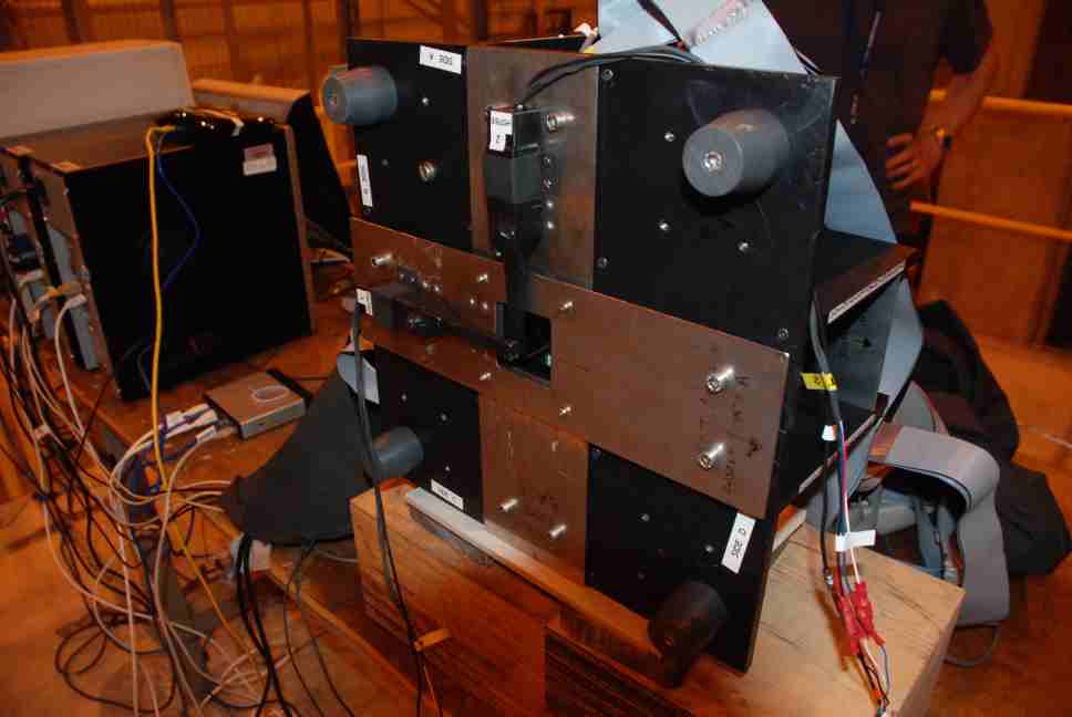
1.
A horizontal test structure (Fig. 26 right) to establish the mechanical tolerances and electronics signal integrity over the full area and length of the module. Heat dissipation and installation procedures can also be studied in full scale.
-
2.
A vertical test structure (Fig. 26 left) to establish the mechanical stability under various orientation and stresses as well as multi-layer electronics integration and operation. This can be tested with electron beams and requires instrumentation of a small volume only.
-
3.
The vertical structures can be stacked in a flexible way, according to the needed overall test beam geometry, and their instrumentation completed for hadron shower studies.
The first two steps can be accomplished with about one to two thousand channels, the third will require about 40’000 channels. The multi-layer set-ups need a compact realization of the interface electronics components.
In addition to the demonstration, that the mechanical and electronics design challenges can be met, there are operational and physics issues to be studied, which could not be tackled with the physics prototype:
-
•
Establish stable operation with auto-triggering and on-detector zero-suppression. This will require continuous monitoring of thresholds and in-time adjustment of bias voltages to compensate for temperature induced variations of the signal.
-
•
The new ASICs incorporate a TDC for a time measurement of calorimeter hits. It must be shown that this system can be timed in and operated stably.
-
•
The usefulness of the timing measurement for neutron hit identification and shower reconstruction can be evaluated.
-
•
The time evolution of hadron showers in simulation models can be confronted with experimental data; for the first time in a spatially resolved way.
-
•
The stainless steel structure allows for operation of the calorimeter in a magnetic field, and to test the predicted influence of the field on hadron shower propagation.
6.4 Mechanical structures
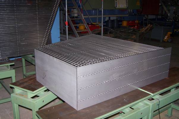
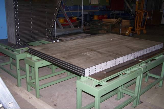
The module consists of stainless steel plates with 16 mm thickness which are supported only by the 5mm thick side panels, without additional spacers. The gaps can be filled completely with active elements.
The mechanical stability of this ambitious design has been extensively studied using finite element methods. Deformations of the individual module as well as the overall barrel structure were validated, taking external support and the suspension of the ECAL into account.
It is straightforward to keep the required tolerances by precisely machining all absorber plate surfaces. However, the cost would be higher by a factor 2 to 3 with respect to the raw material. Since cost optimization is an important ingredient in a ”realistic” structure, we aim at producing the structures from raw, commercially available rolled plates. In particular the flatness of the plates, as specified by commercial standards, exceeds the requirements by intolerable amounts. We have prepared devices for measuring deviations and found a cost-effective solution (roller leveling) to achieve the required flatness within a millimeter across the full module.
The horizontal and two vertical test structures are shown in Fig. LABEL:fig:ahcalstacks. The first has 4 plates, 2160 mm long, the second is 360 mm deep.
6.5 Readout and calibration electronics
The electronics is subdivided into HCAL Base Units (HBUs) in order to keep the single modules at reasonable sizes concerning production and handling. The HBU with a typical size of cm2 integrates 144 scintillating tiles each with Multi-Pixel Geiger-Mode Photo-diodes (MGPDs). The analogue signals of the MGPDs are read out by four front-end ASICs (SPIROC, [3]). The full depth of a sector is covered by 6 HBUs that are connected together by so called interconnection flexleads. A chain of 6 HBUs forms an electrical layer unit. the so called slab. At the end of the sector, the electronics of a detector layer are connected to the detector interface module DIF and the AHCAL specific modules for calibration (CALIB) and the power-supply module (POWER).
In order to keep the development time for the first prototype modules as short as possible, the first DIF module is realized by a commercial FPGA board. The modules CALIB and POWER are realized as mezzanine modules on top of the DIF, while the interface to the first HBU prototype is realized by the final thin flexlead interconnections via the CALIB module. The prototype setup shown in Fig. 27 can be used to test all electrical characteristics of a full layer in the horizontal test structure.
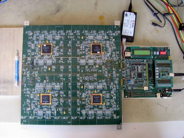
The electronic commissioning has been completed using LED signals, and the first HBU prototype will be exposed to the DESY test beam in November. The DIF board will be read out via USB; the final DAQ chain will be commissioned in 2010, this can start with the FPGA board. There are still two SPIROC chips of the first version of the HBU, which have a thicker package, therefore a re-design of the board layout will be needed for the full layer test.
The AHCAL specific module CALIB is used to control and operate the light calibration system that is based on electrical signal distribution (see below) as well as a charge -injection system that can be used for calibration and debugging as well. The POWER module provides the supply voltages for the inner-detector electronics as well as for the modules DIF and CALIB, and the MGPD bias voltage. The architecture of the power regulator setup has been defined in detailed measurements of the power-pulsing characteristics. A settling time below 10 s can be expected.
For the LED calibration and monitoring system we follow two approaches, one based on a central driver and optical signal distribution, one based on electrical signal distribution and an individual LED per tile. The latter is already integrated in the HBU, but not yet fully optimized. The aim is to equalize the light intensity and maximize its dynamic range. The former distributes light by a notched fibre to a row of tiles.
6.6 Scintillator and photo-sensor development
Following the successful operation of the physics prototype, progress was made by various manufacturers, e.g. in Russia or Japan, to provide sensors with lower dark count rate and / or smaller inter-pixel cross-talk which allow to decrease the noise occupancy above threshold of in the present prototype by an order of magnitude and thus fulfill the requirements from both physics (for neutron hit identification) and DAQ band width. They will be used in the technological prototype.
For the coupling of sensors to scintillator and PCB different approaches are being followed, based on either wavelength-shifting WLS fiber mediated or direct read-out, which becomes possible with blue-sensitive photo-diodes. In the direct coupling case, the sensor is mounted either in SMD style with its sensitive surface in the PCB plane, or in the same position as for tiles with fibres. In both cases it collects the scintillation light directly from the tile, which has to be shaped in a dedicated way to compensate for the otherwise prohibitive light collection non-uniformities. In this case the positioning of the sensor with respoct to the scintillator is somewhat less critical.
The different schemes can be accommodates and tested with only modest modifications of the HBU design. Similarly, we plan a version for the scintillator strip ECAL which has twice the channel density.
6.7 Tungsten absorber
Simulation and reconstruction studies using the Pandora algorithm have indicated that particle flow is a promising approach also for a linear collider in the multi-TeV range. As the jet energies increase, not only the particle separation becomes more difficult (confusion), but also leakage is an increasingly important contribution to the energy resolution. A hadron calorimeter for high energies must have a depth of at least 7 . Since it would be difficult and costly to increase the solenoid radius, tungsten as absorber material promises to offer a competitive solution.
The simulations suggest that a sampling structure with 10 mm thick absorber plates and 5 mm scintillator would optimize the resolution within the given spatial constraints.
In order to validate the simulations, which have other sources of uncertainty than those for steel, a tungsten absorber structure should be studied with test beams and finely segmented readout (scintillator and gas). We plan to exchange the steel plates of the physics prototype by tungsten plates and perform first studies with the existing scintillator layers, followed by gaseous readout as it becomes available.
Due to the enhanced role of neutrons in the tungsten calorimeter response, as compared to steel, and because of the need for an extremely compact design, we aim at studying tungsten also with the readout structures of the technological prototype, which provide time measurements.
7 Digital HCAL: DHCAL
7.1 Description of the project
The digital hadron calorimeter project trades the typical tower structure of past hadron calorimeters and their high-resolution readout with large number of pads read out individually with a single bit resolution. A collaboration of U.S. institutes (Argonne, Boston, FNAL and Iowa) is developing such a novel calorimeter with Resistive Plate Chambers (RPCs) as active media. Currently the readout is segmented into cm2 pads or 10,000 per square meter.
The project progresses in several stages. In a first stage different designs of RPCs were developed and tested with a high-resolution readout system. In parallel to this activity a 1-bit readout system capable of handling large numbers of channels was developed. The second stage put the two together in a small prototype calorimeter, here named the Vertical Slice Test (VST), and included detailed tests with both cosmic rays and in the FNAL test beam. For the first time within the CALICE collaboration the VST utilized a readout system with the digitization taking place directly on the front-end boards. Based on the successful experience with the VST and after a further round of R&D, the third stage consists of the construction of a larger prototype hadron calorimeter with close to 400,000 readout channels. The calorimeter will be tested extensively in the FNAL test beam. The following stage will return to R&D to tackle the remaining technical issues before embarking on the construction of a so-called technical prototype.
Additional information pertaining to this project can be obtained from [14].
7.2 Past achievements
Detailed measurements [15] with an analogue readout system were performed. The results served as basis for the design of RPCs, optimized for the use in calorimetry, and the corresponding electronic readout system. Of particular interest is our development of a novel chamber design which utilizes only a single glass plate.
The VST was extensively tested with cosmic rays and in the FNAL test beam, see Fig. 28. In a first round the calorimeter was exposed to a broadband muon beam. The data were utilized to measure the MIP detection efficiency and the average pad multiplicity. The results were published in [16].
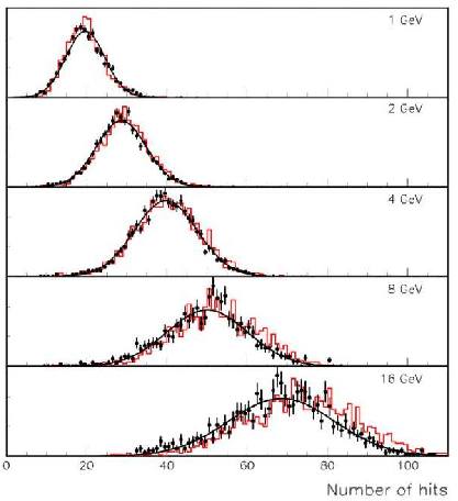
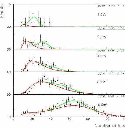
The response to positrons and pions was studied for beam momentum settings at 1, 2, 4, 8 and 16 GeV/c. The distribution of number of hits and the longitudinal and lateral shower shapes were measured [11, 12]. The results were compared to a Monte Carlo simulation of the set-up based on GEANT4. As an example Fig. 29 shows the number of hits obtained with positrons at the various beam settings. Notice the deficiency of hits at the higher momenta, due to the limited rate capability of RPCs.
The rate capability of RPCs was measured utilizing the 120 GeV primary proton beam at different intensities [17]. For rates above 100 Hz/cm2 a clear decrease in efficiency is observed. The group developed an analytical model which adequately reproduces the observed effects.
7.3 Current activities
Currently the collaboration is assembling a large prototype calorimeter, the physics prototype. The calorimeter will consist of 38 active layers interspersed with absorber plates. The latter will be provided by the Analogue Hadron Calorimeter (AHCAL) stage. Each layer will measure cm2 and contain three separate chambers. With a segmentation of cm2 laterally and layer-by-layer longitudinally, the calorimeter will count close to 400,000 readout channels.
The group is actively assembling chambers. Whenever possible the tasks are achieved with the help of jigs or fixtures. The spraying of the glass plates is performed within a spraying booth and is entirely automatic. The frames of extruded PVC are cut and predrilled (to allow for the insertion of the fishing lines, acting as spacers between the glass plates) using a specially designed jig. The RPCs are assembled within a fixture providing exact dimensions at the 25 - 50 m level.
The front-end ASICs, the DCAL III chips, have been produced and over 10,000 units are in hand. A handful of chips underwent extensive testing. No design faults have been discovered. The DCAL III chips are currently being tested by a robot at FNAL. Apart from the first wafer which showed a low yield, the average yield appears to be in excess of 90%. So far, the robot tested approximately half the 10,000 chips.
The front-end boards contain each 24 DCAL chips and cover an area of 32 x 48 cm2, see Fig. 30. The boards also contain the data concentrator seen in darker green on the left side. The board has been prototyped, the firmware written and debugged. The board was utilized to collect Cosmic ray data in conjunction with large chambers. A second round of prototyping is currently underway, before initiating mass production.
The data collector boards have been fabricated and assembled. Of the 35 boards about six have been tested so far. The performance is as expected. The timing and trigger module is currently undergoing a re-design. Prototypes of the new modules are expected within the next two months.
The high voltage system is in hand and its computer controlled program has been commissioned. A gas mixing rack has been assembled and successfully tested. The gas distribution rack utilized in the VST will undergo a minor extension to be used with the physics prototype. The low voltage power supplies are in hand. Power distribution boxes have been designed and a first prototype has been built.
To facilitate combined running with other CALICE calorimeter prototypes, the DHCAL DAQ software has been written within the framework of the CALICE DAQ software. The software is written and is currently used to collect Cosmic Ray data with the new boards.
Finally, the performance of the physics prototype has been simulated in great detail, including the actual response of RPCs [12].
The construction of the physics prototype is expected to be completed by April 2010, to be followed by a first test period in the FNAL test beam. Combined tests with the CALICE Silicon-Tungsten will take place in the late summer of 2010. A final running period is foreseen for early 2011.
7.4 Plans for the future
Despite the large effort of assembling the physics prototype the collaboration has initiated R&D concerning the remaining technical issues of an RPC-based hadron calorimeter. Table 1 summarizes the various (planned) activities.
| R&D topic | Funds | Comment |
|---|---|---|
| Thin RPC | Applied for | Further investigation of 1-glass design |
| Large area RPCs | Currently not pursued | Areas of several m2 needed |
| Gas system | Funded | Exploration of new gas mixtures, recycling, gas distribution |
| High Voltage distribution | Funded | System capable of supplying HV to all layers of a module individually |
| Low Voltage distribution | Currently not pursued | System capable of supplying LV to all layers of a module individually |
| Wedge shape | Currently not pursued | Develop concept to accommodate wedge shaped module designs |
| Pad/FE-board | Currently not pursued | Develop new design which minimizes thickness |
| Front-end ASIC | (Funded) | Develop next iteration with reduced power consumption, token ring passing, and redundancy for reliability |
| Data concentrator | Currently not pursued | Develop new system which minimizes space requirement and provides high reliability |
| Mechanical structure | Currently not pursued | Develop cassette structure which can be oriented which ever way, develop module structure which accommodates all supplies and data lines |
| Magnetic field | Currently not pursued | Tests of all subsystems in magnetic field |
7.5 GEM DHCAL Status
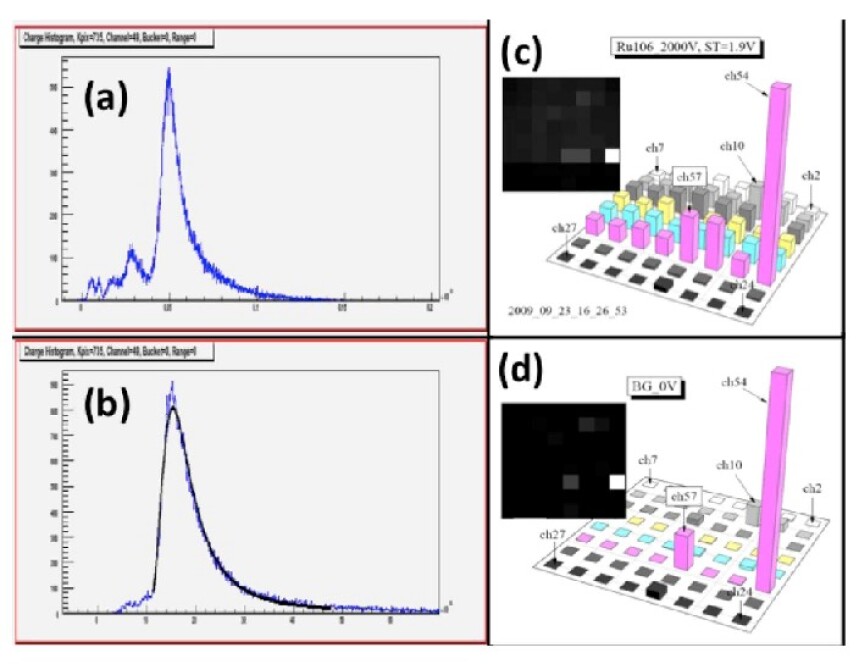
The University of Texas at Arlington HEP team has been developing a digital hadron calorimeter (DHCAL) using the Gas Electron Multiplier (GEM) as the sensitive gap technology. The team has constructed several prototype chambers to date and has completed constructing a new chamber, GEM4, with the new gas-transparent G10 spacer from CERN and the updated KPiX readout board. The team has been performing chamber characterization, using and radioactive sources. Figure 31(a) shows two distinct peaks from X-rays in one of the 64 KPiX readout channel. Figure 31(b) shows the Landau distributions from -particles from a source. The team is now working on two dimensional measurement. The sources were placed at a sufficient height to illuminate all active channels, demonstrating two dimensional profile distributions in Fig. 31(c). The three channels (54, 57 and 10) with a large number of hits arise from electronic noise as demonstrated clearly in Fig. 31(d), which shows the scatter plot of hits without high voltage supplied onto the chamber - the noise distribution is the same even with HV.
The team is in the process of investigating the uniformity of the chamber responses. The team will determine chamber gains using sources and will take cosmic ray data for further MIP studies and efficiency studies.
7.6 Future Plans for GEM DHCAL
In order to keep up progress toward a GEM based DHCAL, the UTA team plans a three-phased approach as described below.
7.6.1 Phase I: Through Late 2009
-
•
30 cm30 cm Chamber Characterization: Building on the successes accomplished in reading out multiple channels using 64 channel KPiX version 7 chip, the team will complete bench characterization of the chamber using radioactive sources and cosmic ray particles. The team then will take the chamber to a particle beam and take data to complete characterization of the chamber. At the same time, since the team plans to ultimately take data in the CALICE stack as a DHCAL, it will investigate the behaviour of the chamber using the DCAL digital readout chip jointly developed by ANL and FNAL.
-
•
33 cm100 cm Large GEM Foil Development: The team has been working with the CERN GDD workshop in developing 33 cm100 cm GEM foils, the largest to date, and finalized the design of 33 cm100 cm GEM foils that have the active area dimension of 32 cm96 cm and sent it to the CERN GDD workshop. The CERN GDD workshop has been successful in producing GEM foils with uniform hole shapes. The initial prototype run for 33 cm100 cm GEM foil was attempted in late August 2009 but the quality of the holes was unsatisfactory. CERN GDD has been working on refining the process and is ready for another run.
7.6.2 Phase II: Late 2009 – Late 2010
-
•
33 cm100 cm Unit Chamber Development: During this period, the team will certify GEM foils as they get delivered and will work on the assembly technique for 33 cm100 cm unit chambers.
-
•
Characterization of 1024 Channel KPiX Chips: The team plans to work on characterization of the 1024 channel KPiX chips with the intent to use them in 33 cm 100 cm unit chamber characterization. The latest 30 cm30 cm chamber will be used for chip characterization before assembling them in large unit chambers.
-
•
Understanding of Chamber Behaviour with DCAL Chips: The team will continue working on understanding the chamber behaviour with the DCAL chip, if this is not completed in the previous period.
-
•
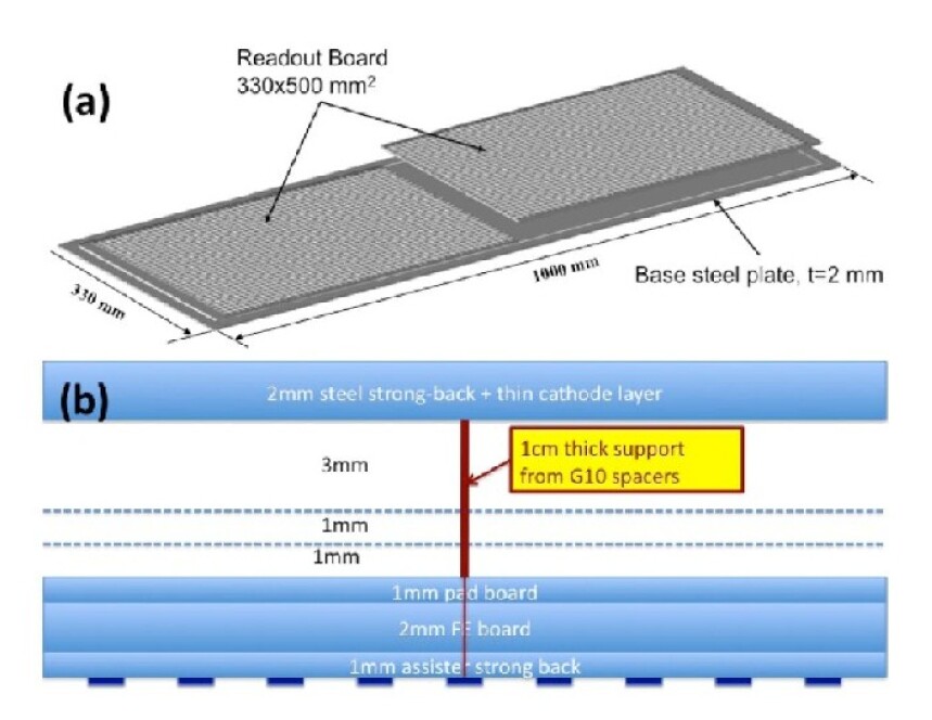
Begin Construction of 33 cm100 cm Unit Chambers: The team will begin construction of 33 cm100 cm unit chambers. The team plans to build one using the most understood KPiX chip-based anode boards to fully characterize 33 cm100 cm unit chambers. The team will build fifteen additional chambers with DCAL chip based anode boards to use them in assembling the final 100 cm100 cm DHCAL sensitive gap planes. Figure 32(a) shows a three dimensional schematic diagram of the unit chamber. It clearly shows the two readout boards of 33 cm50 cm since the flatness of the boards any longer than this size is not guaranteed. Figure 32(b) shows the cross section of a unit chamber. It shows that the total thickness of these chambers will be of the order of 11 mm, including a 2 mm steel plate that acts as a strong-back. The spacer has a 1 cm thick support in the middle of the chamber to provide sufficient surface area for the anode board to be glued on. We also plan to put another 1 mm thick strong-back support steel plates with holes that allows readout chips to protrude. This steel plate does not add any additional thickness to the overall dimension of the chamber.
7.6.3 Phase III: Mid 2010 – Late 2011
-
•
Unit Chamber Characterization with DCAL Chips: The team will characterize 33 cm100 cm unit chamber built with DCAL chip based anode board on the bench and in particle beams.
-
•
Construction of Five 100 cm100 cm Chamber Planes: The team will complete construction of all fifteen 33 cm100 cm unit chambers and complete assembling five 100 cm100 cm sensitive detector planes. The team plans to put three unit chambers together on a steel plate to provide mechanical strength to the 100 cm100 cm detector planes. These planes will be inserted into the existing CALICE calorimeter stack and run together with Si/W ECAL and 35 RPC planes in the HCAL. One critical constraint in this beam test is that the CALICE stack can stay at in the USA only until April 2011 due to customs rules.
-
•
TGEMs and RETGEMs: The team has also been looking into Thick GEM (TGEMs) and Resistive TGEMs (RETGEMs). Weizemann Institute in Israel has been collaborating with us in developing large size TGEMs. Thus, if these two new types of GEMs become available and if our resources allow, the team plans to explore the possibility of using these GEMs to produce chambers and beam test them.
8 Semi-digital HCAL: SDHCAL
8.1 Introduction
Members of the CALICE collaboration, including Belgian, Chinese, French, Russian and Spanish groups, are pursuing a new development aimed at constructing a highly granular gaseous hadronic calorimeter prototype based on a semi-digital readout and a transverse segmentation of 1 cm2. In addition to the tracking capability it offers, a semi-digital readout HCAL can provide very good energy resolution which can be, according to simulations, as good as that of an analogue calorimeter with an appropriate choice of threshold values. The semi-digital HCAL prototype is intended to come as close as possible to the hadronic calorimeters of the future ILC experiments in terms of resolution, efficiency and compactness.
Two kinds of gaseous detectors are being investigated as candidates to become the sensitive medium of such a SDHCAL: glass RPCs (GRPC) and Micromegas. New readout electronics satisfying the ILC constraints was developed and successfully tested on small GRPC detectors and more recently on a 1 m2 detector. Tests of small and medium size Micromegas detectors were also performed, yielding promising results. A 1 m 2 Micromegas prototype is under construction and will be tested in 2010.
8.2 GRPC detector development
GRPCs are well tested detectors. They have been successfully used in BELLE for almost a decade and more recently in OPERA and ALICE. Nonetheless, GRPCs to be used as the sensitive medium in the future HCAL need to be thinner than the standard ones in order to reduce the total radius of the hadronic calorimeter and hence the cost of the magnet coil inside which the HCAL should be placed. For this reason, GRPCs of 3 mm thickness were conceived and built. In addition to the thickness constraint, dead zones due to spacers used between the two glass plates of the GRPC are to be reduced. New schemes using tiny ceramic balls were introduced. This reduces the dead zones from a few percent to a negligible level. Another important point is the gas consumption in such a detector. New gas distribution designs were studied with the goal of renewing the gas efficiently, increasing the homogeneity and at the same time reducing the needed gas flow. Another R&D activity concerning the resistive coating of GRPCs is going on. Different coatings were tested to reduce the number of pads associated to one mip. This number was found to go from 1.6/mip in case of standard graphite coating to 1.3/mip for more resistive products like the Licron and Statguard products. To guarantee the homogeneity of the painting on detectors of large surface area silk screen printing techniques were successfully used. Stability of high voltage connections were also improved by using new gluing materials. Although the accumulated charge on the HCAL GRPCs in the future ILC experiments is expected to be very small, a few GRPCs are being exposed to high irradiation in the GIF facility at CERN to discover any eventual ageing effect.
A recent development has started recently to improve on the detection rate capacity. Due to the float glass resistivity (.cm) standard GRPCs can operate efficiently only with rates below 100 Hz/cm2. New semi-conductive glass (.cm) developed in China by the Tsinghua group was used to build small GRPCs. Exposure to pion beams at CERN has shown that the new GRPC can operate up to 30 kHz/cm2 with the same efficiency. This breakthrough in GRPC technique is an important achievement not only for future ILC experiments but also for ones like SLHC where very high rates are expected.
Using cosmic ray test benches or test beams at CERN, the efficiency of the different GRPCs was found to be more than 90% when operated in the high voltage range between 7 and 8 kV.
8.3 Micromegas detector development
The impressive progress made in the last decade on Micro Pattern Gaseous Detectors makes Micromegas a viable choice for a semi-digital hadronic calorimeter. This detector is used in several physics experiment: it is part of the COMPASS tracker, the T2K TPCs and is also a serious candidate for the upgrade of the ATLAS muon spectrometer at SLHC and for an ILC TPC.
Micromegas is a proportional gaseous detector and is therefore best suited for the application in a semi digital HCAL, the relation between readout signals and primary ionisation being strictly linear. It works in standard mixtures like Ar/iC4H10 and Ar/CO2 and at voltages below 500 V. Thanks to its mild amplification field (40 kV/cm) and the small size of the amplification gap (128 m) the rate capability of Micromegas is very high and its gas gain remains stable after a total accumulated charge as high as several mC/mm2. It is hence well suited for an experiment that should run for several decades.
With the Bulk fabrication technique developed and routinely used by the CERN technical service, large area and robust Micromegas can be made. To reduce the detector thickness to a minimum, the manufacturing process was modified to integrate on both side of a single PCB, the readout (digital front-end chips) and the amplification part (pads and mesh). With analog electronics, a detection efficiency to 100 GeV/c muons of 98 % was measured with a mean number of hits per traversing particle below 1.15. Micromegas thus satisfies the SDHCAL requirements of thickness, efficiency and pad multiplicity.
As all MPGD, Micromegas has a tendency to spark when operated at high gas gains. For that reason, additional passive components are connected with the front-end chips to the PCB and have shown to fully protect the electronics. Other implementations like buried resistors and capacitors and new protective methods and schemes are currently under investigation.
8.4 Electronics
To read out the gaseous detectors mentioned above an electronic chip called HARDROC with a semi-digital readout was developed and successfully tested. The chip has three thresholds (2-bit readout). It has 64 channels and each of the 64 channels is made of:
-
•
Fast low impedance preamplifier with a variable gain over 6 bits per channel
-
•
Variable shaper (50-150ns) and Track and Hold to provide a multiplexed analogue charge output up to 15pC.
-
•
3 variable gain fast shapers (15ns) followed by 3 low offset discriminators which allow handling wide dynamic range from 10fC up to 15pC. The thresholds are loaded by three internal 10-bit DACs.
In addition, the chip has a 128 deep digital memory to store the discriminators’ outputs and the bunch crossing identification coded over 24 bits counter. It is equipped with a power pulsing system which allows a consumption lower than 10W/channel to be reached with a 0.5% duty cycle. The cross-talk among the 64 channels was measured and found to be less than 2%.
In parallel to the development of HARDROC, another 64 channel ASIC called DIRAC was fabricated. It is intended for equipping both RPC and Micromegas and accordingly has two dynamic ranges: up to 10 pC or 200 fC. It has already been successfully tested in the latter detector. Each channel is equipped with a switched charge preamplifier, a switched baseline restorer and three comparators. The threshold of each comparator is set by an 8-bit DAC. The 2-bit result of the comparison is stored into an 8 event depth memory. Moreover, each event is stamped with a 12-bit identifier for bunch crossing identification. Configuration and readout signals are serial digital signals, this allow several ASICs to be chained in view of the construction of large area detectors.
The DIRAC is auto-triggered and designed so as to minimize the threshold dispersion over all channels and avoid any calibration. The measured dispersion is better than 1.17 fC (in the Micromegas mode) which is small compared to the typical MIP input charge of 25 fC. Its functioning is synchronous to a clock: signals are detected during the first half period of the clock while threshold comparison and memory writing occur in the second half period. This functioning together with power pulsing capability (10 W/channel) are intended to match the ILC beam time structure.
8.5 Small prototypes
To validate the concept of a semi-digital hadronic calorimeter, a Printed Circuit Board was developed to host 4 HARDROCs. The board provides the connection between adjacent chips as well as linking the first chip to the readout system. For simplification reasons the readout system using FPGA devices was also implemented on the same PCB as well as a USB device responsible of the communication between the FPGA and an external server. The PCB is an 8-layer , 800 m thick circuit. On one of the two PCB faces, 256 copper pads of 11 cm2 were printed. The distance between two adjacent pads was chosen to be 500 m. The cross-talk among adjacent pads was tested before other electronics components were fixed on the PCB by injecting a charge of 1 pC on one pad using an appropriate probe. The charges induced on the adjacent pads were then measured and found to be less than 0.3 %. Acquisition software was also developed. It permits the configuration parameters to be downloaded to the different chips and data to be collected from these chips through the FPGA device. Two readout modes were implemented. The first one is an ILC-Like one where events are recorded during the bunch crossings and the readout takes place after. The other mode was conceived for cosmic rays and beam test studies. In this mode the acquisition and data taking is stopped when an external trigger occurs. The memory of the different chips is then read out. In both modes each event is associated with a time stamp. In the external trigger mode the time difference between the external trigger and the last recorded event is also given. This determines the time occurrence of each event with respect to the external trigger one. The time precision is given by the HARDROC internal clock which runs at 5 MHz frequency.
The electronics boards described above were attached to small GRPCs and assembled together to form a small prototype of five chambers. The acquisition system was extended to deal with the data coming from each chamber and assemble them in events. A LABVIEW-based graphic interface was developed. This allowed an easy gain correction of all the channels. The setup was exposed first to cosmic rays and then to beams at CERN. The whole system performed very well and allowed the GRPC efficiency and multiplicity to be studied. Completed with 2 cm stainless steel plates, the setup was exposed to pions at the CERN PS to study the first phase of hadronic showers.
Several Micromegas prototypes equipped with analog or digital electronics and sizes between 88 cm2 up to 3248 cm2 were fabricated and tested in a beam at CERN SPS and PS. Prototypes with analog electronics were used for extensive characterisation in 2008. Signal distribution from high energy particles, uniformity, efficiency, pad multiplicity were measured. Their dependence on pressure, temperature and threshold variations are now fully understood. This work was summarized in a publication in JINST.
Tests of Micromegas chambers equipped with 1 DIRAC or 4 HARDROCs or 24 HARDROCs chips and a Detector Interface Board (so-called DIF) were performed in 2009. The data acquisition chain consists of the ASICs, the DIF, a USB cable and either the CrossDaq or LabView based software. The latter was developed for chip characterisation and recently for more flexible and efficient data taking. Multiplicity measurements are compatible with previous values from analog readout prototypes. The analysis of the collected data is on-going.
8.6 Technical prototypes
The success of the small prototype was the first step towards the construction of the technical prototype. The second and decisive step is to build a fully equipped detector of 1 m2. For this purpose, a new PCB hosting 24 ASICs was designed with the possibility to connect a few of them together. An independent interface board (DIF) connecting the PCB to the acquisition system was also produced and tested. Six such PCBs were produced and equipped. Every two PCBs were connected to each other and connected to one DIF. The six boards were fixed to a mechanical support made of stainless steel plate and then attached to a 1 m2 GRPC. The three DIFs connected to the PCBs are chained together and connected to a monitoring computer. An acquisition system using the Xdaq system developed by the CMS collaboration is used to build events from the collected data. A cosmic ray test bench was used to study the whole system. After a debugging period, the whole system works adequately. Few variants of GRPC were tested using the large electronic board in test beam at CERN in June and August 2009. The collected data were analysed. Synchronization among the different DIFs was successful and the data coherence demonstrated. The measured efficiency of the 1 m2 GRPC was found to be in the same range of those of small GRPC chambers(%). This success constitutes an important milestone in the validation of the SDHCAL. To complete this study an improved electronic board equipped with the new version of the HARDROC chips is under construction. The board will be attached to a 1 m2 GRPC and inserted into a cassette. This will be the first unit of the technical type to be built in 2010.
The 1 m2 Micromegas prototype is formed by 6 PCBs of 3248 cm2, each equipped with a mesh and 24 HARDROCs. These units are called Active Sensor Unit (ASU) and are placed into the same gas chamber with minimum dead areas between the ASUs. Our choice was to lay one mesh per ASU instead of a 1 m2 mesh on the 6 ASUs, essentially to avoid destructive sparks from the increased capacity of a too large area mesh. Moreover no facility can yet perform the complete bulk construction procedure over a 1 m2 area.
Before proceeding to the construction of a technical prototype, a mechanical prototype without electronics and mesh was assembled to check the gas tightness and validate the design and the complete assembly procedure. The technical prototype is now being assembled and will be tested in 2010 at CERN. The commissioning of the 6 ASUs has started a few months ago already. It consists of HV training in air and in gas, ASIC precise calibration, electronic chaining of the ASUs by pair, measurement of the response to 55Fe quanta and cosmic particles in a gas box. These steps are essential to insure the overall quality of the 1 m2 prototype and are now routinely performed in the lab. This same procedure will be also used for the fabrication of additional prototypes, based on HARDROC or DIRAC chips, in 2010.
The fine granularity of Micromegas chambers (1 cm2), its insensitivity to neutrons and its fast response are particularly interesting for a W-based HCAL for a multi-TeV range linear collider. Indeed, the shower separation in jets at CLIC will be more difficult than at ILC and a precise timestamping crucial. In view of a possible application in a CLIC HCAL, it is foreseen to equip a large scale tungsten structure with Micromegas layers.
8.7 Preparation for the 1 m3 technical prototype
The technical prototype will be made of 40 detectors interleaved with 2 cm stainless steel plates. The mechanical structure of the prototype is being currently designed. The aim is to have a self-supporting structure like the one proposed in the ILD and SiD concepts. The detectors with their readout boards will be assembled into cassettes that will be inserted between the Stainless Steel plates. The readout system will include data concentrators which will connect the DIF mentioned above to the general CALICE acquisition system. The development of data concentrators is almost finished and the whole readout system will be tested very soon to validate the whole chain. A gas distribution system controlling both the gas flow and pressure in the different chambers is under construction in collaboration with the CERN Gas Service. It will provide gas mixtures for RPCs (TFE/iC4H10/SF6) as well as for Micromegas (Ar/iC4H10 or Ar/CO2) chambers. High voltage power supplies using the Cockroft-Watson were designed and will be produced very soon. In the case of Micromegas which is works at voltages below 500 V, a CAEN crate with 40 HV channels is already available. The construction of the technical prototype is expected to start at the end of 2009 and to be completed by 2010. In addition to the hardware development, software activity is going on in order to prepare properly the comparison between data and the hadronic shower models used in the simulation.
9 Technical prototype front end electronics
A second generation of readout ASICs have been developed to read out the technical prototypes defined in EUDET and CALICE. These are based on the first generation of chips that were used for the physics prototype for the analogue front-end part but add several essential features:
-
•
Auto-trigger to reduce the data volume
-
•
Internal digitization to have only digital data outputs
-
•
Integrated readout sequence to minimize the number of lines between chips
-
•
Power-pulsing to reduce the power dissipation by a factor 100
Two chips have been designed, following the EUDET milestones:
-
•
HARDROC for digital hadronic calorimeters, using RPCs or micromegas chambers
-
•
SPIROC for analogue hadronic calorimeters and also for Si-W electromagnetic calorimeters.
Both chips have been successfully tested on testbench so that they are ready for tests with detectors. A third chio, SKIROC, has been partially developped, the analogue part, optimized for the ECAL, has been successfully tested earlier. A second version, with very large dynamic range and 64 channels, is underway.
Altogether these chips are being developped in an “industrialized” manner, with many building blocks in common, such that one design benefits from the experience with the other. The digital part was first developped and optimized with the HARDROC chip which is the simplest from the analogue point of view. SPIROC has a switch for the preamplifier characteristics which allows to toggle between usage for SiPM or silicon diode pad readout and is being uesed to proceed with the development of the Si-W ECAL technological prototype until the final SKIROC version is availabe.
9.1 DHCAL technical prototype: HARDROC ASIC
HARDROC readout is a semi-digital readout with three thresholds (2 bits readout) which allows both good tracking and coarse energy measurement, and also integrates on chip data storage. The chip integrates 64 channels of fast, low impedance current preamplifier with 6-bit variable gain (tuneable between 0 and 2 V), followed by a fast shaper (15 ns) and low offset discriminators. The discriminators feed a 128-deep digital memory to store the 264 discriminator outputs and bunch crossing identification coded by a 24-bit counter. Each is then read out sequentially during the readout period. A first version has been fabricated in AMS SiGe 0.35 m technology in September 2006 and met design specifications. A second version was produced in June 2008 to fit in a smaller low-height package (TWFP160) which necessitated changing the double-row bonding pad ring into a single row, rerouting all the inputs and removing many many pads. A possibility for a third threshold was added at that time, also separating more widely the three thresholds (typically 0.1–1–10 pC) and the “power off” state dissipation was brought down to a few W for the whole chip. The chip performance is shown in Fig. 33. The trigger efficiency allows the MIPs for RPCs to be discriminated with 100 fC threshold (10 fC for micromegas), with a noise of 1 fC. The power pulsing scheme has also been validated, also shown in Fig. 33, where 25 s are required to start up the chip so that it can trigger on a 10 fC input signal. Finally the readout scheme, which is common to all the chips has been valicated on the large square-meter board, built as a scalable technical prototype of the SDHCAL, that is readout from the side.
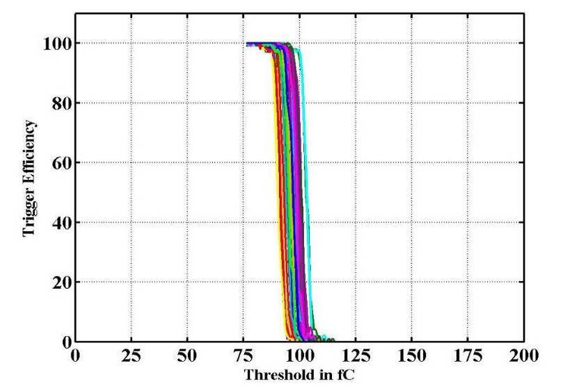
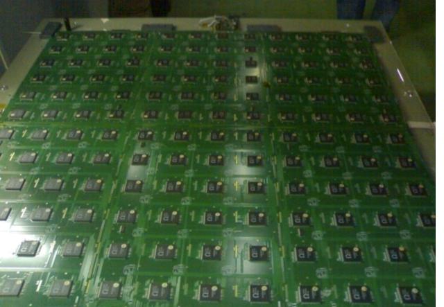
9.2 AHCAL technical prototype: SPIROC ASIC
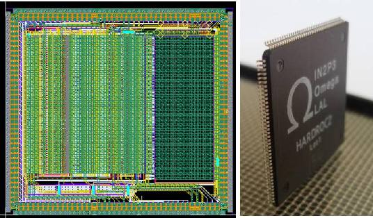
The SPIROC ASIC, which reads 36 SiPMs, is an evolution of the FLC_SiPM used in the AHCAL physics prototype. As for the ECAL, it keeps most of the analogue part, adding an analogue memory to record up to 16 events of a train and the auto-triggering capability. The digitization is implemented inside the chip as well as the data handling. The first prototype was fabricated in June 2007 in AMS SiGe 0.35 m. The chip layout is shown in Fig. 35. Its area is 35 mm2 for 36 channels and it is packaged in a CQFP240 package. Similarly to HARDROC, a second version has been realized in June 2008 to accommodate a thinner TQFP208 package and fix a bug in the ADC. The schematic diagram of one channel is shown in Fig. 36.
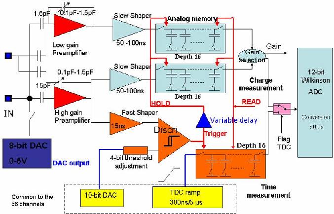
The main features are:
-
•
The 8-bit input DAC has been conserved, although its power dissipation has been brought down by 3 orders of magnitude to 1 W/channel as it is not power pulsed. The DAC also has the particularity of being powered with 5V whereas the rest of the chip is powered with 3.5V.
-
•
The voltage amplifier architecture with variable gain has also been kept, with a gain variable on 4 bits. However, the high gain/low gain separation is now done at the preamplifier level by having two preamplifiers in parallel on the input.
-
•
The charge is measured on both gains by a “slow” shaper (50–150 ns) followed by an analogue memory with a depth of 16 capacitors.
-
•
The auto-trigger is taken on the high gain path with a high-gain fast shaper followed by a low offset discriminator. All these blocks are new. The discriminator output is used to generate the hold on the 36 channels. The threshold is common to the 36 channels, given by a 10-bit DAC similar to the one from HARDROC with a subsequent 4-bit fine adjustment per channel.
-
•
The discriminator output is also used to store the value of a 300 ns ramp in a dedicated analogue memory to provide time information with an accuracy of 1ns
-
•
A 12-bit Wilkinson ADC is used to digitize the data at the end of the acquisition period.
The digital part is complex, as it must handle the write and read pointers, the ADC conversion, the data storage in a RAM and the readout process. The chip has been extensively tested since October 2007. The first series of tests has been mostly devoted to characterizing the analogue performance, which meets the design specifications. A single photoelectron spectrum displayed in Fig. 37 shows a photo-electron to noise ratio around 8. The auto-trigger is also shown in Fig. 37 and allows a threshold down to 50 fC to be tested.
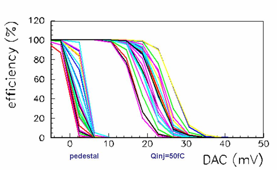
The digitization part has also been characterized and the 12-bit ADC exhibits a very good integral non-linearity of 1 LSB and a noise between 0.5 and 1 LSB.
The chips are now being assembled on an AHCAL PCB (HBU) and tested with the detector, as described in Sec. 6.
A new effort has been started to redesign the analogue input stage and further optimize it for SiPM readout. According to siumulations, it improves the signal-to-noise ratio by a factor 3 - 4. Once successfully tested with analogue chips, it is foreseen to integrate the design into the SPIROC architecure.
10 Technical prototype DAQ
The second generation data acquisition (DAQ) system follows an approach of using commercially-available hardware, where possible, with less dependency on bespoke equipment than has traditionally been the case in high energy physics and specifically in the previous CALICE DAQ system. The system is designed to be generic and hence applicable to many sub-detector systems and also to be able to provide the readout for the next generation of CALICE/EUDET prototype calorimeters. Indeed the CALICE calorimeters are an ideal test-bed as there are the different types (electromagnetic, hadronic, digital, etc.) with additional instrumentation also included during test-beam running such as small tracking systems. In principle, the DAQ system should be capable of reading out the final ILC calorimeter, with potential upgrades in chip flavor and network speed, but maintaining the basic architecture. Therefore the system should be easily upgradable, both in terms of ease of acquiring new components and competitive prices.
10.1 Overview of the DAQ system
An overview of the DAQ system is shown in Fig. 38; an explanation of each component is given below:
-
•
A control PC has the DAQ software (currently DOOCS [18], developed for XFEL) and will control the various DAQ PCs.
-
•
A customised DAQ PC is made from standard components but optimised for having two off-detector receiver (ODR) cards and also the large storage facilities which will be required.
-
•
The ODR is a commercial development board [19] with a large FPGA, optical fibers and a PCI Express bus. This can have a maximum of four optical fibers going to the next stage upstream.
-
•
The four optical fibers from the ODR will connect to the link data aggregator (LDA) which is a commercial FPGA development board [20] with add-on ethernet (to connect to the ODR) and HDMI (to connect upstream) boards. This is essentially a concentrator card which takes data from upstream on 10 HDMI links and merges them into one ethernet link to the ODR.
-
•
At the end of the calorimeter slabs, a detector interface (DIF) card is an electronics board which is specific to each calorimeter but converts the data into a common structure and format so that it is sent downstream, off the detector, in a uniform way. Each of the three DIFs in the present system (AHCAL, DHCAL and ECAL) is custom designed.
-
•
Providing the interface to the accelerator or a standalone clock is the clock and control card (CCC). This card was designed in-house due to the problems of finding commercially available systems which time-in several components all running with different clocks.
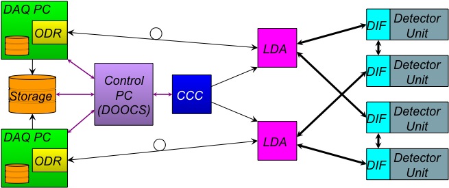
10.2 Status of the components
Overall, all electronics cards have been prototyped, where appropriate, and all are now in, or have finished, the production phase. Hardware orders are in place to ensure that we have enough systems available for laboratory, beam tests and spares. Significant blocks of firmware have been produced and final debugging of the whole DAQ chain is being performed. As well as the full chain which is being debugged in the UK, a complete system has been delivered to LLR to enable further debugging and integration with the detectors. The status of each component is discussed briefly below.
-
•
DIF: The ECAL DIF has been designed by UK groups and is now in production. This credit-card-sized board has been somewhat miniaturised from the prototype and the two production cards already manufactured are in use for the full system tests. To cover the expected need of 30 DIFs, 40 will be manufactured in the coming months. The AHCAL DIF and DHCAL DIF are the responsibility of the detector groups, primarily DESY and the French groups and are discussed in Sec. 6 and 8.
-
•
LDA: Final debugging of the DIFLDA link is ongoing. To cover the estimated 10 LDAs needed in test-beam running, 20 baseboards have been procured and 20 of each of the ethernet and HDMI add-on boards are on order.
-
•
CCC: At most, three CCCs will be needed at any one time; ten have been manufactured and tested and are ready for use. The one outstanding issue is the link from the CCC to the LDA. A small add-on PCB has been designed and is under test. Production will proceed after that and we expect to do this in-house as the design is so simple.
-
•
ODR and DAQ PC: As the ODR was the first component bought and the basis of the DAQ system, this has been stable for some time. Eight ODRs and six DAQ PCs have been purchased to provide for the expected need of four and three, respectively.
-
•
DAQ software: After an initial survey of available software by UK groups, it was decided to use the DOOCS system, developed by XFEL. Since responsibility of the software has been passed to LLR, this is being reconsidered, particularly in light of the possibility of combined test beams and as part of a common DAQ effort in the EU FP7 bid, AIDA.
The major issues still to be done for the DAQ system are:
-
•
Debugging the DIFLDA link which is the only link in the full system yet to be established.
-
•
Production of all final components, specifically manufacturing the DIFs and receipt of the LDA add-on boards from the manufacturer.
-
•
Finalise simple add-on PCB for CCC and LDA link.
-
•
Full documentation of components on the CALICE twiki (already started).
-
•
Archiving of all code in a central svn code repository (already started).
It is expected to achieve all of the above and hence have a working DAQ system with a full set of components (plus spares) by the end of the year. This will then allow the LLR group to set-up their system and integrate with the detector as well as then providing other detector groups with a system and spares.
11 Future test beam plans
11.1 Physics prototypes
The years 2010-11 will see the finalisation of the main physics prototype phase. As described above, a physics prototype of the DHCAL based on RPCs will be completed in the first half of 2010. As for previous testbeams including the AHCAL, there will be data taking in combination with the Si-W ECAL and the TCMT, as well as standalone DHCAL data taking. Including commissioning and calibration phases altogether 14 weeks of test beam time will be requested from FNAL. Within this 14 weeks, CALICE should be the primary beam user for about 8 weeks. The other 6 weeks can be spent with parasitic running or the setup of the experiment. The physics program to be conducted will be largely oriented on that which has been conducted in the corresponding data taking in the years 2006-09. In the combined running, the emphasis will be put on energy ranges in which it is expected to see signals in the electromagnetic part and the hadronic part (plus tail catcher) In the standalone running also low energy hadrons are to be collected as well as electrons. Priorities would have to be defined later on but the data which were already taken give good guidelines. It is also envisaged to replace a few layers of the DHCAL with GEMs as sensitive detectors. This may happen towards the beginning of 2011. This effort might face the constraint that due to customs regulations, the CALICE stage currently at FNAL is required to be shipped back to Europe in April 2011; in that case tests can be completed at CERN.
The one remaining detector which is yet to complete a physics prototype detector is the DECAL; this is expected to be achieved by 2012.
A new initiative has been started in order to study the properties of tungsten as aborber material, primarily for an HCAL at a multi-TeV collider, but possibly also for the ILC. In the versatile structure of the physics prototype the steel absorber plates can be replaced by tungsten plates. Tests with existing scintillator layers could start in 2011, tests with gaseous layers as they become available.
11.2 Technical prototypes
The previous sections indicate that the CALICE collaboration is entering a new phase of R&D in which readout technologies and mechanical designs do meet already many requirements of the operation in a detector for a Linear Collider. Several groups of the collaboration are already quite advanced and new full scale prototypes are expected towards the end of 2010. The finalisation of these prototypes will be preceded by a number of larger and smaller testbeam efforts which will allow for maturing the newly developed technologies. Examples for these test beam efforts are:
-
•
Testbeams with 1 units of the technical prototype of the SDHCAL (both GRPC and micromegas variants). These units might already be part of the production of the entire prototype.
-
•
For the analogue hadron calorimeter it is envisaged to have a smaller scale testbeam in 2009 to prepare for electronics commissioning followed by a so-called horizontal test in 2010 and a vertical test in 2011. This means the available equipment will be arranged to allow for the measurement of electromagnetic showers.
-
•
The Si-W ECAL is planning to make tests with single ASU towards the end of 2010 in an electron testbeam.
It has to be stressed that the primary goal of these prototypes is to study technological solutions for the calorimetry at the ILC. The strategy for the coming years should take this into account. Here the main keywords are power pulsing and the limited depth of the buffers in the VFE which allow only for data taking rates of the order of 100 Hz during a spill. In addition to the pure technological issues a physics program is to be pursued. This physics program is derived from those of the physics prototypes, taking the new technical constraints into account. It requires the operators of testbeam sites to actively respond to the needs of the CALICE (LC) testbeam data taking at an very early stage. As it is foreseeable that potential high statistics physics runs will take a considerable amount of time, and this will require the deployment of remote control at the experimental sites.
A first large scale testbeam with a fully equipped technical prototype of an SDHCAL can be expected towards spring 2011. It is still to be clarified in what proportion this SDCHAL will be equipped with the two technologies under study, namely using GRPCs or micromegas as sensitive devices. The CALICE collaboration will identify this on the basis of experience gained with the two technologies by laboratory studies and during test beam campaigns of the year 2009.
Ideally, the SDHCAL will be joined by an Si-W ECAL technical prototype by end of 2011. The running of an AHCAL technical prototype alone and together with the Si-W ECAL technical prototype is to follow. During the year 2010 mechanical interfaces between the different detector types will have to be defined. More general year 2010 is to be used to integrate the detector components with the newly developed DAQ systems in order to provide an efficient data taking.
The program which is summarised in Table 2 requires a high availability of testbeam areas The CALICE management and the CALICE TB together with the corresponding ILC R&D panels will work out until December 2009 whether ILC detector R&D can occupy consecutively testbeam areas for a time of two or more years starting with the beginning of 2011. Such a high availability of testbeam areas would also allow for an easier conduction of smaller testbeam programs as for example with the DECAL, which has had a somewhat uncertain time scale due to funding issues in the UK. In addition a well functional infrastructure would facilitate the testing of a prototype for the electromagnetic calorimeter based on scintillating tiles (Sc-W ECAL) of which one layer can be expected towards the end of 2012. Finally, technological prototype layers with timing capabilities should also be used in a beam test with a tungsten absorber structure.
| Project | 2010/1 | 2010/2 | 2011/1 | 2011/2 | 2012/1 | 2012/2 |
|---|---|---|---|---|---|---|
| Phys. Prot. Si-W ECAL/DCHAL/TCMT | xx | xx | xx | - | - | - |
| Phys. Prot. W ECAL / W HCAL / TCMT | x | x | xx | xx | - | |
| Tech. Prot. DHCAL | x | x | xx | xx | xx | xx |
| Tech. Prot. AHCAL | x | x | x | x | xx | xx |
| Tech. Prot. Si-W ECAL | - | x | x | xx | xx | xx |
| Phys. Prot. DECAL | x | x | x | x | x | x |
| Tech. Prot. Sc-W ECAL | - | - | - | - | - | x |
As a concluding remark it needs to be stressed that the time plans presented here depend essentially on the available funding to complete the various prototypes. Thus, the actual running of, in particular, the test beams with fully equipped prototypes could easily be delayed by one year with respect to the dates indicated in Table 2.
12 Conclusions and request
CALICE has successfully completed a first round of data taking at CERN and Fermilab with physics prototypes for silicon based ECAL and scintillator based ECAL and HCAL. The detectors show the expected performance and the test beam data start to provide constraints in hadronic shower models. The beam test of a gaseous digital HCAL prototype is under preparation and supposed to start mid 2010. The physics program will the be extended towards the study of tungsten as absorber material.
Various technological prototypes are under preparation and in different stages of commissioning or beam test with detector elements. A program has been set up to demonstrate the viability of the designs with larger structures exposed to beams. Novel technologies like the digital ECAL have also undergone first tests with encouraging results.
We are asking the PRC for endorsement of this program and in particular its scope of technologies and its timeliness with respect to the ILC schedule.
We request the continuation of DESY’s support for test beam campaigns at Fermilab and CERN, for the adaptation of the set-up to new devices, for the continuation of electronics integration development towards completion of technological demonstrator prototypes, and for the continued provision of computing resources.
13 Acknowledgments
We would like to thank the technicians and the engineers who contributed to the design and construction of the prototypes. We also gratefully acknowledge the DESY, CERN and FNAL managements for their support and hospitality, and their accelerator staff for the reliable and efficient beam operation.
We would like to thank the HEP group of the University of Tsukuba for the loan of drift chambers for the DESY test beam. The authors would like to thank the RIMST (Zelenograd) group for their help and sensors manufacturing. This work was supported by the Bundesministerium für Bildung und Forschung, Germany; by the the DFG cluster of excellence ‘Origin and Structure of the Universe’ of Germany ; by the Helmholtz-Nachwuchsgruppen grant VH-NG-206; by the BMBF, grant no. 05HS6VH1; by the Alexander von Humboldt Foundation (Research Award IV, RUS1066839 GSA); by joint Helmholtz Foundation and RFBR grant HRJRG-002, Russian Agency for Atomic Energy, ISTC grant 3090; by Russian Grants SS-1329.2008.2 and RFBR0402/17307a and by the Russian Ministry of Education and Science; by MICINN and CPAN, Spain; by CRI(MST) of MOST/KOSEF in Korea; by the US Department of Energy and the US National Science Foundation; by the Ministry of Education, Youth and Sports of the Czech Republic under the projects AV0 Z3407391, AV0 Z10100502, LC527 and LA09042 and by the Grant Agency of the Czech Republic under the project 202/05/0653; and by the Science and Technology Facilities Council, UK.
14 Appendix 1: The CALICE Collaboration
C. Adloff,
J. Blaha,
J.-J. Blaising,
M. Chefdeville,
C. Drancourt,
A. Espargliere,
R. Gaglione,
N. Geoffroy,
Y. Karyotakis,
J. Prast,
G. Vouters
Laboratoire d’Annecy-le-Vieux de Physique des Particules, Université de Savoie,
CNRS/IN2P3,
9 Chemin de Bellevue BP110, F-74941 Annecy-le-Vieux Cedex, France
T. Cundiff,
G. Drake,
B. Haberichter,
V. Guarino,
A. Kreps,
E. May,
J. Repond,
J. Schlereth,
J. Smith222Also at University of Texas, Arlington,
D. Underwood,
K. Wood,
L. Xia,
Q. Zhang
Argonne National Laboratory,
9700 S. Cass Avenue,
Argonne, IL 60439-4815,
USA
A. Brandt, H. Brown, K. De, C. Medina, J. Smith, J. Li, M. Sosebee, A. White,
J. Yu
Department of Physics, SH108, University of Texas, Arlington, TX 76019, USA
Z. Deng, Y. Li, Wang Yi, Q. Yue, Z. Yang
Tsinghua University, Department of Engineering Physics.Beijing, 100084, P.R.
China
T. Buanes, G. Eigen, D. Fehlker, R. Roehrich, H. Sandaker
University of Bergen, Inst. of Physics, Allegaten 55, N-5007 Bergen, Norway
Y. Mikami,
O. Miller,
N. K. Watson,
J. A. Wilson
University of Birmingham,
School of Physics and Astronomy,
Edgbaston, Birmingham B15 2TT, UK
J. Butler, E. Hazen, S. Wu
Boston University, Department of Physics, 590 Commonwealth Ave.,
Boston, MA 02215, USA
M. J. Goodrick,
T. Goto,
L. B. A. Hommels,
J. S. Marshall,
M. A. Thomson,
D. R. Ward,
University of Cambridge, Cavendish Laboratory, J J Thomson Avenue, CB3 0HE, UK
D. Benchekroun,
A. Hoummada,
Y. Khoulaki
Université Hassan II Aïn Chock, Faculté des sciences. B.P. 5366 Maarif, Casablanca, Morocco
J. Apostolakis,
F. Duarte Ramos,
K. Elsener,
G. Folger,
A. Gaddi,
H. Gerwig,
C. Grefe
W. Klempt,
L. Linssen,
D. Perini,
A. Ribon,
A. Sailer,
D. Schlatter,
P. Speckmayer,
V. Uzhinskiy
CERN, 1211 Genève 23, Switzerland
M. Oreglia
University of Chicago, Dept. of Physics, 5720 So. Ellis Ave., KPTC 201 Chicago,
IL 60637-1434, USA
M. Benyamna,
N. Brun,
C. Cârloganu,
P. Gay,
S. Manen,
L. Royer
Laboratoire de Physique Corpusculaire de Clermont-Ferrand (LPC),
24 avenue des Landais,
63177 Aubière CEDEX, France
J. Ha
Korea Atomic Energy Research Institute,
Taejon 305-600,
South Korea
F. Abu-Ajamieh.
G. C. Blazey
D. Chakraborty
A. Dyshkant
K. Francis
D. Hedin
J. Hill
G. Lima
R. Salcido
V. Rykalin
V. Zutshi
NICADD, Northern Illinois University,
Department of Physics,
DeKalb, IL 60115,
USA
V. Astakhov, V. A. Babkin, S. N. Bazylev, Yu. I. Fedotov, S. Golovatyuk, I. Golutvin, N. Gorbunov,
A. Malakhov, S. Slepnev, I. Tyapkin, S. V. Volgin, Y. Zanevski, A. Zintchenko
Joint Institute for Nuclear Research, Joliot-Curie 6,
141980, Dubna,
Moscow Region, Russia
D. Dzahini,
L. Gallin-Martel,
J. Giraud,
D. Grondin,
J. -Y. Hostachy,
K. Krastev,
L. Morin,
F-E. Rarbi
Laboratoire de Physique Subatomique et de Cosmologie - Université Joseph Fourier Grenoble 1 -
CNRS/IN2P3 - Institut Polytechnique de Grenoble,
53, rue des Martyrs,
38026 Grenoble CEDEX, France
N. D’Ascenzo,
S. Christen,
U. Cornett,
D. David,
R. Fabbri,
G. Falley,
K. Gadow,
E. Garutti,
P. Göttlicher,
S. Karstensen,
F. Krivan,
K. Kschioneck,
A. -I. Lucaci-Timoce,
B. Lutz,
N. Meyer,
S. Morozov,
V. Morgunov,
M. Reinecke,
F. Sefkow,
P. Smirnov,
A. Vargas-Trevino,
N. Wattimena,
O. Wendt
DESY, Notkestrasse 85,
D-22603 Hamburg, Germany
N. Feege,
J. Haller,
S. Richter,
J. Samson
Univ. Hamburg,
Physics Department,
Institut für Experimentalphysik,
Luruper Chaussee 149,
22761 Hamburg, Germany
A. Kaplan, H. -Ch. Schultz-Coulon, W. Shen, R. Stamen, A. Tadday
University of Heidelberg, Fakultat fur Physik und Astronomie,
Albert Uberle Str. 3-5 2.OG Ost,
D-69120 Heidelberg, Germany
B. Bilki, E. Norbeck, Y. Onel
University of Iowa, Dept. of Physics and Astronomy,
203 Van Allen Hall, Iowa City, IA 52242-1479, USA
E. J. Kim
Chonbuk National University, Jeonju, 561-756, South Korea
G. Kim, D-W. Kim, K. Lee, S. C. Lee
Kangnung National University, HEP/PD, Kangnung, South Korea
B. van Doren,
G. W. Wilson
University of Kansas, Department of Physics and Astronomy,
Malott Hall, 1251 Wescoe Hall Drive, Lawrence, KS 66045-7582, USA
K. Kawagoe
Department of Physics, Kobe University, Kobe, 657-8501, Japan
P. D. Dauncey,
Imperial College, Blackett Laboratory,
Department of Physics,
Prince Consort Road,
London SW7 2AZ, UK
V. Bartsch333Now at University of Sussex, Physics and Astronomy Department, Brighton, Sussex, BN1 9QH, UK,
M. Postranecky, M. Warren, M. Wing
Department of Physics and Astronomy, University College London,
Gower Street,
London WC1E 6BT, UK
V. Boisvert,
B. Green,
A. Misiejuk,
F. Salvatore444Now at University of Sussex, Physics and Astronomy Department, Brighton, Sussex, BN1 9QH, UK
Royal Holloway University of London,
Dept. of Physics,
Egham, Surrey TW20 0EX, UK
E. Cortina Gil,
S. Mannai,
G. Nuessle
Center for Particle Physics and Phenomenology (CP3)
Université catholique de Louvain, Belgium
M. Bedjidian
A. Bonnevaux,
C. Combaret,
J. Fay,
G. Grenier,
J.C. Ianigro,
R. Kieffer,
N. Lumb,
I. Laktineh,
P. Lebrun,
H. Mathez,
M. Vander Donckt,
S. Vanzetto
Université de Lyon, F-69622, Lyon, France ;
Université de Lyon 1, Villeurbanne ;
CNRS/IN2P3, Institut de Physique Nucléaire de Lyon
E. Calvo Alamillo, M. C Fouz, J. Puerta-Pelayo
CIEMAT, Centro de Investigaciones Energeticas, Medioambientales y Tecnologicas, Madrid. Spain
D. S. Bailey,
R. J. Barlow,
R. J. Thompson
The University of Manchester, School of Physics and Astronomy,
Schuster Lab,
Manchester M13 9PL,
UK
M. Batouritski,
O. Dvornikov,
Yu. Shulhevich,
N. Shumeiko,
A. Solin,
P. Starovoitov,
V. Tchekhovski,
A. Terletski
National Centre of Particle and High Energy Physics of the
Belarusian State University, M.Bogdanovich str. 153, 220040 Minsk, Belarus
F. Corriveau
Department of Physics, McGill University,
Ernest Rutherford Physics Bldg.,
3600 University Ave.,
Montréal, Quebec,
CANADA H3A 2T8
V. Balagura, B. Bobchenko,
M. Danilov,
R. Mizuk, E. Novikov, V. Rusinov, E. Tarkovsky
Institute of Theoretical and Experimental Physics, B. Cheremushkinskaya ul. 25,
RU-117218 Moscow, Russia
V. Andreev, N. Kirikova, A. Komar, V. Kozlov, M. Negodaev, P. Smirnov, Y. Soloviev, A. Terkulov
P. N. Lebedev Physical Institute,
Russian Academy of Sciences,
117924 GSP-1 Moscow, B-333, Russia
P. Buzhan, B. Dolgoshein, A. Ilyin, V. Kantserov, V. Kaplin, A. Karakash, E. Popova, S. Smirnov
Moscow Physical Engineering Inst., MEPhI,
Dept. of Physics,
31, Kashirskoye shosse,
115409 Moscow, Russia
N. Baranova,
E. Boos,
L. Gladilin,
D. Karmanov,
M. Korolev,
M. Merkin,
A. Savin,
A. Voronin
M.V.Lomonosov Moscow State University, D.V.Skobeltsyn Institute of Nuclear
Physics (SINP MSU),
1/2 Leninskiye Gory, Moscow, 119991, Russia
A. Topkar
Bhabha Atomic Research Center,
Mumbai 400085, India
C. Kiesling,
S. Lu,
O. Reimann,
K. Seidel,
F. Simon
C. Soldner,
L. Weuste
Max Planck Inst. für Physik,
Föhringer Ring 6,
D-80805 Munich, Germany
J. Bonis,
B. Bouquet,
S. Callier,
P. Cornebise,
Ph. Doublet,
F. Dulucq,
M. Faucci Giannelli,
J. Fleury,
G. Guilhem,
H. Li,
G. Martin-Chassard,
F. Richard,
Ch. de la Taille,
R. Poeschl,
L. Raux,
N. Seguin-Moreau,
F. Wicek,
Z. Zhang
Laboratoire de L’accélerateur Linéaire,
Centre d’Orsay, Université de Paris-Sud XI,
BP 34, Bâtiment 200,
F-91898 Orsay CEDEX, France
M. Anduze,
K. Belkadhi,
V. Boudry,
J-C. Brient,
C. Clerc,
R. Cornat,
D. Decotigny,
F. Gastaldi,
D. Jeans,
A. Karar,
P. Mora de Freitas,
G. Musat,
M. Reinhard,
A. Rougé,
M. Ruan,
J-Ch. Vanel,
H. Videau
Laboratoire Leprince-Ringuet (LLR) – École Polytechnique,
CNRS/IN2P3,
Palaiseau, F-91128 France
K-H. Park
Pohang Accelerator Laboratory, Pohang 790-784, South Korea
J. Zacek
Charles University, Institute of Particle & Nuclear Physics,
V Holesovickach 2,
CZ-18000 Prague 8, Czech Republic
J. Cvach,
P. Gallus,
M. Havranek,
M. Janata,
J. Kvasnicka,
M. Marcisovsky,
I. Polak,
J. Popule,
L. Tomasek,
M. Tomasek,
P. Ruzicka,
P. Sicho,
J. Smolik,
V. Vrba,
J. Zalesak
Institute of Physics, Academy of Sciences of the Czech Republic, Na Slovance 2,
CZ-18221 Prague 8, Czech Republic
Yu. Arestov
V. Ammosov, B. Chuiko, V. Gapienko,
Y. Gilitski,V. Koreshev, A. Semak, Yu. Sviridov, V. Zaets
Institute of High Energy Physics,
Moscow Region,
RU-142284 Protvino,
Russia
B. Belhorma, M. Belmir, H. Ghazlane
Centre National de l’Energie, des Sciences et des Techniques Nucléaires,
B.P. 1382, R.P. 10001, Rabat, Morocco
R. Coath, J. P. Crooks,M. Stanitzki, J. Strube, R. Turchetta, M. Tyndel, Z. Zhang
Rutherford Appleton Laboratory, Chilton, Didcot,
Oxon OX110QX, UK
M. Barbi
University of Regina,
Department of Physics,
Regina, Saskatchewan,
Canada S4S 0A2
S. W. Nam, I. H. Park, J. Yang
Ewha Womans University, Dept. of Physics,
Seoul 120,
South Korea
Jong-Seo Chai, Jong-Tae Kim, Geun-Bum Kim
Sungkyunkwan University,
300 Cheoncheon-dong, Jangan-gu, Suwon, Gyeonggi-do 440-746, South Korea
Y. Kim
Korea Institute of Radiological and
Medical Sciences,
215-4 Gangeung-dong,
Nowon-gu, Seoul 139-706,
SOUTH KOREA
J. Kang, Y. -J. Kwon
Yonsei University, Dept. of Physics,
134 Sinchon-dong,
Sudaemoon-gu, Seoul 120-749,
South Korea
Ilgoo Kim, Taeyun Lee, Jaehong Park, Jinho Sung
School of Electric Engineering and Computing Science, Seoul National University,
Seoul 151-742, South Korea
S. Itoh, K. Kotera, M. Nishiyama, T. Takeshita
Shinshu Univ. ,
Dept. of Physics,
3-1-1 Asaki,
Matsumoto-shi, Nagano 390-861,
Japan
A. Khan, D. H. Kim, J.E. Kim, D. J. Kong, Y.D. Oh, S. Uozumi
Kyungpook National Univ., Dept. of Physics, 1370 San Kyuk-dong, Puk ku, Taegu 635, SOUTH KOREA
H. Koike,
Y. Sudo,
Y. Takahashi,
K. Tanaka,
F. Ukegawa
University of Tsukuba, Graduate School of Pure and Applied Sciences,
Tennoudai 1-1-1, Tsukuba, Ibaraki 305-8571, Japan
S. Weber, C. Zeitnitz
Bergische Universität Wuppertal
Fachbereich 8 Physik,
Gaussstrasse 20,
D-42097 Wuppertal, GERMANY
References
- [1] J.Repond et al., “Design and Electronics Commissioning of the Physics Prototype of a Si-W Electromagnetic Calorimeter for the International Linear Collider”, JINST 3, P08001 (2008).
- [2] J.Repond et al., “Response of the CALICE Si-W Electromagnetic Calorimeter Physics Prototype to Electrons”, Nucl. Inst. and Meth. A608, 372 (2009).
-
[3]
“Electron data with the CALICE tile AHCAL prototype
at the CERN test-beam”, CALICE Analysis Note CAN-014,
https://twiki.cern.ch/twiki/pub/CALICE/CaliceAnalysisNotes/CAN-014.pdf. -
[4]
“Preliminary results from hadron shower data with
the CALICE tile AHCAL prototype”, CALICE Analysis Note CAN-011, Addendum E,
https://twiki.cern.ch/twiki/pub/CALICE/CaliceAnalysisNotes/CAN-011e.pdf. -
[5]
“Preliminary results from hadron shower data with
the CALICE tile AHCAL prototype”, CALICE Analysis Note CAN-011, Addendum D,
https://twiki.cern.ch/twiki/pub/CALICE/CaliceAnalysisNotes/CAN-011d.pdf. -
[6]
“Initial Study of Hadronic Energy Resolution in the
Analogue HCAL and the Complete CALICE Setup”, CALICE Analysis Note CAN-015,
https://twiki.cern.ch/twiki/pub/CALICE/CaliceAnalysisNotes/CAN-015.pdf. -
[7]
“First Stage Analysis of the Energy response and
resolution of the
Scintillator ECAL in the Beam Test at FNAL, 2008”, CALICE Analysis Note
CAN-016,
https://twiki.cern.ch/twiki/pub/CALICE/CaliceAnalysisNotes/CAN-016.pdf. -
[8]
”Particle Flow Calorimetry and PandoraPFA algorithm” , M.A.Thomson,
arXiv:0907.3577(2009), submitted to Nucl. Instr. Meth. - [9] ”JRA3 Hadronic calorimeter Technical Design Report” , K. Gadow et. al, EUDET memo, (2008).
-
[10]
“Calibration of the scintillator hadron calorimeter of ILD”,
CALICE Analysis Note CAN-018,
https://twiki.cern.ch/twiki/pub/CALICE/CaliceAnalysisNotes/CAN-018.pdf. - [11] B.Bilki et al., “Measurement of positron showers with a digital hadron calorimeter”, JINST 4, P04006 (2009).
- [12] B.Bilki et al., “Hadron showers in a digital hadron calorimeter”, JINST 4, P10008 (2009).
- [13] SPiDeR Collaboration, N.K.Watson et al., “DESY PRC Report”, Oct 2009.
- [14] www.hep.anl.gov/repond/DHCAL.html.
- [15] G.Drake et al., “Resistive Plate Chambers for hadron calorimetry: Tests with analog readout”, Nucl. Inst. Meth. A578, 88 (2007).
- [16] B.Bilki et al., “Calibration of a digital hadron calorimeter with muons”, JINST 3, P05001 (2008)
- [17] B.Bilki et al., “Measurement of the rate capability of Resistive Plate Chambers”, JINST 4, P06003 (2009).
- [18] doocs.desy.de.
- [19] Component “Xpress FX100”, www.plda.com.
- [20] Component “Mulldonnoch2”, www.enterpoint.co.uk.