Magneto-transport in Disordered Graphene:
from Weak Localization to Strong Localization
Abstract
We present a magneto-transport study of graphene samples into which a mild disorder was introduced by exposure to ozone. Unlike the conductivity of pristine graphene, the conductivity of graphene samples exposed to ozone becomes very sensitive to temperature: it decreases by more than 3 orders of magnitude between 100 K and 1 K. By varying either an external gate voltage or temperature, we continuously tune the transport properties from the weak to the strong localization regime. We show that the transition occurs as the phase coherence length becomes comparable to the localization length. We also highlight the important role of disorder-enhanced electron-electron interaction on the resistivity.
I Introduction
Quantum interference phenomena in graphene are of fundamental interest McCann2009 . A case in point is the localization of charges, which is a manifestation of two important properties of this material: First, graphene hosts chiral Dirac fermions. Second, these fermions reside in two inequivalent valleys at the K and K′ points of the first Brillouin zone. Traveling paths that are relevant to localization phenomena are phase coherent closed loops. Because of its chirality, a Dirac fermion residing in a given valley acquires a phase of upon completion of one loop, which gives rise to destructive interference with its time-reversed counterpart. Chirality therefore lowers the probability for returning paths, and favors weak antilocalization. Restoring constructive interferences requires inter-valley scattering events (fermions in the K and K′ valleys have opposite chiralities). This in turn favors weak localization.
These quantum interference effects have been actively studied both theoretically Suzuura_Ando_JPSJ ; Aleiner ; Altland ; Mirlin ; McCann_PRL06 ; Morpurgo and experimentally Geim ; deHeer ; Savchenko2008 ; Savchenko2009 ; Mason . It has been predicted that weak localization correction to the semi-classical (Drude) conductivity will dominate the weak antilocalization correction as the temperature is lowered, driving graphene to the strong localization regime Aleiner . Surprisingly however, these corrections measured in graphene samples have remained modest, even at milliKelvin temperatures.
A clear strategy to study the transition between weak localization and strong localization is to enhance intervalley scattering. This can be achieved by introducing short-range scatterers, such as weak point disorder or lattice defects that result in midgap states das_Sarma ; Ando ; Guinea . Recently, defect scattering centers were introduced in graphene using Ne and He ion irradiation, but the conductivity at the Dirac point remained above even down to cryogenic temperature ( is the conductivity value for which the weak localization regime is expected to cross over to the strong localization one Fuhrer_PRL09 ).
Approaches to drive the metallic phase of graphene to an insulator with an energy band gap have also been explored. In the case of graphane Geim_Science09 , bonds were partially transformed into by hydrogenation. There, the resistivity was found to diverge at low temperatures, in accordance with the two-dimensional variable range hopping model. The measurements were interpreted as the result of a modified graphene that consists of two phases, regions with hybridization interspersed with regions Geim_Science09 . Similar results were obtained with oxidized graphene Gomez-Navarro_NL07 ; Kaiser_NL09 . Another work reported transport measurements deep in the strong localization regime using graphene modified with hydrogen atoms Bostwick .
Overall, these transport studies on intentionally disordered graphene focused either on the metallic regime Fuhrer_PRL09 or on the deep localization regime, where the material behaves as an insulator Geim_Science09 ; Gomez-Navarro_NL07 ; Kaiser_NL09 ; Bostwick . The possible transition between weak localization and strong localization remains to be explored.
In this work, we report on a detailed magneto-transport study unveiling quantum localization effects in disordered graphene. Disorder is created by exposing graphene to ozone, which introduces sp3-type defects. By varying either an external gate voltage or temperature, we continuously tune the transport properties from the weak localization to the strong localization regime. We show that the transition occurs as the phase coherence length becomes comparable to the localization length. In addition, we evidence a marked contribution of electron-electron interaction to the resistivity. (This latter effect is a correction to the density of states and its origin differs from the one of weak localization, which stems from a modification of the diffusion constant Beenakker ).
II Experimental results
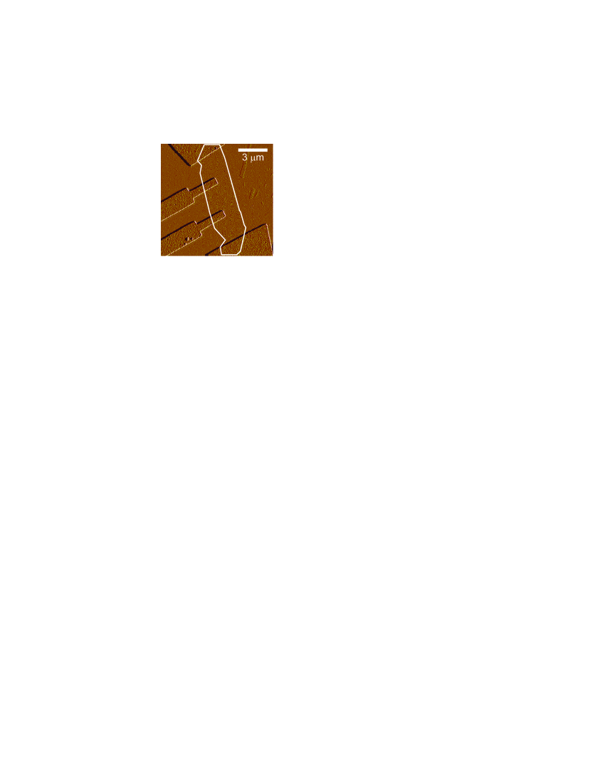
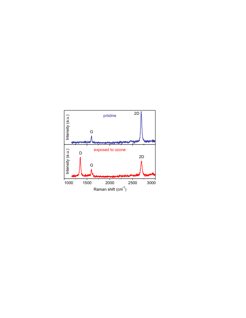
Before creating defects in graphene, we first fabricate high-quality devices using conventional nanofabrication techniques (Fig. 1) APL_cleaning . We mechanically exfoliate graphene from a flake of Kish graphite on a Si wafer coated with 300 nm of thermal oxide. We pattern Cr/Au electrodes in a four-point configuration using electron-beam lithography. We carry out Raman spectroscopy ferrari and low temperature transport measurements to verify that single layer graphene sheets are of good quality. For the device discussed in the paper, the D peak is absent before ozone treatment (Fig. 2, upper panel). In addition, the mobility is , and the conductivity at the Dirac point reaches and is temperature independent down to liquid helium temperatures (not shown).
We introduce defect using an ozone treatment, which is a chemically reactive process known to alter the underlying network of graphitic systems Lee_JPC09 . Specifically, we first clean graphene samples by placing them in a flow of Ar/H2 gas at for 3 hours. We then expose the samples to ozone in a Novascan ozone chamber, where ozone is produced by ultra-violet irradiation of O2 gas ( min, 4 atm). The appearance of the D peak in the Raman spectrum (Fig. 2, lower panel) and the decrease of the mobility down to (see below) signal the creation of additional defects. However, we make sure that the ozone treatment is mild enough to preserve the crystalline integrity of graphene, as evidenced by the presence of the G peak and a well defined 2D peak in Raman spectroscopy. In addition, the elastic mean-free path of electrons estimated from the Drude conductivity is at least 3 nm (see below), which is more than one order of magnitude larger than the C-C bond length.
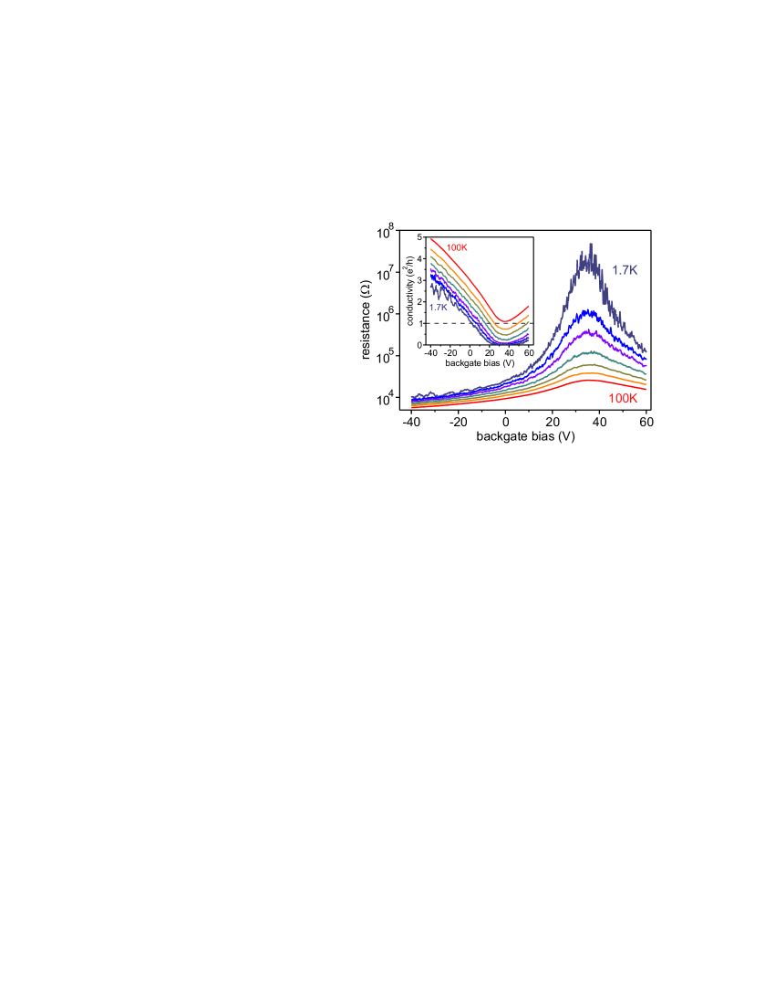
This ozone treatment has a large impact on the transport properties of graphene. The conductivity becomes very sensitive to temperature (Fig. 3). Even though the conductivity at the Dirac point remains larger than at the highest temperature (100 K), it is reduced by more than 3 orders of magnitude at 1.7 K. The device behaves as an insulator, at least at low temperature and in the vicinity of the Dirac point (where the conductivity as a function of backgate bias is lowest, see inset to Fig. 3).
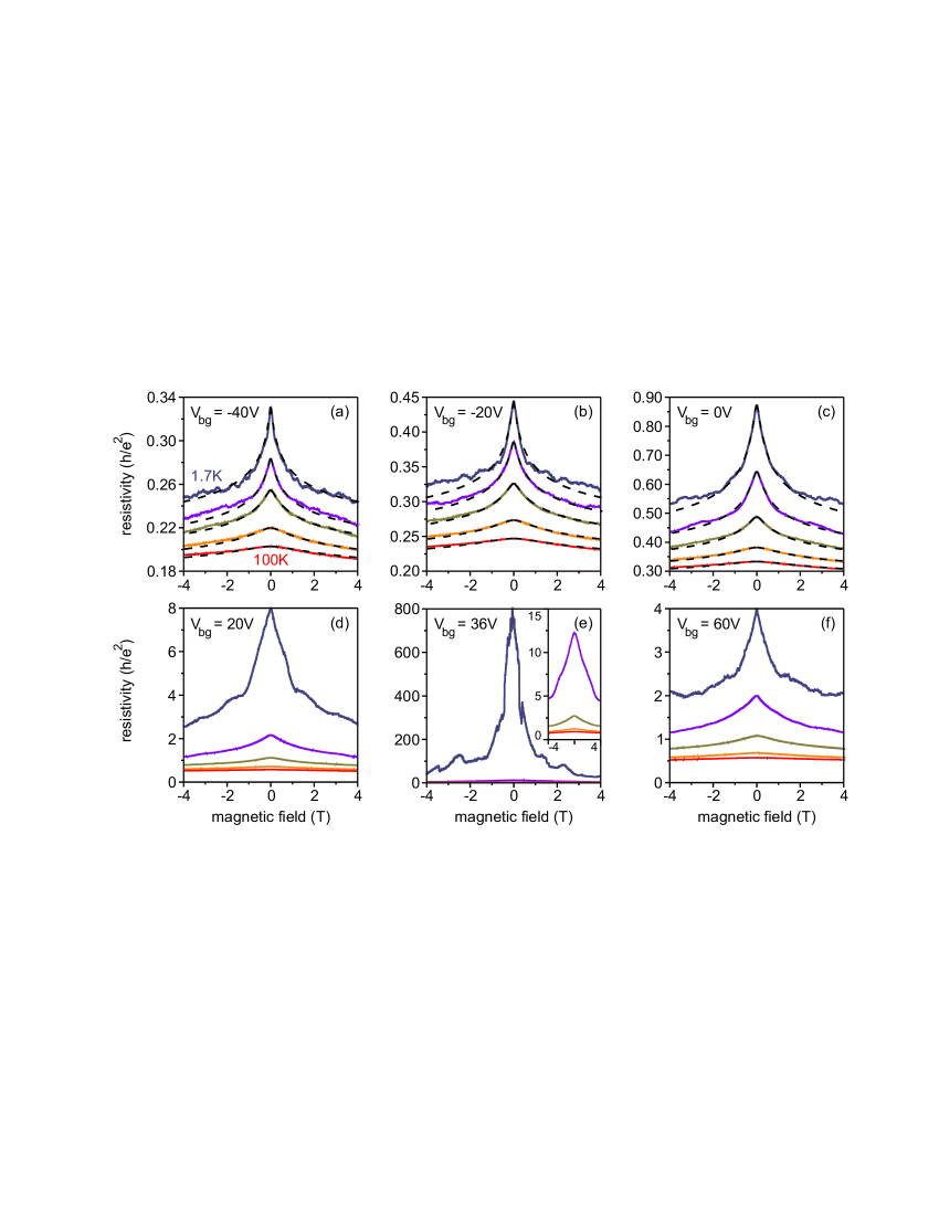
To reveal the contributions of quantum interferences, we explore the transport properties in the presence of a magnetic field (Fig. 4a-f). In all cases, the magnetoresistance is negative, and the resistivity changes with by an amount that strongly depends on . This change becomes increasingly large as the density approaches the Dirac point (, Fig. 4e) whereas it remains moderate at high charge density (, Fig. 4a).
III Discussion
Both the low temperature insulating behavior Aleiner ; Mirlin and the sharp D peak in Raman spectra show that the ozone treatment introduces significant intervalley scattering. A way to quantitatively compare intervalley and intravalley scattering rates is to examine the dependence of the conductivity. Assuming only weak point disorder and charged impurity disorder, we obtain that the intervalley and the intravalley scattering times are comparable, about 10 fs for . Conversely, before ozone treatment the intervalley scattering time is 300 fs and the intravalley scattering time is 100 fs at the same . To determine these scattering times, we consider weak point disorder for the intervalley scattering time and charged-impurity disorder for the intravalley scattering time . The conductivity [due to short range scattering] and the mobility can be extracted from the measurement taken at 100 K (assuming that localization effects are vanishingly small at higher temperature) using Fuhrer_PRL08 . We get and for the pristine graphene, and and after ozone treatment. We note that lattice defects resulting in midgap states were recently identified as a new source of intervalley scattering Fuhrer_PRL09 . The latter scattering results in a linear dependence of so its contribution to the conductivity cannot be discriminated from the one of charged-impurity disorder in a measurement. As such, it can modify and and the intervalley scattering time of 10 fsec is an upper bound.
The magnetoresistance measurements at high can be well described by the weak localization (WL) theory developed for graphene McCann_PRL06 . The correction to the semi-classical (Drude) conductivity reads
| (1) | |||
with where is the digamma function, , and the phase coherence time. To compare with the experiment, we let the diffusion constant and consider only weak point disorder for intervalley scattering and charged-impurity disorder for intravalley scattering. Accordingly, the phase coherence time is the only fitting parameter necessary. As illustrated in Fig. 4(a,b,c) (where ), we find a good agreement between experiments and theory. A satisfactory agreement is also obtained by comparing measurements to WL predictions for conventional two-dimensional metals, which, moreover, yields the same phase coherence time. As for the magnetoresistance measurements at lower (Fig. 4(d,e,f)), the resistivity can change with by a large amount. Comparing the measurements to theory is however difficult at this stage. More measurements at low temperature will be needed to discern among the various predicted dependencies xiB .
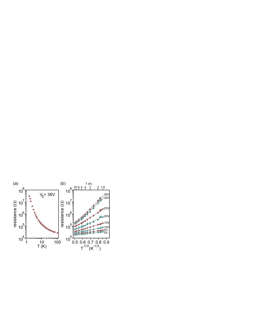
We now turn our attention to the temperature dependence of the resistance. The resistance at the Dirac point diverges at low temperature, as expected for an insulating regime (Fig. 5a). Fig. 5b shows that the temperature-dependent resistance is consistent with two-dimensional variable-range hopping, . Even though the measurement could also be described by a simple thermal activation behavior, for the time being we will restrict our analysis to a variable range hopping scenario, which is the conventional mechanism to describe low temperature conduction in strongly disordered materials Geim_Science09 ; Gomez-Navarro_NL07 ; Kaiser_NL09 ; Efros . This allows us to extract the localization length from the fitting parameter Efros :
| (2) |
where is the density of states of graphene. To estimate , we assume that to take the fluctuations of the Dirac point with respect to the Fermi energy into account Amelia_PRL . Here, F/m2 is the backgate capacitance Amelia_PRL . Letting (which roughly accounts for the smoothing of the vs curve around the Dirac point at the highest temperature), we obtain at the Dirac point. Away from the Dirac point, we find that increases upon increasing (Fig. 6a). As a comparison, we can evaluate the localization length using the rough estimate Gershenson_PRL :
| (3) |
The elastic length is derived from the Drude conductivity as , assuming that is the conductivity measured at a temperature of 100 K. This yields at the Dirac point, which is close to the variable range hopping estimate. The agreement is also quite reasonable at higher (Fig. 6a). Overall, this rough agreement gives us confidence in the order of magnitude of the localization length.
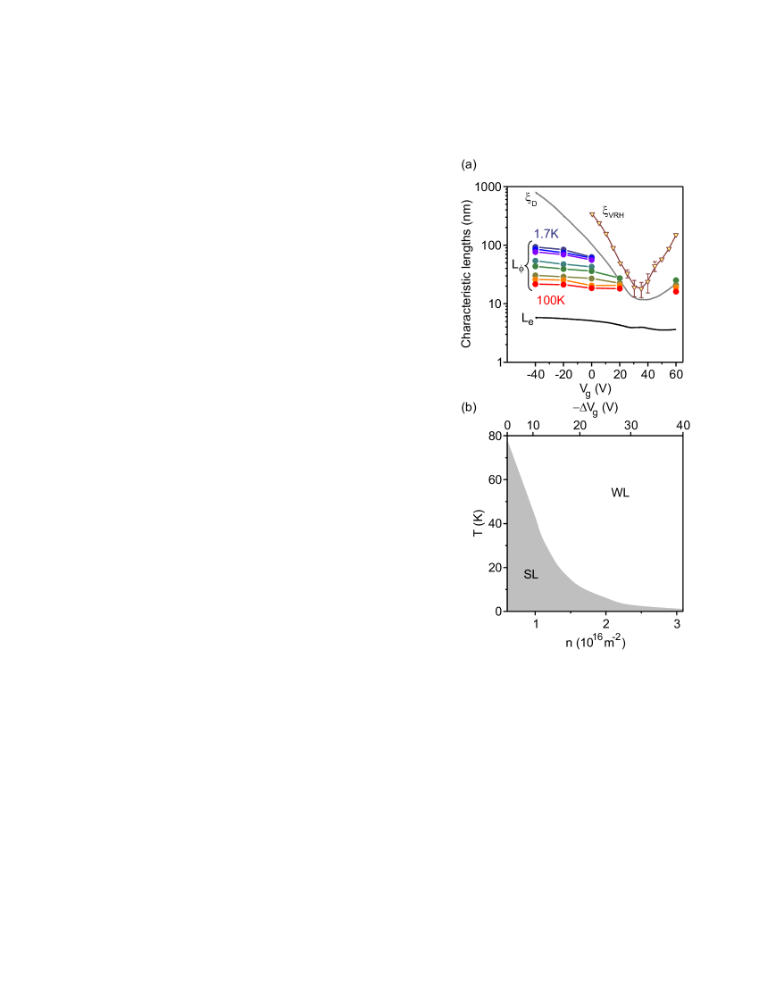
The transition from weak localization to strong localization can be understood by contrasting the fundamental transport length scales extracted from our experimental data (Fig. 6a). As long as the phase coherence length remains smaller than the estimated localization length , the weak localization regime prevails. Whenever becomes comparable to , we observe that the conductivity is close to , the value at which the transition to strong localization is expected Lee_RMP85 . Fig. 6a displays only when at zero magnetic field (and except at the Dirac point). In the opposite case , the comparison between experiment and weak-localization theory becomes worse, so that extracting a value for is meaningless.
Graphene offers the possibility to tune the carrier density with , which provides a practical knob to test the localization theory. From our measurements, we can construct a ”phase diagram” of the transition from weak (WL) to strong localization (SL) as a function of and temperature (Fig. 6b). To do this, we use the temperature dependence of (a few such curves are shown in Fig. 3(b)) and define the transition as . We emphasize that the transition is expected to be gradual and to develop as a smooth crossover Lee_RMP85 . Figure 6b shows that the WL-SL transition is very sensitive to at low carrier concentration. This is because of the strong variation of upon varying (Fig. 6a). By contrast, the other fundamental transport lengths, and , remain essentially constant.
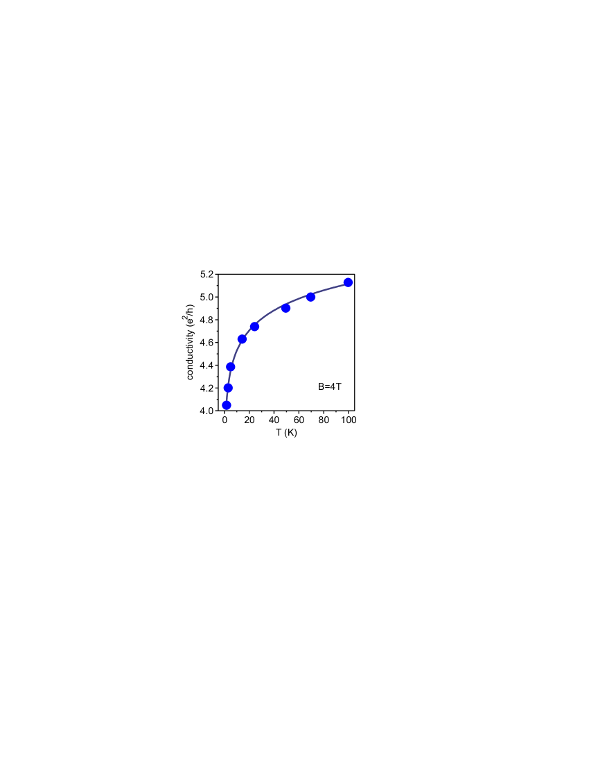
Eventually, one interesting outcome of our measurements is that they reveal the importance of Coulomb interaction between charge carriers. This can be seen in the magnetoresistance measurements at high magnetic field (Fig. 4a) where the conductivity at is definitely temperature dependent. The contribution of weak localization is reduced at high magnetic field and the remaining correction to is usually attributed to Coulomb interaction. The correction to the conductivity due to Coulomb interaction in a two-dimensional metal reads Beenakker ; AAL
| (4) |
where is a constant of the order of unity. Figure 7 shows that experiment agrees well with the theory using . Unlike weak localization, which originates from a change in the diffusion constant Beenakker , this Coulomb interaction effect is a correction to the density of states. These results indicate that the correction to the conductivity due to Coulomb interaction cannot be neglected in the transition between weak localization and strong localization in graphene, as it is treated in existing theoretical works Suzuura_Ando_JPSJ ; Altland ; Aleiner ; Nomura ; Mirlin ; Robinson ; Roche_PRL ; Morpurgo ; McCann_PRL06 .
IV Conclusion
We have reported on the crossover from weak localization to strong localization in disordered graphene, the disorder being created with ozone. For this, we have carried out magneto-transport measurements as a function of gate voltage and temperature. We have shown that the transition between weak and strong localization occurs as the phase coherence length becomes comparable to the localization length and that the transition is very sensitive to the charge carrier concentration. In addition, we have demonstrated the importance of the resistivity correction due to disorder-induced electron-electron interaction.
Previous works showed that disorder in graphene obtained by hydrogenation or oxidation can open an energy gap Geim_Science09 ; Gomez-Navarro_NL07 ; Kaiser_NL09 . By contrast, recent calculations reported that this is not the case for graphene exposed to ozone nicolas . In addition, even if such a gap was created, our measurements suggest that it would be very small. Indeed, we obtain an energy gap of 1 meV when we compare the temperature dependence of the resistivity at the Dirac point to a thermal activation behavior. This low value suggests that a gap, if it exists, would be relevant only to measurements near the Dirac point (in our case, it would be included in the interpretation of the measurements at V). Further experimental work is needed to demonstrate whether this energy gap exists or not, using e.g. scanning tunneling microscopy techniques.
V Acknowledgements
We are grateful to M. Lira-Cantu for the use of the ozone chamber
and acknowledge fruitful discussion with F. Guinea. This work was
supported by a EURYI grant, the EU grant FP6-IST-021285-2, and the
MICINN grants FIS2008-06830 and FIS2009-10150. S. R. acknowledges
the ANR/P3N2009 (NANOSIM-GRAPHENE project number
ANR-09-NANO-016-01).
References
- (1) E. McCann, Physics 2, 98 (2009).
- (2) H. Suzuura, and T. Ando, Phys. Rev. Lett. 89, 266603 (2002).
- (3) I. L. Aleiner and K. B. Efetov, Phys. Rev. Lett. 97, 236801 (2006).
- (4) A. Altland, Phys. Rev. Lett. 97, 236802 (2006).
- (5) P. M. Ostrovsky, I. V. Gornyi, and A. D. Mirlin, Phys. Rev. B 74, 235443 (2006).
- (6) E. McCann, K. Kechedzhi, V. I. Fal’ko, H. Suzuura, T. Ando, and B. L. Altshuler, Phys. Rev. Lett. 97, 146805 (2006).
- (7) A. F. Morpurgo and F. Guinea, Phys. Rev. Lett. 97, 196804 (2006).
- (8) S. V. Morozov, K. S. Novoselov, M. I. Katsnelson, F. Schedin, L. A. Ponomarenko, D. Jiang, and A. K. Geim, Phys. Rev. Lett. 97, 016801 (2006).
- (9) X. Wu, X. Li, Z. Song, C. Berger, and W. A. de Heer, Phys. Rev. Lett. 98, 136801 (2007).
- (10) F. V. Tikhonenko, D. W. Horsell, R. V. Gorbachev, and A. K. Savchenko, Phys. Rev. Lett. 100, 056802 (2008).
- (11) F. V. Tikhonenko, A. A. Kozikov, A. K. Savchenko, and R. V. Gorbachev, Phys. Rev. Lett. 103, 226801 (2009).
- (12) Y.-F. Chen, M.-H. Bae, C. C., T. Dirks, A. Bezryadin, and N. Mason, arXiv:0910.3737.
- (13) T. Ando, J. Phys. Soc. Jpn. 75, 074716 (2006).
- (14) E. H. Hwang, S. Adam, and S. Das Sarma, Phys. Rev. Lett. 98, 186806 (2007).
- (15) T. Stauber, N. M. R. Peres, and F. Guinea, Phys. Rev. B 76, 205423 (2007).
- (16) J.-H. Chen, W. G. Cullen, C. Jang, M. S. Fuhrer, and E. D. Williams, Phys. Rev. Lett. 102, 236805 (2009).
- (17) D. C. Elias, R. R. Nair, T. M. G. Mohiuddin, S. V. Morozov, P. Blake, M. P. Halsall, A. C. Ferrari, D. W. Boukhvalov, M. I. Katsnelson, A. K. Geim, and K. S. Novoselov, Science 323, 610 (2009).
- (18) C. Gómez-Navarro, R. T. Weitz, A. M. Bittner, M. Scolari, A. Mews, M. Burghard, and K. Kern, Nano Lett. 7, 3499 (2007).
- (19) A. B. Kaiser, C. Gómez-Navarro, R. S. Sundaram, M. Burghard, and K. Kern, Nano Lett. 9, 1787 (2009).
- (20) A. Bostwick, J. L. McChesney, K. V. Emtsev, T. Seyller, K. Horn, S. D. Kevan, and E. Rotenberg, Phys. Rev. Lett. 103, 056404 (2009).
- (21) C. W. J. Beenakker and H. van Houten, Quantum transport in semiconducting nanostructures, Solid State Physics 44, 1 (1991).
- (22) J. Moser, A. Barreiro, and A. Bachtold, Appl. Phys. Lett. 91, 163513 (2007).
- (23) A. C. Ferrari, J. C. Meyer, V. Scardaci, C. Casiraghi, M. Lazzeri, F. Mauri, S. Piscanec, D. Jiang, K. S. Novoselov, S. Roth, and A. K. Geim, Phys. Rev. Lett. 97, 187401 (2006).
- (24) G. Lee, B. Lee, J. Kim, and K. Cho, J. Phys. Chem. C 113, 14225-14229 (2009).
- (25) C. Jang, S. Adam, J.-H. Chen, E. D. Williams, S. Das Sarma, and M. S. Fuhrer Phys. Rev. Lett. 101, 146805 (2008).
- (26) D. Yoshioka, Y. Ono, H. Fukuyama, J. Phys. Soc. Jpn. 50, 3419 (1981). V. L. Nguyen, B. Z. Spivak, and B. I. Shklovskii, Sov. Phys. JETP 62, 1021 (1985). Y. Ono, Prog. Theor. Phys. Supp. 84 138 (1985). U. Sivan, O. Entin-Wohlman, Y. Imry, Phys. Rev. Lett. 60, 1566 (1988). O. Entin-Wohlman, Y. Imry, U. Sivan, Phys. Rev. B 40, 8342 (1989). B.I. Shklovskii and B.Z. Spivak, in Hopping Transport in Solids, edited by M. Pollak and B.I. Shklovskii (Elsevier, New York, 1991). H. L. Zhao, B. Z. Spivak, M. P. Gelfand, S. Feng, Phys. Rev. B 44, 10760 (1991). P. Kleinert and V. V. Bryksin, Phys. Rev. B 55, 1469 (1997).
- (27) B. I. Shklovskii and A. L. Efros, Electronic properties of doped semiconductors (Springer-Verlag, Berlin, 1984).
- (28) A. Barreiro, M. Lazzeri, J. Moser, F. Mauri, and A. Bachtold, Phys. Rev. Lett. 103, 076601 (2009).
- (29) M. E. Gershenson, Y. B. Khavin, A. G. Mikhalchuk, H. M. Bozler, and A. L. Bogdanov, Phys. Rev. Lett. 79, 725 (1997).
- (30) P. A. Lee and T. V. Ramakrishnan, Rev. Mod. Phys. 57, 287 (1985).
- (31) B. L. Altshuler, A. G. Aronov, and P. A. Lee, Phys. Rev. Lett. 44, 1288 (1980).
- (32) K. Nomura, M. Koshino, and S. Ryu, Phys. Rev. Lett. 99, 146806 (2007). K.-I. Imura, Y. Kuramoto, and K. Nomura, Europhys. Lett. 89, 17009 (2010).
- (33) J. P. Robinson, H. Schomerus, L. Oroszlány, and V. I. Fal’ko, Phys. Rev. Lett. 101, 196803 (2008).
- (34) A. Lherbier, B. Biel, Y.-M. Niquet, and S. Roche, Phys. Rev. Lett. 100, 036803 (2008). A. Cresti, N. Nemec, B. Biel, Y.-M. Niquet, and S. Roche, NanoResearch 1, 361 (2008).
- (35) N. Leconte, J. Moser, P. Ordejon, H. Tao, A. Lherbier, A. Bachtold, F. Alsina, C. M. Sotomayor-Torres, J.-C. Charlier, and S. Roche, submitted.