Nanostructures made from superconducting boron doped diamond
Abstract
We report on the transport properties of nanostructures made from boron-doped superconducting diamond. Starting from nanocrystalline superconducting boron-doped diamond thin films, grown by Chemical Vapor Deposition, we pattern by electron-beam lithography devices with dimensions in the nanometer range. We show that even for such small devices, the superconducting properties of the material are well preserved: for wires of width less than , we measure critical temperatures in the Kelvin range and critical field in the Tesla range.
pacs:
73.23.-b, 75.20.Hr, 72.70.+m, 73.20.Fz1 Introduction
The discovery of superconductivity[1] in has generated a lot of interest for a special class of superconducting materials belonging to the covalent metals. In this context, the observation of superconductivity in highly-doped boron diamond[2] paved the way to the study of superhard superconducting materials[3, 4]. Apart from the fundamental point of understanding of the physical mechanisms leading to the superconductivity in these systems, their interest lies in a very high Young’s modulus, which makes them promising candidates for the fabrication of superconducting Nano Electro-Mechanical Systems of exceptional quality factor. Evidences that both the superconductivity[5, 6, 7] and the mechanical properties[8] are essentially preserved in nanocrystalline layers grown on non-diamond substrates such as silicon have to be checked in order to bring further credit to this approach.
Most of the studies, however, have so far focused on the properties of bulk superconducting diamond, and it still remains to be shown what happens when the material is patterned into nanostructures. In this paper, we present a comprehensive study of nanostructured superconducting polycrystalline diamond films. Our measurements show that the critical temperature of the nanostructures being 2.5 K while for the bulk this is 3.5 K. The critical field for these structures is approximately mT at 50mK.
2 Experimental
The nanocrystalline boron-doped diamond was obtained by Chemical Vapour Deposition on a silicon oxide wafer. Prior to growth, wafers were cleaned with () solution at for , and rinsed in pure DI water in an ultrasonic bath. In order to enhance nucleation, wafers were then seeded with diamond nano-particles from an aqueous colloid of mono-disperse diamond particles known to have sizes less than in solution as confirmed by dynamic light scattering[9, 10]. Atomic Force Microscope (afm) measurements have shown this technique to result in uniform nucleation densities far in excess of . Diamond growth was then performed by microwave plasma enhanced chemical vapour deposition (mpcvd) from diluted in with additional boron from a trimethylboron gas source. The microwave power was at , the substrate temperature being around as monitored in situ with a bichromatic pyrometer.

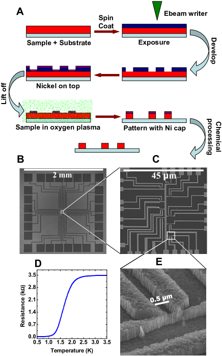
Nanostructured devices have then been fabricated from this material. In figure 1 we present a diagram of the entire nanofabrication process. The wafer was first spin-coated with polymethyl-methacrylate (pmma) to form a thick layer and prebaked at for . The next step was the exposure to the electron beam with a dose of for an acceleration voltage of . After exposure, the pattern was developed in solution of methyl isobutyl ketone (mibk) and iso-propyl alcohol (ipa) for . A thin layer of nickel () has then been deposited and patterned using a standard electron-gun evaporator and lift-off technique. This layer acts as a mask for the plasma etching of the diamond structures subsequently done using Electron Cyclotron Resonance oxygen plasma[11] and a bias for . This leads to an etching rate of . This mask was finally removed using an solution. Ohmic contacts were then obtained by an evaporation of metals ().
Panel B, C and E of figure 1 show sem pictures of the obtained nanostructures, namely wires of different widths and lengths. Panel E represents the smallest device we have been able to fabricate, a wire of length and width ; note that in this case the aspect ratio is as high as , the anisotropy of the plasma etching allowing to pattern one single grain. The superconducting transition of this wire is presented in panel D showing a critical temperature of K. Panel B in figure 1 shows a typical microcircuit used for our measurements and panel C is the blow-up of a area in the center of the microcircuit.
3 Results and Discussion

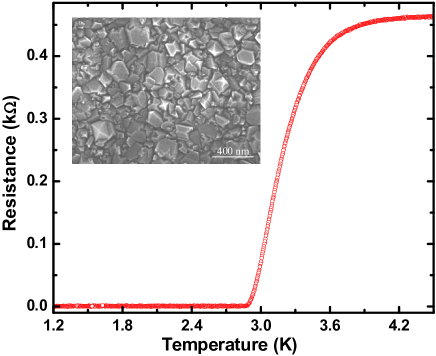
A Scanning Electron Microscope (sem) picture (inset of figure 2) of the sample shows grains of typical size for a film thickness of , consistent with the nucleation density. Four silver paste electrical contacts, about apart from each other, have been deposited at the surface for the characterisation of the as-grown layer. The 4-points resistance was measured as a function of temperature using these contacts and a standard lock-in technique under a very low current injection of . Typical data are presented in figure 2: a clear superconducting transition is observed with a zero resistance at . The width of the transition is quite large, typically with a of the onset resistance criterion; we attribute this width to the distribution of the sizes of the grains in the material.


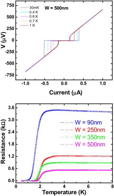
Electrical characterisation of the devices were performed in both a and a dilution refrigerators. Bottom panel of figure 3 shows the critical temperature of wires of various widths, measured with very low current (typically ); no significant difference was observed from the critical temperature measured on the “bulk” sample ( for this wafer) except for the case of the narrowest wire (below wide, ). This is a generic observation for all our samples: the critical temperature of our wires is those of the bulk material except for wires thinner than typically ; in this case, it is slightly reduced. Figure 3 shows the voltage-current () characteristic of a wide wire measured at different temperatures[12]. The curves are hysteretic due to thermal effect: when the critical current is reached, Joule effect heats up the wire and the critical current measured when subsequently decreasing the current is thus much lower than the critical current measured when increasing the current[13, 14]; moreover, this “retrapping” current is independent of the temperature of the refrigerator, as the actual temperature of the sample is then fixed by the current trough the wire.
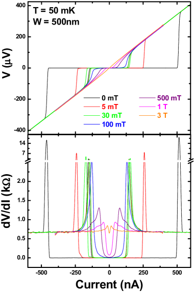
Critical field measurements were performed by applying a magnetic field perpendicular to the structure. characteristics for a wide wire under different magnetic fields and at are presented on the top panel of figure 4. As expected, the critical current decreases when applying a magnetic field. It should be stressed that for magnetic fields larger than , the characteristic is not hysteretic: in this case, the Joule heating becomes negligible as the critical current is strongly lowered, and both (“increasing” and “decreasing”) critical currents become similar. In order to get more insights on the superconductivity of our devices under magnetic field, we have numerically calculated the derivatives of the characteristics: the obtained curves are displayed on the bottom panel of figure 4. For magnetic fields smaller than , a clear zero is observed around , as expected for a superconductor. More interestingly, we observe a dip at zero current in the characteristic for magnetic fields above . This demonstrates that one can still observe traces of superconductivity above 3T in our nanometric wires, the most probable mechanism being that some grains remain superconducting under very high magnetic fields. More local studies, such as Scanning Tunneling Spectroscopy measurements[15, 16], are certainly desirable to fully understand the robustness of the superconductivity observed in our system.
4 Conclusion
In conclusion, we have successfully fabricated nanostructures from boron-doped nanocrystalline superconducting diamond. Using electron beam lithography, we have fabricated devices of characteristic size less that and aspect ratio as high as . These structures have critical temperatures in the Kelvin range, similar to what is observed in “bulk” films; typical bulk Tc being 3.5K while for nanostructures it is 2.5K except for 90nm wire where it is 1K. We measure critical fields close to and traces of superconductivity are observed above . This study proves that superconductivity in boron-doped diamond is a very robust phenomenon which makes it a promising candidate for future applications in the field of superconducting Nano Electro-Mechanical Systems.
Refrences
References
- [1] J. Nagamatsu, N. Nakagawa, T. Muranaka, Y. Zenitani and J. Akimitsu, Nature 410, 63 (2001).
- [2] E. A. Ekimov, V. A. Sidorov, E. D. Bauer, N. N. Mel’nik, N. J. Curro, J. D. Thompson and S. M. Stishov, Nature 428, 542 (2004).
- [3] X. Blase , É. Bustarret , C. Chapelier , T. Klein and C. Marcenat, Nature Materials 8, 375 (2009).
- [4] G. A. Dubitskiy, V. D. Blank, S. G. Buga, E. E. Semenova, V. A. Kul bachinskii, A. V. Krechetov and V. G. Kytin, JETP Lett. 81, 260 (2005)
- [5] M. Nesládek, D. Tromson, C. Mer, P. Bergonzo, P. Hubik and J. J. Mares, Appl. Phys. Lett. 88, 234111 (2006).
- [6] W. Gajewski, P. Achatz, O. A. Williams, K. Haenen, È. Bustarret, M. Stutzmann and J. A. Garrido, Phys. Rev. B 79, 045206 (2009).
- [7] P. Achatz, W. Gajewski, É. Bustarret, C. Marcenat, R. Piquerel, C. Chapelier, T. Dubouchet, O. A. Williams, K. Haenen, J. A. Garrido and M. Stutzmann, Phys. Rev. B 79, 201203 (2009).
- [8] M. Imboden, P. Mohanty, A. Gaidarzhy, J. Rankin and B. W. Sheldon, Appl. Phys. Lett. 90, 173502 (2007).
- [9] O. A. Williams, O. Douhéret, M. Daenen, K. Haenen, E. Ōsawa and M. Takahashi, Chem. Phys. Lett. 445, 255 (2007).
- [10] M. P. Villar, M. P. Alegre, D. Araujo, É. Bustarret, P. Achatz, L. Saminadayar, C. Bäuerle and O. A. Williams, Phys. Stat. Sol. (a) 206, 1986 (2009).
- [11] M. Bernard, A. Deneuville, T. Lagarde, É. Treboux, J. Pelletier, P. Muret, N. Casanova and É. Gheeraert, Diamond and Related Materials 11, 828 (2002).
- [12] The asymmetry seen in the VI characteristics mainly arises due to an offset in our experimental setup, however, there is also a residual asymmetry which is presently not understood.
- [13] W. Rabaud, L. Saminadayar, D. Mailly, K. Hasselbach, A. Benoît and B. Étienne, Phys. Rev. Lett. 86, 3124 (2001).
- [14] H. Courtois, M. Meschke, J. T. Peltonen and J. P. Pekola, Phys. Rev. Lett. 101, 067002 (2008).
- [15] B. Sacépé, C. Chapelier, C. Marcenat, J. Kac̆marc̆ik, T. Klein, M. Bernard and É. Bustarret, Phys. Rev. Lett. 96, 097006 (2006).
- [16] F. Dahlem, P. Achatz, O. A. Williams, D. Araujo, É. Bustarret and H. Courtois, arXiv: Cond-Mat 0912.3727v1 (2009).