Fast tunnel rates in Si/SiGe one-electron single and double quantum dots
Abstract
We report the fabrication and measurement of one-electron single and double quantum dots with fast tunnel rates in a Si/SiGe heterostructure. Achieving fast tunnel rates in few-electron dots can be challenging, in part due to the large electron effective mass in Si. Using charge sensing, we identify signatures of tunnel rates in and out of the dot that are fast or slow compared to the measurement rate. Such signatures provide a means to calibrate the absolute electron number and verify single electron occupation. Pulsed gate voltage measurements are used to validate the approach.
The spins of electrons isolated in quantum dots are promising candidates for solid-state qubits.Loss and Divincenzo (1998) Spin readout and manipulation have been demonstrated in GaAs quantum dots, using both one and two-electron spin states as logical qubits.Elzerman et al. (2004); Petta et al. (2005); Koppens et al. (2006) To enable successful error correction, it is advantageous to have spin dephasing times and lifetimes as long as possible. Because isotopes of Si with zero nuclear spin exist, resulting in particularly slow electron spin dephasing and long lifetimes,Tahan et al. (2002); Tyryshkin et al. (2003); de Sousa and Das Sarma (2003) a number of proposals have been made to construct spin qubits based on confined electrons in Si quantum dots and donors.Kane (1998); Vrijen et al. (2000); Friesen et al. (2003); Hollenberg et al. (2006); Morello et al. (2009) There has been significant progress in the development of quantum dots in Si,Slinker et al. (2005); Berer et al. (2006); Angus et al. (2007); Hu et al. (2007); Zimmerman et al. (2007); Shaji et al. (2008); Liu et al. (2008); Lansbergen et al. (2008); Fuhrer et al. (2009); Simmons et al. (2009); Nordberg et al. (2009); Hayes et al. (2009); Xiao et al. (2009) but achieving single-charge occupation in Si dots is challenging. One issue is the relatively large electron effective mass in Si, which leads to smaller tunnel rates than would arise for the same size and shape barrier in materials with lighter m∗. While occupation of Si single quantum dots by individual charges has been demonstrated for both electron Simmons et al. (2007); Lim et al. (2009) and hole Zwanenburg et al. (2009) dots, a double quantum dot with a single electron in each dot, the foundation for coupled qubits, or the two-electron singlet-triplet qubit,Taylor et al. (2005) has not been achieved until now.
This letter reports the demonstration of Si/SiGe single and double quantum dots occupied by zero, one, and two electrons, and it describes signatures of fast tunnel rates in the one-electron limit for these dots. We show that tunnel rates in Si/SiGe quantum dots change noticeably over moderate gate voltage ranges that correspond to removing several electrons from the quantum dot. This change is rapid enough to require retuning of the tunnel barriers in and out of the dot when approaching the one-electron state. By careful tuning of the gate voltages, we can measure reliably the expulsion of the last electron from the quantum dot, providing an absolute reference for charge counting. By using pulsed gate voltages in combination with charge sensing, we demonstrate electron tunneling at rates as high as in a one-electron single quantum dot and in a one-electron double quantum dot.

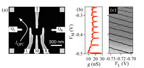
The quantum dot used in this work is formed in a Si/SiGe heterostructure containing a two-dimensional electron gas approximately 79 nm below the crystal surface, with a carrier density of and mobility of , after illumination with red light for while at a temperature of at the beginning of the experiment. The heterostructure consists of an undoped relaxed buffer of Si/Si0.71Ge0.29, a strained-Si quantum well thick, undoped Si/Si0.71Ge0.29, phosphrous-doped Si/Si0.71Ge0.29, undoped Si/Si0.71Ge0.29, and a Si cap layer. Fig. 1(a) shows a scanning electron micrograph of a device with the same gate structure as that reported here. The top-gates are formed by electron-beam evaporation of Pd onto the HF-etched surface of the heterostructure, following a gate design similar to Ref. Ciorga et al. (2000). The gates sit on a square mesa of width that was defined by reactive ion etching. The squares at the four corners represent the directions toward available ohmic contacts. All measurements reported below were performed in a dilution refrigerator with a mixing chamber temperature below .
The quantum dot is formed by the application of negative voltages to gates , , and . The dot is tuned to the few-electron regime by making the voltages on the gates more negative. Two charge sensing point contacts are formed by the application of negative voltage to the left () and right () quantum point contact (QPC) gates; only the data from the left point contact is presented here. Fig. 1(b) is a plot of the transconductance as a function of , where is the current through the point contact. The regularly spaced peaks in represent changes in the charge occupation of the dot of one electron. Fig. 1(c) shows as a function of and ; the peaks in lie along straight lines, indicating that the device is a single quantum dot in this gate voltage regime.
A key question is how to assess when the last observable line in a plot such as that shown in Fig. 1(c) represents the removal of the last electron in the quantum dot. One typically expects the changes in gate voltage to become non-uniform as the last electron is approached.Simmons et al. (2007) A concern that is sometimes raised is whether the tunnel rate into the dot has become sufficiently slow that an additional transition is simply missed. This concern is perhaps especially well taken in Si, because the effective mass of electrons in silicon () is higher than that in GaAs (), the most widely studied host for semiconductor quantum dots. Because of its relatively large , tunnel rates in Si will vary much more strongly as the tunnel barrier is changed than in GaAs. As a result, care must be taken, in device design and in experimental measurements, to ensure that the tunnel barriers do not turn opaque as gate voltages are made more negative and the few electron regime is reached. We show that such changes in tunnel rates yield clear signatures in the data, enabling the device used here to be reliably tuned to a regime with fast tunnel rates.

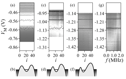
Fig. 2 shows signatures of both fast and slow tunnel rates. The gray-scale reports versus for repeated sweeps of through the same voltage range. For these sweeps, the dwell time per data point is , and the voltage step per data point is in (a) & (c) and in (e) & (g). The horizontal axis is an index representing the sweep number. Near the top of Fig. 2a, the gray lines corresponding to charge transitions are straight and smooth: electrons hop out of the dot as soon as the dot chemical potential crosses the Fermi level of the leads, and the tunneling time is small compared with the dwell time per data point. As is made more negative, the number of electrons in the dot decreases, and at the same time cross-talk between gate and the quantum dot entrance and exit point contacts reduces the tunnel coupling between the dot and the leads, increasing . Eventually approaches and then exceeds the dwell time per data point, and near the bottom of panel (a) the horizontal lines are no longer smooth but rather exhibit random fluctuations. An important feature of the data in Fig. 2 is that the breaking up of the charge transition lines is gradual: in Fig. 2(a), the line at is smooth and straight, and the next two lines, while clearly in the limit of slow , are nonetheless easily discernible. Fig. 2(b) shows a schematic representation of the potential landscape of the dot for the conditions of panel (a).
Fig. 2(c) & (d) show plots analogous to (a) & (b), with the voltages and changed to increase the coupling to the left lead at the expense of that to the right lead. Because the tunnel couplings act in parallel, such a procedure reduces the tunneling time , and one expects to see smoother horizontal lines. In Fig. 2(c), the vertical axis is offset to correct for the effect of changing and , lining up the same charge transitions in (a) and (c). The second to last charge transition is now straight and smooth, indicating a faster tunnel rate than in (a), while the last transition is still uneven. Note that the sensitivity of the charge-sensing point contact to electron tunneling events is also improved in (c) compared with (a), because the changes in gate voltage shift the position of the dot to the left, closer to the charge sensing channel. Fig. 2(e) & (f) show the results of repeating this procedure; again, identical charge transitions are aligned. All of the lines are now straight and smooth, no additional lines have appeared below the final transition, and the sensitivity of the charge sensing is higher still.
The conditions in Fig. 2(e) now correspond to tunnel rates fast enough that relatively high-frequency pulsed-gate voltage measurements can be performed. Fig. 2(g) shows the time-average of the conductance in the presence of a square wave pulse of constant peak-to-peak amplitude applied to , in addition to its dc voltage. In Fig. 2(g), every transition line has split into two lines with no change in intensity as a function of frequency for frequencies up to , indicating that the loading and unloading rates of electrons into and out of the dot are faster than the pulse frequency over this entire frequency range.

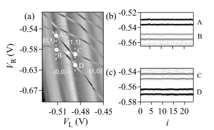
We now reconfigure the voltages on the gates and move smoothly from the one-electron single dot regime to the one-electron double dot regime. To split the single dot into a double dot, is made more negative, and the other gate voltages are adjusted to keep the one electron line visible during this procedure. Fig. 3 (a) is a plot of as a function of and in the double dot regime, showing the characteristic “honeycomb” charge transition lines expected for a double dot. The extended empty region toward the lower left corner corresponds to the (0,0) charge configuration. We characterize the tunnel rates of the and transitions by applying voltage pulses to gate . Fig. 3(b) shows as a function of the sweep index and , with a square-wave pulse of peak-to-peak amplitude added to . The white dashed-line in Fig. 3(a) represents the sweep taken in for this measurement. The charge transition lines, corresponding to the letters A and B in Fig. 3(a), split into two smooth lines in Fig. 3(b), demonstrating that the tunnel rates to access each of these charge states are at least of the order of , and that the tunneling times are much faster than the dwell time per data pixel in Fig. 3(a), which is . Fig. 3(c) shows a similar measurement at the locations of points C and D. Note that the data in 3(a) and that in (b) & (c) were taken on different days, explaining the small shift in the operating point between the two sets of data.
We have presented charge sensing data for single and double Si/SiGe quantum dots in the one-electron regime. We find that tuning the gate voltages provides good control over the tunnel rates in this regime, and that pulsed gate voltage measurements can be performed on both single and double dots. For the single dot, one tunnel barrier can be made fast by allowing the other tunnel barrier to become slow. Here we have demonstrated tunnel rates in excess of using this approach. We have also shown that fast tunnel rates can be achieved in a symmetric double-dot regime, in which both dots are well-coupled to their corresponding lead. We have demonstrated tunnel rates in excess of to each of those leads. Further increases in tunnel rates are likely to be achievable for the symmetric operating regime by changing the size of the lithographic gate pattern.
This work was supported in part by ARO and LPS (W911NF-08-1-0482), by NSF (DMR-0805045), by United States Department of Defense, and by DOE (DE-FG02-03ER46028). The views and conclusions contained in this document are those of the authors and should not be interpreted as representing the official policies, either expressly or implied, of the U.S. Government. This research utilized NSF-supported shared facilities at the University of Wisconsin-Madison.
References
- Loss and Divincenzo (1998) D. Loss and D. P. Divincenzo, Phys Rev A 57, 120 (1998).
- Elzerman et al. (2004) J. M. Elzerman, R. Hanson, L. H. W. van Beveren, B. Witkamp, L. M. K. Vandersypen, and L. P. Kouwenhoven, Nature 430, 431 (2004).
- Petta et al. (2005) J. R. Petta, A. C. Johnson, J. M. Taylor, E. A. Laird, A. Yacoby, M. D. Lukin, C. M. Marcus, M. P. Hanson, and A. C. Gossard, Science 309, 2180 (2005).
- Koppens et al. (2006) F. H. L. Koppens, C. Buizert, K. J. Tielrooij, I. T. Vink, K. C. Nowack, T. Meunier, L. P. Kouwenhoven, and L. M. K. Vandersypen, Nature 442, 766 (2006).
- Tahan et al. (2002) C. Tahan, M. Friesen, and R. Joynt, Phys Rev B 66, 035314 (2002).
- Tyryshkin et al. (2003) A. M. Tyryshkin, S. A. Lyon, A. V. Astashkin, and A. M. Raitsimring, Phys Rev B 68, 193207 (2003).
- de Sousa and Das Sarma (2003) R. de Sousa and S. Das Sarma, Phys Rev B 68, 115322 (2003).
- Kane (1998) B. E. Kane, Nature 393, 133 (1998).
- Vrijen et al. (2000) R. Vrijen, E. Yablonovitch, K. Wang, H. W. Jiang, A. Balandin, V. Roychowdhury, T. Mor, and D. Divincenzo, Phys. Rev. A 62, 012306 (2000).
- Friesen et al. (2003) M. Friesen, P. Rugheimer, D. E. Savage, M. G. Lagally, D. W. van der Weide, R. Joynt, and M. A. Eriksson, Phys Rev B 67, 121301 (2003).
- Hollenberg et al. (2006) L. C. L. Hollenberg, A. D. Greentree, A. G. Fowler, and C. J. Wellard, Phys Rev B 74, 045311 (2006).
- Morello et al. (2009) A. Morello, C. C. Escott, H. Huebl, L. H. W. van Beveren, L. C. L. Hollenberg, D. N. Jamieson, A. S. Dzurak, and R. G. Clark, Phys Rev B 80, 081307 (2009).
- Slinker et al. (2005) K. A. Slinker, K. L. M. Lewis, C. C. Haselby, S. Goswami, L. J. Klein, J. O. Chu, S. N. Coppersmith, R. Joynt, R. H. Blick, M. Friesen, et al., New J Phys 7, 246 (2005).
- Berer et al. (2006) T. Berer, D. Pachinger, G. Pillwein, M. Mühlberger, H. Lichtenberger, G. Brunthaler, and F. Schäffler, Appl Phys Lett 88, 162112 (2006).
- Angus et al. (2007) S. J. Angus, A. J. Ferguson, A. S. Dzurak, and R. G. Clark, Nano Lett 7, 2051 (2007).
- Hu et al. (2007) Y. Hu, H. O. H. Churchill, D. J. Reilly, J. Xiang, C. M. Lieber, and C. M. Marcus, Nat Nanotechnol 2, 622 (2007).
- Zimmerman et al. (2007) N. M. Zimmerman, B. J. Simonds, A. Fujiwara, Y. Ono, Y. Takahashi, and H. Inokawa, Appl Phys Lett 90, 033507 (2007).
- Shaji et al. (2008) N. Shaji, C. B. Simmons, M. Thalakulam, L. J. Klein, H. Qin, H. Luo, D. E. Savage, M. G. Lagally, A. J. Rimberg, R. Joynt, et al., Nat Phys 4, 540 (2008).
- Liu et al. (2008) H. W. Liu, T. Fujisawa, Y. Ono, H. Inokawa, A. Fujiwara, K. Takashina, and Y. Hirayama, Phys Rev B 77, 073310 (2008).
- Lansbergen et al. (2008) G. P. Lansbergen, R. Rahman, C. J. Wellard, I. Woo, J. Caro, N. Collaert, S. Biesemans, G. Klimeck, L. C. L. Hollenberg, and S. Rogge, Nat Phys 4, 656 (2008).
- Fuhrer et al. (2009) A. Fuhrer, M. Füchsle, T. C. G. Reusch, B. Weber, and M. Y. Simmons, Nano Lett 9, 707 (2009).
- Simmons et al. (2009) C. B. Simmons, M. Thalakulam, B. M. Rosemeyer, B. J. V. Bael, E. K. Sackmann, D. E. Savage, M. G. Lagally, R. Joynt, M. Friesen, S. N. Coppersmith, et al., Nano Lett 9, 3234 (2009).
- Nordberg et al. (2009) E. P. Nordberg, G. A. T. Eyck, H. L. Stalford, R. P. Muller, R. W. Young, K. Eng, L. A. Tracy, K. D. Childs, J. R. Wendt, R. K. Grubbs, et al., Phys Rev B 80, 115331 (2009).
- Hayes et al. (2009) R. R. Hayes, A. A. Kiselev, M. G. Borselli, S. S. Bui, E. T. C. III, P. W. Deelman, B. M. Maune, I. Milosavljevic, J.-S. Moon, R. S. Ross, et al. (2009), arXiv:0908.0173.
- Xiao et al. (2009) M. Xiao, M. G. House, and H. W. Jiang (2009), arXiv:0909.2857v1.
- Simmons et al. (2007) C. B. Simmons, M. Thalakulam, N. Shaji, L. J. Klein, H. Qin, R. H. Blick, D. E. Savage, M. G. Lagally, S. N. Coppersmith, and M. A. Eriksson, Appl Phys Lett 91, 213103 (2007).
- Lim et al. (2009) W. H. Lim, F. A. Zwanenburg, H. Huebl, M. Möttönen, K. W. Chan, A. Morello, and A. S. Dzurak, Appl Phys Lett 95, 242102 (2009).
- Zwanenburg et al. (2009) F. A. Zwanenburg, C. E. W. M. V. Rijmenam, Y. Fang, C. M. Lieber, and L. P. Kouwenhoven, Nano Lett 9, 1071 (2009).
- Taylor et al. (2005) J. Taylor, H. Engel, W. Dur, A. Yacoby, C. Marcus, P. Zoller, and M. Lukin, Nat Phys 1, 177 (2005).
- Ciorga et al. (2000) M. Ciorga, A. S. Sachrajda, P. Hawrylak, C. Gould, P. Zawadzki, S. Jullian, Y. Feng, and Z. Wasilewski, Phys Rev B 61, R16315 (2000).