Hot Electron Terahertz Oscillations in Graphene:
Crater and Terraces in the Carrier Distribution Function.
Abstract
In graphene, after the electric field is turned-on, the ballistic acceleration of charge carriers up to the monochromatic optic phonon energy generates a back-and-forth motion of the whole distribution function between the zero point energy and the phonon energy. This effect is predicted to manifest in damped terahertz oscillations of the carrier drift velocity and average energy. The most dramatic feature of this transient phenomenon is the onset of momentum-free areas surrounded by high momentum probability in phase space, and smooth steps or terraces in the distribution function. This dynamical effect that only takes place within a voltage and sample length window, is the direct consequence of the interplay between the electric force and the randomizing nature of deformation potential optic phonons in the linear band structure of graphene.
keywords:
Hot carriers, graphene, Boltzmann transport, transientBeckman Institute \altaffiliationBeckman Institute Department of Physics] Department of Physics \alsoaffiliation[Department of Electrical and Computer Engineering] Beckman Institute, University of Illinois at Urbana-Champaign, Urbana, Illinois 61801 \abbreviationsIR,NMR,UV
Keywords: Hot carriers, graphene, Boltzmann transport, transient
Since its isolation in monolayer sheets 1, graphene has emerged as a new and ideal two-dimensional (2D) material with exotic electronic properties 2. The particular nature of its band structure with a linear dispersion between energy and momentum , where is the Fermi velocity of electron and holes, results in a zero-gap material, where the overlap between the valence and conduction band is reduced to a single point around the K and K’ symmetry points of the Brillouin zone 2, 3. Hence, charge carrier dynamics can be described by a formalism similar to Dirac relativistic equation, where the speed of light is replaced by which provides new opportunity to observe “quantum electro-dynamic” effects in nanoscale systems. For electronics applications, graphene is similarly attractive because of the linear energy-momentum dispersion, for which all charge carriers move with the velocity, much larger than in conventional semiconductor materials 4, which anticipates faster time response.
Indeed, the carrier mean free path for collisions with low energy acoustic phonons (AP) can reach several micrometers, while efficient scattering with monochromatic optic phonons (OP) occurs at much larger energy 5 than in conventional semiconductors 6. Therefore, in electric fields high enough (to escape AP or low energy scattering), charge carriers can experience quasi-ballistic run-away until they scattered with efficient OP emission once 7. The coherent aspect of this process i.e. the coherent acceleration of the carrier distribution function followed by quasi-instantenous carrier relaxation by OPs at high energy is expected to produce oscillations of the carrier velocity with a periodicity given by 8.
In this paper we investigate carrier dynamics in graphene single layers, once the electric field has been turned-on, to determine the conditions of occurrence of current oscillations. Indeed, the thermal broadening of the initial distribution introduces a decoherence in the OP relaxation amongst carriers, which asides from low energy scattering, causes inherent damping of the oscillations, especially at high fields, where carriers overshoot the OP energy before emission. For this purpose, we use the Boltzmann formalism, and solve for the time-varying carrier distribution in the presence of OP scattering 8, 9, 10. We also account for low energy scattering such as impurities and acoustic phonons, by using the relaxation time approximation. In weak concentrations , electron-electron interactions do not play a major role in transport in graphene 11, and are not included in this analysis. We provide an analysis of the interplay between applied electric fields and strength of the low energy scattering rates for the onset of oscillations.
Model. Let us consider a system of electrons in the graphene conduction band under the influence of an electric field along the x-direction. We divide the momentum space into two regions, I () and II () separated by a circle of critical momentum , that corresponds to the electron kinetic energy equal to (Fig. 1a).
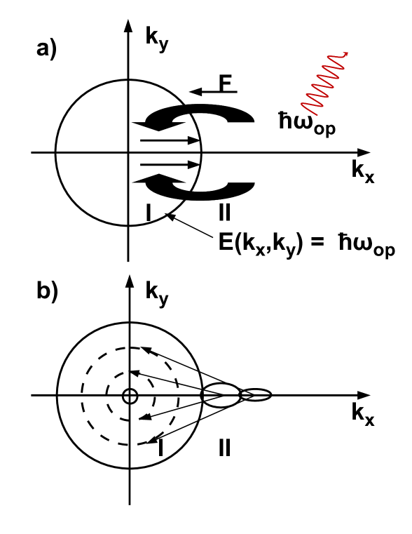
In region I electrons undergo quasi-ballistic acceleration and weak scattering by low energy mechanisms (e.g. impurities or APs) until they reach region II where they lose their energy by OP emission, and scatter back to region I. In our model, the electric field is assumed to be low enough so that electrons are scattered efficiently from region II to region I by OP emission with little probability to reach .
In the two regions, the time-dependent Boltzmann equations read:
| (1a) |
| (1b) |
where and are the time-dependent momentum distribution functions in regions I and II respectively, and is the electric field applied Leburton. The first terms in RHS of equations (1) account for low energy scattering mechanisms where,
| (2) |
is the Fermi-Dirac equilibrium distribution function, and is the relaxation time (for the sake of simplicity, we assume is -independent and we vary it’s value compared to the OP scattering rate). is the OP transition rate from a state with momentum to the state with momentum , given by 12
| (3) |
where is the optical deformation potential, is the mass of the graphene sheet per unit area, and is the area of the sheet.
The second term on the right-hand side (RHS) of Eq. 1b is the carrier depopulation by OP emission, while in Eq. 1a it is the corresponding carrier repopulation at low energy. Here we neglect OP absorption processes since , even at room temperature where the phonon occupation number is negligible, so OPs only scatter electrons from region II to region I.
We set the initial distribution as the Fermi-Dirac distribution,
| (4) |
and solve Eqs.1 iteratively by noticing that for times , the inside distribution drifts towards the critical circle with “speed” . During this trip, one assumes that all carriers are in region I, corresponding to . Eq. 1a is just a differential equation for which a solution is readily obtained. Then we solve Eq. 1b for , which is of the same form as Eq. 1a but with the additional OP emission term. Here we use the boundary condition 13. For , we substitute the solution into the integral of the right hand side of Eq. 1a to start the same procedure for later times.
As the electron population moves back and forth between regions I and II, each time undergoing more dephasing and broadening due to the finite duration of the OP emission process, we write the distribution function in each region at any time corresponding to the trip toward the critical circle, i.e. for , as a superposition of distributions and of individual “trip” ,
| (5a) |
and
| (5b) |
We note that the concentration in the conduction band is found to be x for (at the Dirac point) used throughout this analysis. For Fermi levels at and above the Dirac point, the carrier concentrations would be x , and x , respectively.
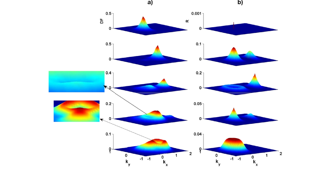
Results. We introduce the dimensionless time parameter given by
where
is the approximate time taken for the distribution to complete one “trip”.
Fig. 2a shows the time evolution of the distribution function distribution (DF) for (), in the absence of low energy scattering (). At the initial distribution is the tail of the Fermi distribution in the conduction band (Eq. 12), which is Maxwellian-like, and drifts along the direction (opposite to the -field) to reach the OP energy at (second panel). At that time, a “hump” appears around (not yet visible on the DF graph) as the front electrons reach region II, where they emit OP’s and scatter back inside region I, as seen in the second panel of fig. 2b. As time progresses , the “hump” develops into a dimple, while the remaining high energy electrons from the first trip continue their drift in region II, where they experience strong OP depopulation. As seen in the third panel of fig. 2b, the corresponding repopulation rate at low energy exhibits a crater-like shape, which is due to the randomizing nature of the deformation potential OP scattering. Indeed, as schematically shown in fig.1b, after OP emission by high energy electrons, all -values become equiprobable, which forms a drifting circle of high repopulation rate, with increasing k-radius as first trip electrons penetrate deeper in region II. This crater-like feature of the repopulation rate is the primary cause of the dimple in the low energy distribution function, which are areas in k-space where electrons have low probability to scatter. As time progresses, the DF “dimple” evolves into a crater-like shape, (fig.2.a, fourth and fifth panel), and the successive depopulation-repopulation OP processes overlapping at low energy with different amplitudes form also smooth terraces in the low energy tail of the distribution as it approaches steady state (fig.2.a , fourth panel). These morphological effects in electron distribution are unique to graphene as a result its linear band structure and the interplay of the quasi-ballistic acceleration and relaxation by high energy monochromatic OP’s.
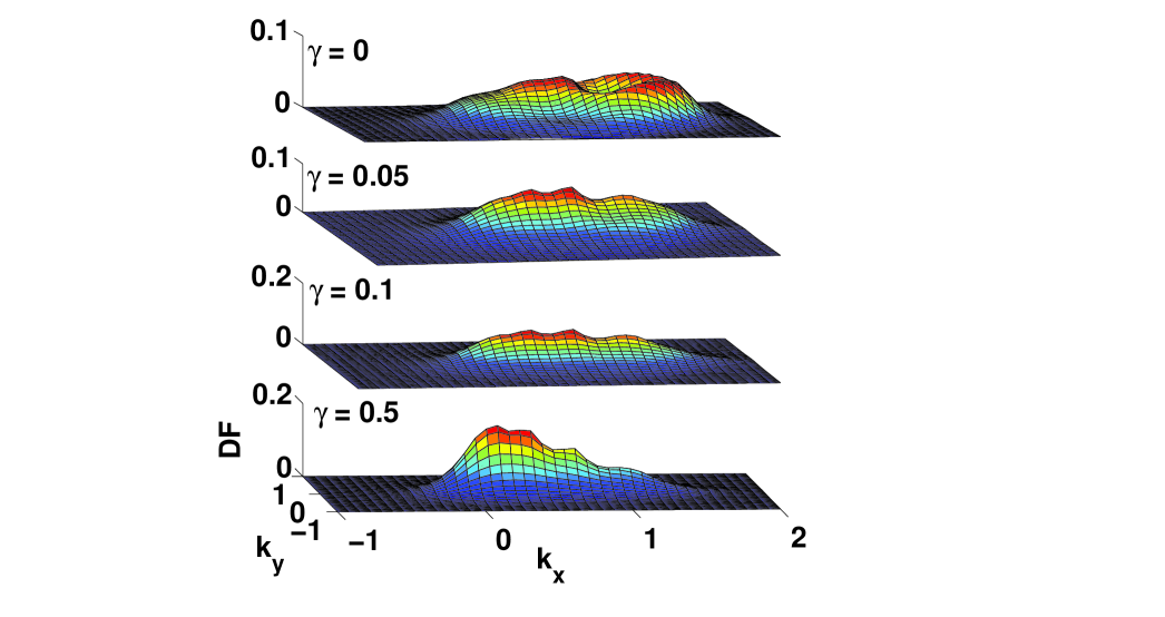
Fig. 3 shows snapshots of the distribution function at for varying low energy relaxation time, expressed in terms of . From the figure, one can see that the crater in the DF that occurs for progressively disappears as increases. Indeed low energy scattering in region I re-distributes charge carrier momenta around , especially in the crater center. For this reasons, the amplitude of the distribution in region I increases around . Also, the distribution amplitude decreases in region II () as carriers spend more time in region I (). Similarly the distribution recovers a streaming profile along the -direction as conventional semiconductors 8, 13. Nevertheless, even for strong damping (), the distribution is characterized by a jagged profile, which contains the front and back ridges of the crater remnant still caused by the cumulative effects of the OP scattering for backward and forward carrier relaxation.
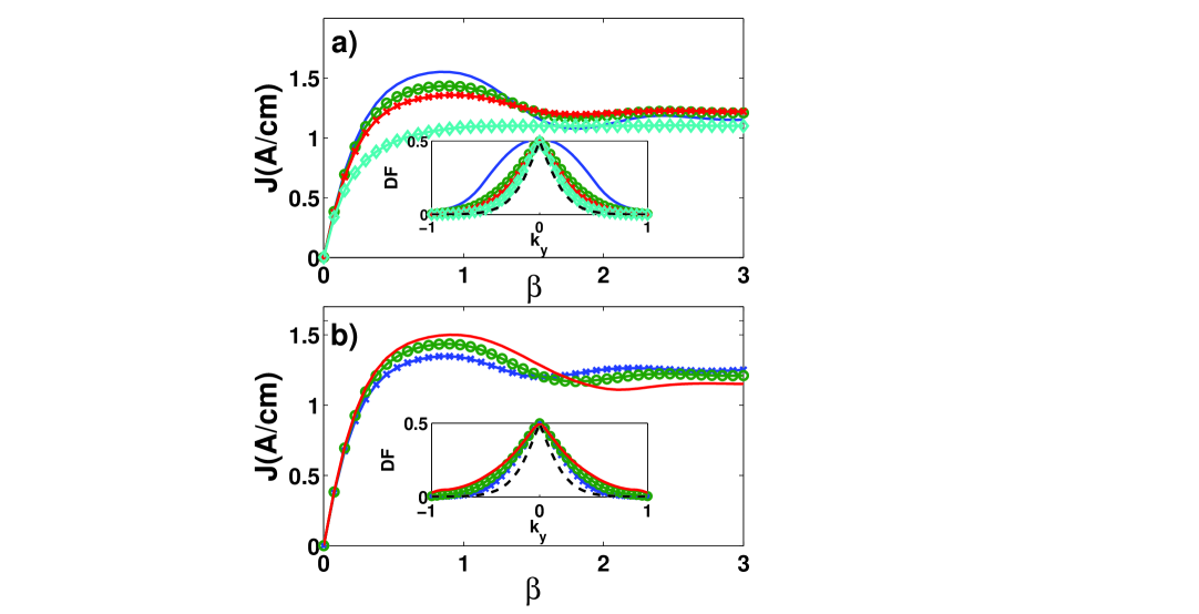
The current density on the plane is given by,
| (6) |
where is the angle between and the axis. Fig. 4a shows the current density as a function of time () for and different low energy scattering rates. For weak scattering, the current density overshoots its steady state value through damped oscillations, as a result of the back and forth motion of the distribution function (fig.1). The weaker the scattering, the higher the current overshoot. For strong low energy scattering, the current converges monotonically toward its steady state value without oscillations 8. Notice the stronger the scattering, the lower the steady state current value. The insert shows the corresponding DF cross-sections at and relative to the initial distribution at . As low energy scattering increases, the DF becomes narrower, taking a “streaming” profile in the electric field direction. This is due to the fact that as the low energy scattering increases, fewer electrons reach the high energy ( ) region II, reducing the number of electrons scattered back to the low energy region I, which narrows the distribution.
Fig. 4b shows the current density as a function of time for three different field values, with in each case. One observes that the oscillation period scales with the inverse of the electric field . Also quite expectedly, the overshoot value increases with electric fields, but the damping is also enhanced with electric fields, which is due to the fact that the electron distribution penetrates the high energy() region(II) farther than , stretching the carrier relaxation by OP emission, which in turn broadens the DF in region I along the field, thereby reaching steady state quicker. The insert shows the DF cross-sections at and for the different fields, relative to the initial distribution at . As the field is increased, the distribution function broadens, because more electrons reach the high-energy ( ) region II, and scatter back into region I broadening the distribution in the process.
The average energy density of carriers in the conduction band is given by,
| (7) |
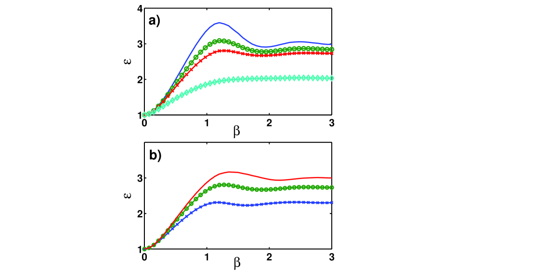
where is the overall normalized distribution function, and the summation is taken over all in regions I and II. At , the average energy per charge carrier is found to be . This value is roughly twice larger than expected for two-dimensional systems, and is the direct consequence of the linear energy dispersion in graphene, by contrast to the parabolic dispersion in normal 2D systems. Fig. 5a displays the ratio for and different low energy scattering rate (). As expected, the energy converges to higher values as low energy scattering is reduced. In addition, the convergence toward steady state occurs through damped oscillations, even for as a consequence of the back and forth motion of the DF between the OP energy and the carrier zero-point energy. Quite clearly the oscillation period is given by for all . It is also seen that the oscillations persist even with significant low energy scattering. Fig. 5b displays the normalized energy as a function of time for different fields and . As expected, carrier energies reach higher values as the field is increased, and the oscillation period decreases (larger -period).
Discussions. We have provided a transient analysis of the onset of current oscillations at the electric field turn-on caused by the back and forth motion of carrier distribution function between the zero-point energy and OPs in the presence of varying damping mechanisms. In this context we point out the anomalous shape of the carrier distribution as an interplay between ballistic acceleration and deformation potential OP emission in the transient regime. If OP-limited current oscillations have been predicted in GaAs, 8 and indirectly observed in slightly n-doped InSb 14, their manifestation in graphene is different in several respects: First, owing to the linear carrier energy-momentum dispersion, the oscillation periodicity is given by in graphene, while in GaAs parabolic conduction band it is expressed as , which nevertheless yields similar values, since the small effective mass, and the OP phonon frequency in GaAs compensate for the large 8, 10. Second, in III-V semiconductors, the OP polar nature focuses the low-energy repopulation along the axis, which provides a “streaming” profile to the carrier distribution instead of a crater-like shape in this case. Finally, in compound semiconductors, the oscillation onset is restricted by two conflicting conditions: On the one hand, the low value of the OP energy () is comparable to the thermal broadening of the carrier distribution at room temperature so that the back and forth motion of the distribution between the optic phonon and the zero point energy is immediately damped 8, 9, 10. On the other hand, at low temperature, ionized impurity scattering becomes dominant and produces strong damping which can only be reduced by lowering the dopant density, thereby lowering the carrier density, and weakening the oscillation amplitude. In this respect, the high conductance of graphene, and the high optic phonon energy provide the conditions for room temperature observation.
Low energy scattering should however still be minimized. Usually, for experimental studies and device applications, graphene-layers rest on a dielectric substrate, or are confined between two dielectric slabs 15, 16. In this case the presence of high K-dielectrics sandwiching the strictly 2-D graphene-layer may be used to screen charged impurity that may reduce low energy elastic scattering 17. However, dielectrics also contain interface and remote static charges that may offset dielectric screening 18. Moreover, the interaction between the 2D carriers in graphene and low energy Remote Interface Phonon (RIP) arising from the proximity of the substrate 19, 20 introduces new scattering sources 21, 22. Therefore in general, suspended graphene-layers avoiding the RIP influence may be preferable 23.
In this context to be observable at room temperature, the velocity oscillations should also take place within a parameter window. On the one hand the process requires where is the external bias, to reach the OP energy, and on the other hand, the field should be large enough for carriers to escape low energy scattering, but where is the OP scattering rate, so that charge carriers don’t penetrate the high-energy region , scatter immediately after they reach the OP energy, which maintains the coherence of the distribution function. These requirements impose a lower and upper bound on the electric field, i.e. (in graphene), and a lower bound on the sample length (m for ), but should be smaller than a few values of , so as to prevent oscillation damping.
One important issue for the validity of this analysis is the effect of leakage current due to electrons in the valence band crossing to the conduction of carriers through the Dirac point. Indeed it has been shown that there is still a minimum conductance () between the two bands despite the singular nature of the Dirac point 24. This value was later measured to be 1. However, this effect becomes important only when the graphene layer width , for which the band gap are vanishing. Moreover, thermal effects such as acoustic phonon absorption by carriers in the valence band, are forbidden by conservation of both, energy and momentum. As for OP absorption we have shown earlier their occupation number is also negligible over the time scale considered in this analysis.
Samwel K. Sekwao, thanks the Physics Department at the University of Illinois for continued support throughout this research project.
References
- Novoselov et al. 2005 Novoselov, K. S.; A. K. Geim, S. V. M.; Jiang, D.; Katsnelson, M. I.; Grigorieva, I. V.; Dubonos, S. V.; Fristov, A. A. Nature (London) 2005, 438, 197
- Katsnelson 2007 Katsnelson, M. I. Materials Today 2007, 10, 20
- Saito et al. 1998 Saito, R.; Dresselhaus, G.; Dresselhaus, M. S. Physical Properties of Carbon Nanotubes; Imperial College Press, 1998
- Tiwari 1992 Tiwari, S. Compound Semiconductor Device Physics; Academic Press: San Diego, CA, 1992
- Piscanec et al. 2007 Piscanec, S.; Lazzeri, M.; Mauri, F.; Ferrari, A. Eur. Phys. J. Special Topics 2007, 148, 159
- Kartheuser 1971 Kartheuser, E. Polarons in Ionic Crystals and Polar Semiconductors; American Elsevier: NATO Advanced Study Institute, Antwerp, 1971; pp 717 – 733
- Shockley 1951 Shockley, W. Bell System Technical Journal 1951, 30, 990
- Matulionis et al. 1975 Matulionis, A.; Pozela, J.; Reklaitis, A. Physica Status Solidi (a) 1975, 31, 83
- Brauer 1977 Brauer, M. Physica Status Solidi (b) 1977, 81, 147
- Leburton and Evrard 1978 Leburton, J.; Evrard, R. Journal of Low Temperature Physics 1978, 32, 323
- Neto et al. 2009 Neto, A. H. C.; Guinea, F.; Peres, N. M. R.; Novoselov, K. S.; Geim, A. K. Review of Modern Physics 2009, 81, 109
- Datta 1989 Datta, S. Quantum Phenomena; Addison-Wesley, 1989
- Devreese and Evrard 1976 Devreese, J. T.; Evrard, R. Physica Status Solidi (b) 1976, 78, 85
- Lochner 1972 Lochner, H. Journal of Applied Physics 1972, 43, 3585
- Meric et al. 2008 Meric, I.; Han, M. Y.; Young, A. F.; Ozyilmaz, B.; Kim, P.; Shepard, K. L. Nature Nanotechnology 2008, 3, 654
- Oostinga et al. 2007 Oostinga, J. B.; Heersche, H. B.; Liu, X.; Morpurgo, A. F.; Vandersypen, L. M. K. Nature Materials 2007, 7, 151
- Jena and Konar 2007 Jena, D.; Konar, A. Physical Review Letter 2007, 98, 136805
- Ponomarenko et al. 2009 Ponomarenko, L. A.; Yang, R.; Mohiuddin, T. M.; Katsnelson, M. I.; Novoselov, K. S.; Morozov, S. V.; Zhukov, A. A.; Schedin, F.; Hill, E. W.; Geim, A. K. Physical Review Letter 2009, 102, 206603
- Hess and Vogl 1979 Hess, K.; Vogl, P. Solid State Communications 1979, 30, 807
- Leburton and Dorda 1981 Leburton, J.; Dorda, G. Solid State Communications 1981, 40, 1025
- Fratini and Guinea 2008 Fratini, S.; Guinea, F. Physical Review B 2008, 77, 195415
- Fischetti et al. 2001 Fischetti, M. V.; Neumayer, D. A.; Cartier, E. A. Journal of Applied Physics 2001, 90, 4587
- Bolotin et al. 2008 Bolotin, K.; Sikes, K.; Jiang, Z.; Klima, M.; Fudenberg, G.; Hone, J.; Kim, P.; Stormer, H. Solid State Communications 2008, 146, 351
- Fradkin 1986 Fradkin, E. Physical Review B 1986, 33, 3263