Stacking Order dependent Electric Field tuning of the Band Gap in Graphene Multilayers
Abstract
The effect of different stacking order of graphene multilayers on the electric field induced band gap is investigated. We considered a positively charged top and a negatively charged back gate in order to independently tune the band gap and the Fermi energy of three and four layer graphene systems. A tight-binding approach within a self-consistent Hartree approximation is used to calculate the induced charges on the different graphene layers. We found that the gap for trilayer graphene with the ABC stacking is much larger than the corresponding gap for the ABA trilayer. Also we predict that for four layers of graphene the energy gap strongly depends on the choice of stacking, and we found that the gap for the different types of stacking is much larger as compared to the case of Bernal stacking. Trigonal warping changes the size of the induced electronic gap by approximately 30% for intermediate and large values of the induced electron density.
pacs:
73.22.PrI Introduction
Graphene is a single layer of carbon atoms with hexagonal symmetry novoselov . Multilayers of graphene can be stacked differently depending on the horizontal shift between consecutive graphene planes, leading to very different electronic properties latil , e.g. to various band structures.
A perpendicular electric field applied to bilayer graphene, with the AB stacking, can open an electronic gap between the valence and conduction bands mccann . This was shown indirectly by transport measurements castro ; lieven . Later on, spectroscopic measurements confirmed the opening of a gap in the energy spectrum ohta_Science ; Li ; zhang ; kuzmenko ; zhang_Nature . The extension of these bilayer results to three and four layers of graphene was presented in Ref. Avetis, in the case the perpendicular electric field was realized by a single gate. It was found that such an electric field causes an energy gap which was found to be a nonmonotonic function of the gate voltage, and a reentrant opening and closing of the gap was predicted as a function of the electric field strength. In Ref. koshino the electronic band structure of the ABA-stacked trilayer graphene in the presence of back and top gates was invistigated.
Recently, we generalized our previous results Avetis to the case when two, i.e. top and back, gates were applied to three as well as to four layers of graphene systems Avetis2 . We found that due to the trigonal warping the obtained results do not exhibit electron-hole symmetry. A non-monotonic dependence of the true energy gap in trilayer graphene on the charge density on the gates was found. We also predicted an indirect gap with a non-monotonic dependence on the gate voltage. Four layers of graphene exhibit a larger energy gap as compared to the three layer system, which is a consequence of the fact that Dirac fermions are present in the AB stacked graphene multilayers in case of an odd number of layers, while for an even number of stacked graphene layers only charge carriers with a parabolic dispersion are present at low energies partoens7 .
Using Raman spectroscopy measurements the graphitic flake thickness, i.e. the number of graphene layers, can be obtained, as was demonstrated in Refs. gutt, and graf, . In Ref. gutt, a tunable three-layer graphene single-electron transistor was experimentally realized showing a transport gap near the charge neutrality point. To our knowledge, up to now, no four layer system was studied experimentally. Electrical tunable energy gap systems are of interest from a fundamental point of view, but also for possible applications in electronics (e.g. for transistors) and photonics (i.e. wavelength tuning of a laser).
The electronic low-energy band structure of the ABC stacked multilayer graphene was studied within an effective mass approximation in Ref. koshino1, , with special attention to the Lifshitz transition, in which the Fermi circle breaks up into several pockets.
In this paper we study the effect of different ways of stacking of multilayers of graphene on the electric field induced band gap by top and back gates. We limit ourselves to those stackings that have been found in graphite. The Bernal stacking (ABA), which has hexagonal symmetry, is common and stable, but some parts of graphite can also have rhombohedral one (the ABC stacking) Lipson . The band structure of three and four layer graphene systems in the presence of a perpendicular electric field is obtained using a tight-binding approach, where we used a self-consistent Hartree approximation to calculate the induced charges on the different graphene layers. We found that the gap for trilayer graphene with the ABC stacking is much larger than the one for the ABA stacking, which was studied in Ref. Avetis2, .
Similarly for four layers of graphene the energy gap also strongly depends on the choice of stacking, and is smallest in case of Bernal stacking. When taking into account the circular asymmetry of the spectrum, which is a consequence of the trigonal warping, we found considerable changes in the size of the induced electronic gap for the considered systems at intermediate and high densities of total electrons induced on the layers.
This paper is organized as follows. A short overview of our tight-binding approach with a description of the self-consistent calculation are given in Sec. II for the ABC stacked three layer graphene in the presence of top and back gates. The corresponding numerical results are also discussed here. In Sec. III we investigate four layer graphene with different stacking order in the presence of top and bottom gates. Sec. IV summarizes our conclusions.
II Three layer graphene with the stacking in an external electric field
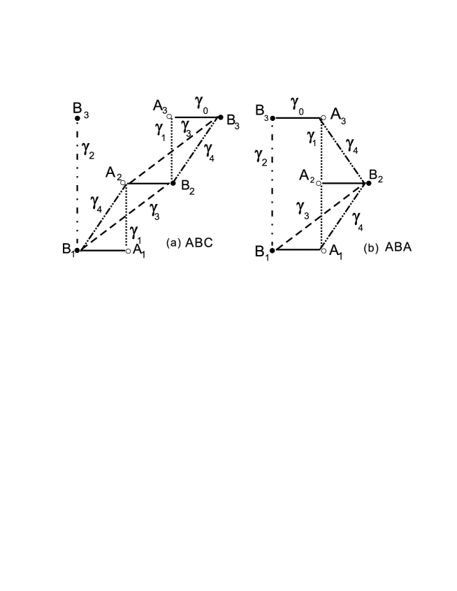
We consider a system consisting of three layers of graphene with the ABC stacking, which is modeled as three coupled hexagonal lattices with inequivalent sites and ( is the layer number) with and , as well as and atoms on top of each other, as shown in Fig. 1. We use the Slonczewski-Weiss-McClure (SWMcC) parameters, i.e. of tight-binding couplings for bulk graphite. Within each layer the interaction between nearest neighbor and atoms is described by the parameter . The strong coupling between nearest layers, i.e. between and atoms that lie directly above or below each other is given by , and the weaker nearest layer coupling by (), i.e. between sites and (, , and ). The interaction between the next nearest layers () is determined by , as is shown in Fig. 1(a) and for comparison in Fig. 1(b) we show the unit cell for the ABA trilayer. Using these parameters we compose the tight-binding Hamiltonian for three layer graphene with the ABC stacking, which has the form guinea
| (1) |
where the rows and columns are ordered according to atom from layer 1, atom from layer 1, atom from layer 2, atom from layer 2, etc, with the following two by two matrixes:
| (2a) |
| (2b) |
| (2c) |
where
| (3) |
with the in-plane lattice vector length. The Hamiltonian for the ABA stacking was discussed in Ref. Avetis2, .
To control the density of electrons on the different graphene layers and independently the Fermi energy of the system, a top gate with a density of negative charges (the electron excess density is positive) on it, and a back gate with a density of positive charges are applied to the trilayer (a schematic picture was presented in Fig. 1 of Ref. Avetis2, ). As a result a total excess density is induced (), with the excess density on the closest layer to the top gate, on the closest layer to the back gate, and is the excess density on the middle layer. In our model the top or back gate produces a uniform electric field , and due to the induced charges on the graphene layers, in its turn, create fields with the permittivity of vacuum and the dielectric constant. There is a simple relation between the charge density on the gates and the voltage between the gate and the closest graphene layer: , where is the distance from the gate to the closest graphene layer (usually is equal to the oxide thickness, which is typically about 300nm). For our numerical calculations we use the value , which corresponds to graphene layers on . The difference between the charge densities induced on the individual layers of graphene creates asymmetries between the first and the second layers, as well as between the second and the third layers, which are determined by the corresponding change in the potential energies and
| (4a) |
| (4b) |
where , with the inter-layer distance. The Hamiltonian Eq. (1) in the presence of the top and back gates is modified and we have to add , and to the first and third layer on-site elements in Eq. (1). The tight binding Hamiltonian operates in the space of coefficients of the tight binding functions , where and are the -th layer coefficients for and type of atoms, respectively. The total eigenfunction of the system is then given by
| (5) |
with the number of layers. By diagonalizing the Hamiltonian one can obtain the six coefficients (in Eq. (5)) for fixed values of the layer asymmetries, from which we obtain the excess electronic densities on the individual layers:
| (6) |
The coefficients and depend on the energetic band index. Here we are interested in the case when the Fermi energy is located in the band gap, and in order to find the redistribution of the electron density over the different layers in the valence bands one should integrate Eq. (6) over the Brillouin zone. The Fermi energy can be tuned into the opened gap, when the magnitudes of the top and back gates are equal to each other but with opposite charges on them. The other case when the Fermi energy is located in the conduction or valence band was discussed in Ref. Avetis2, for the ABA stacked trilayer where we found that the obtained results do not exhibit electron-hole symmetry in the presence of trigonal warping. Using Eqs. (1-4b) and (6) we evaluate the energy gap at the -point and the true gap, , self-consistently for a fixed total density (see Refs. mccann, and Avetis2, ).
In the following we will consider two cases. Firstly, we neglect all interactions except between the nearest neighbour atoms in the same layer and between the atoms of adjacent layers which are on top of each other, i.e. we put . This leads to a circular symmetric spectrum. In our calculations we used the parameter which leads to an in-plane velocity m/s, and for the interlayer coupling strength, we take eV (see Ref. partoens, ), and for the interlayer distance . Secondly, the full interaction case is studied where the interaction between the different atoms is expressed by the SWMcC parameters (), i.e. the effect of warping is included.
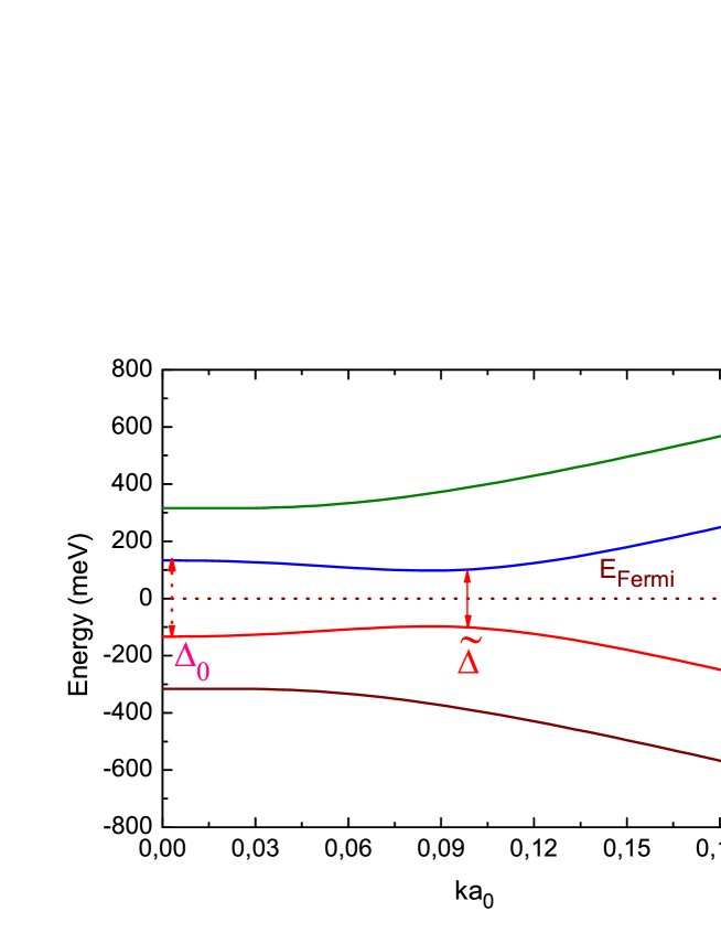
Fig. 2 shows the band structure for trilayer graphene with the ABC stacking when charges on the top and back gates are opposite but equal in magnitude with when only are taken into account (with ), and the Fermi energy is located in the forbidden gap. Notice that there is conduction band - valence band symmetry around the Fermi energy, and the true gap occurs away from the -point where the gap is . For the ABA stacking for the case when only the true gap is zero for all densities.
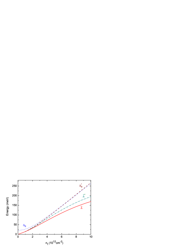
When all the interactions between the different atoms are taken into account the surface of constant energy is no longer circular. In Fig. 3 we show the gap at the -point (dotted blue curve), and the true direct gap (solid red curve) for trilayer graphene with the full interaction, as a function of the top gate density providing the back gate density . For comparison in the same figure we show also the corresponding results, (dashed red curve) and (dot-dashed blue curve) when only . Notice, that for high densities () the inclusion of the full interaction leads to a lowering of the true gap by 30%. It is interesting to note that similar values for the energy gaps and the relative difference between them was found for the case of bilayer AB graphene Avetis2 : the true gap for the AB bilayer at is when and for the case of , when the full interaction is included. These results compare with () and () for our ABC trilayer.
This similarity becomes more remarkable, if we compare the layer densities induced by external gates for the ABA and ABC trilayers with the AB bilayer. For the ABA trilayer, when only a back gate was applied to the first layer Avetis , we found that , and at (in units ). The small amount of excess charges on the last layers was explained by the fact that the graphene layers screen the electric field and the layer asymmetries between the last layers, counted from the gate, are very small. The true gap for this system () is smaller in comparison with the bilayer case, where for the latter and (). Now, when only a back gate is applied to the ABC trilayer we find that the densities on the second and the third layers (counted from the back gate) are very close to each other: at and , which makes the ABC system distribution and the gap (with ) similar to the AB bilayer ones. In Fig. 1(a) one can see that in the case of the ABC stacking there are never 3 atoms stacked on top of each other, as in the case for the ABA. As a result the electric field (of the gate located near the first graphene layer for the ABC stacking) penetrates easier to the last layers inducing excess charges, while for the ABA stacking the electric field is much more strongly screened.
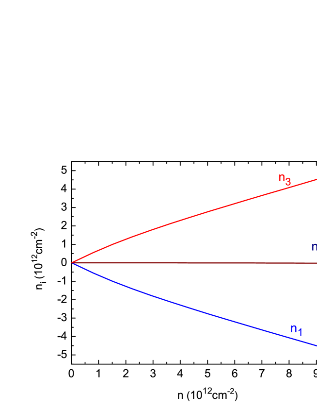
When both gates are applied to the ABC trilayer graphene (when the full interaction is included) the excess charge densities at , shown in Fig. 4, on the outer layers are and in the middle layer is zero. Notice, that the excess charge densities on the bottom and the top layers are symmetric as in the case of the AB bilayer, as well as the gaps have also similar values. While for the ABA trilayer it was and Avetis2 , and when ; the inclusion of the full interaction in the ABA case makes the excess electron density in the middle layer different from zero, and it opens a small gap about . So, we see that the ABC system has a large gap, comparable with the AB bilayer one and behaves as a bilayer with shifted sheets, while the ABA opens up much smaller gap and is similar to the case of an AA stacked bilayer.
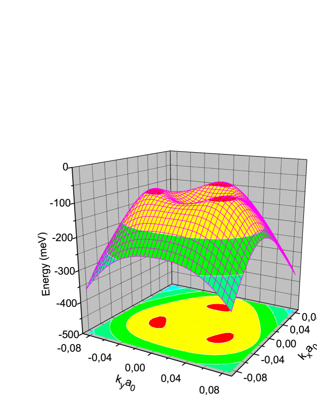
In the case of the previous studied ABA trilayer Avetis the inclusion of trigonal warping leads to a non-monotonic behaviour of the gaps as a function of gate voltage, as well as a much stronger lowering of the true gap. Here, we found that the energy gaps for the ABC stacked trilayer is much larger as compared to the case of the ABA trilayer. Fig. 5 shows a -plot and the corresponding contourplot of the highest valence band for three layer ABC stacked graphene near the -point (-point is chosen as the origin, ) for . The lowest conduction band is again symmetric with the highest valence band just as in the case when only . Here, for the ABC stacking we find three maxima, but did not find additional maxima as in the case of the ABA stacking Avetis2 and as a result we do not observe an indirect gap.
III Four layer graphene system in an external electric field
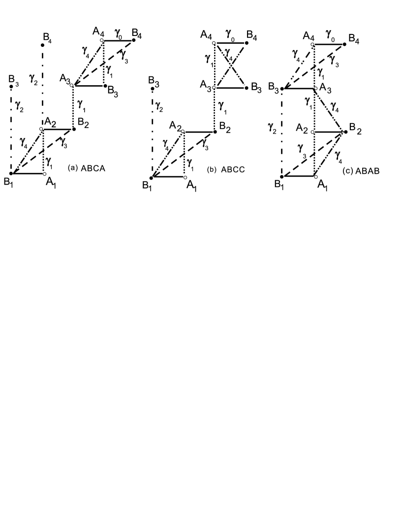
Now, we consider the four layer graphene system, which can be arranged in many different ways as schematically shown in Figs. 6(a-c). The tight-binding parameters and the interaction between the individual carbon atoms for all these cases are indicated in these figures. Four layer graphene is described by the Hamiltonian
| (7) |
where and with are the matrix elements of the ABC trilayer given by Eqs. (2a-2b) and for the ABCA stacking we have
| (8a) |
| (8b) |
while for the ABCC stacking these matrixes have the following form:
| (9a) |
| (9b) |
We consider a four layer graphene system with top and back gates, which induce a total excess density , where is the excess density on the th layer as counted from the top gate. The corresponding change in the potential energy between consecutive layers is
| (10a) |
| (10b) |
| (10c) |
By adding , and to the on-site elements of the , and layer of the ABCA or the ABCC four layer Hamiltonian, respectively, we obtain the Hamiltonian in the presence of top and bottom gates. The eight coefficients and , for fixed values of the layer asymmetries defined by Eqs. (10a-10c), can be obtained by diagonalizing the corresponding Hamiltonian. The electronic densities on the individual layers are given by Eq. (6). The gaps , are evaluated self-consistently analogously as was done for the three layer system.
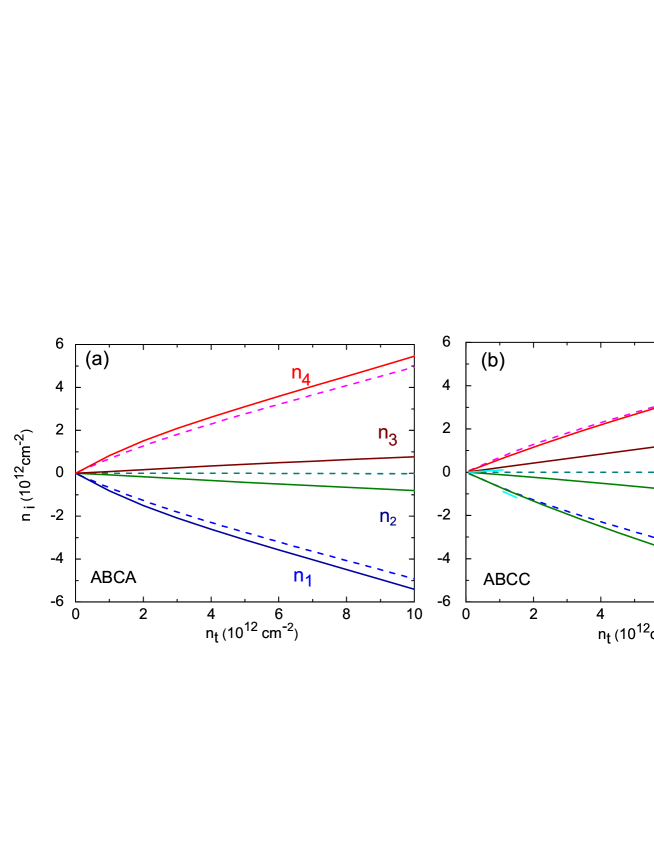
The variation of the gap at the -point (dot-dashed red curve), the true direct gap (solid red curve) and the true indirect gap (dotted blue curve) with the top gate density () for four layer graphene with the full interaction is shown in Fig. 7(a) for the ABCA stacked four layer graphene and in Fig. 7(b) for the ABCC stacking. One can see that for the ABCA stacking with full interaction the true direct gap is very close to the corresponding gap in the case of a trilayer with the ABC stacking, e.g., for the true gap is about for four layer graphene with the ABCA stacking and for the ABC trilayer it is . In Figs. 8(a) and 8(b) we present the layer densities for the ABCA and ABCC four layer graphene systems, respectively, and we include the curves for the densities in the ABC stacked trilayer for comparison in both figures (dashed curves). It is remarkable that the excess densities for the ABCA system on the outer as well as on the inner layers are symmetric. Notice, that the densities, shown in Fig. 8(a), on the outer layers for the ABCA are very close to the ABC trilayer graphene ones for all the values of : at for the ABCA , while for the ABC trilayer graphene (in the units ). We see that also the ABCA four layer graphene behaves as the AB bilayer. The localization of the atoms (see Fig. 6) can explain why the excess electron densities on the outer sheets for the ABCA system are larger than the densities for the ABC trilayer, and even in comparison with the AB bilayer densities (which has at ). For the ABCA system there are never 4 atoms on top of each other, as is the case for the ABAB stacking. As a consequence, the electric field of the top gate, e.g. at (see Fig. 6(a)) is screened only by the atom. Similarly, the field of the back gate at is screened only by atom. As a result, both these atoms feel the field of the top as well as the back gate, which leads to a decrease of excess charges on the inner layers (i.e. to a neutralization of these charges by the opposite gates). However, an outer layer (of the ABCA system) which is mainly charged by its closest gate does not feel the further located gate, since the latter is screened by the inner layers. In the AB bilayer the two sheets feel both gates, and consequently the excess charges (by absolute value) are less than in the outer layers of the ABCA. Due to this, also the gap for the AB bilayer is less (see the gap value in previous Section) than the ABCA one (for the same strength of the top and back gates). We see also, that the gap is large when the amount of excess charges in the inner layers is small (as it is for the ABCA system). We found also that for the true gap is for the ABCA; the relative difference with the case of is only about 5%.
In contrast, for the ABCC four layer graphene the excess density on the third layer is larger, and on the fourth layer is smaller than the corresponding densities found in the case of the ABCA system. So, the increase in the excess densities as well as the density asymmetry in the inner sheets leads to a decrease of the gap. Also, the fact that the third and fourth sheets are not shifted, i.e. they have the AA stacking order, explain that in the ABCC four layer graphene the electric field opens up a smaller gap. In both cases we found a much larger gap (about for the ABCA stacking and for the ABCC stacking at ) than in the case of the ABAB stacked four layer graphene Avetis2 (with for the same density). So, we see that from all the systems, considered in this paper and in Ref. Avetis2, , the Bernal stacking leads to the smallest gap.
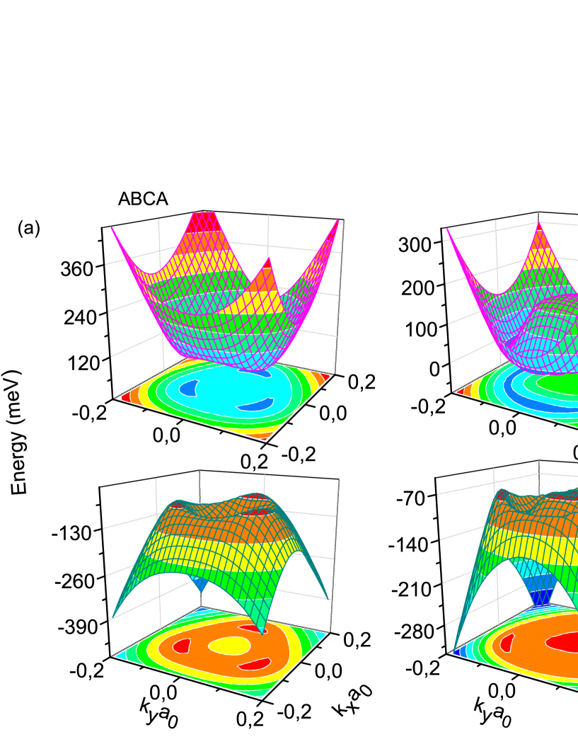
Figs. 9(a) and (b) show -plots and corresponding contourplots of the highest valence and the lowest conduction bands near the -point (-point is chosen as the origin, ) in the case of , for the ABCA and the ABCC stacking, respectively. The conduction band for the ABCC stacking has a ”Mexican hat” shape maxima and minima on a ring, as shown in the contourplot, e.g. there is a minimum at and . In its turn the valence band has a local minimum between the two maxima at the plane . The asymmetry between the contourplots for the conduction and the valence bands for the ABCC (see Fig. 9(b)) leads to an indirect true gap. At low densities there is a true direct gap for the ABCC, but due to the overlap between the bands at different points in -space the indirect gap is negative as is shown in Fig. 7(b), i.e. we have a semi-metal for low gate densities. For the ABCA we find only three minima in the conduction band and a symmetric valence band (see Fig. 9(a)), analogously with the ABC trilayer case. For the ABCA system the indirect gap is smaller than the direct one at low densities, and they coincide at high densities.
When finishing this paper we came aware of a recent preprint koshino2 on the effect of an electric field on multilayers of graphene with different stacking. They used the simplest approximation where only . They argued that the inclusion of the other tight-binding parameters do not affect strongly the band structure and the true gap. However, our calculations show that the true gap can be changed by 30%.
IV Conclusions
The effect of different stacking order on the electric field induced energy gap of three and four layers of graphene was investigated. For three- as well as for four-layer graphene the energy gap strongly depends on the choice of stacking, and we found that the gap is much larger than for the previously studied Bernal stacking. We found that the true gap for the ABC trilayer and the ABCA four layer graphene is comparable with the corresponding gap for bilayer graphene with Bernal stacking. The account of the circular asymmetry of the spectrum, which is a consequence of the trigonal warping, considerably changes the size of the induced electronic gap for the studied systems.
Acknowledgements.
This work was supported by the Flemish Science Foundation (FWO-Vl), the “Belgian Science Policy” IAP-program, and the Brazilian Science Foundation CNPq. One of us (AAA) was supported by the Belgian Federal Science Policy Office.References
- (1) K. S. Novoselov, A. K. Geim, S. V. Morozov, D. Jiang, M. I. Katsnelson, I. V. Grigorieva, S. V. Dubonos, and A. A. Firsov, Nature (London) 438, 197 (2005).
- (2) S. Latil and L. Henrard, Phys. Rev. Lett. 97, 036803 (2006).
- (3) E. McCann, Phys. Rev. B 74, 161403(R) (2006).
- (4) Eduardo V. Castro, K. S. Novoselov, S.V. Morozov, N. M. R. Peres, J. M. B. Lopes dos Santos, Johan Nilsson, F. Guinea, A. K. Geim, and A. H. Castro Neto, Phys. Rev. Lett. 99, 216802 (2007).
- (5) J. B. Oostinga, H. B. Heersche, X. Liu, A. F. Morpurgo, and L. M. K. Vandersypen, Nature Mater. 7, 151 (2008).
- (6) T. Ohta, A. Bostwick, T. Seyller, K. Horn, and E. Rotenberg, Science 313, 951 (2006).
- (7) Z. Q. Li, E. A. Henriksen, Z. Jiang, Z. Hao, M. C. Martin, P. Kim, H. L. Stormer, and D. N. Basov, Phys. Rev. Lett. 102, 037403 (2009).
- (8) L. M. Zhang, Z. Q. Li, D. N. Basov, M. M. Fogler, Z. Hao and M. C. Martin, Phys. Rev. B 78, 235408 (2008).
- (9) A. B. Kuzmenko, E. van Heumen, D. van der Marel, P. Lerch, P. Blake, K. S. Novoselov, and A. K. Geim, Phys. Rev. B 79, 115441 (2009).
- (10) Y. Zhang, T.-T. Tang, C. Girit, Z. Hao, M. C. Martin, A. Zettl, M. F. Crommie, Y. R. Shen, and F. Wang, Nature (London) 459, 820 (2009).
- (11) A. A. Avetisyan, B. Partoens, and F. M. Peeters, Phys. Rev. B 79, 035421 (2009).
- (12) M. Koshino and E. McCann, Phys. Rev. B 79, 125443 (2009).
- (13) A. A. Avetisyan, B. Partoens, and F. M. Peeters, Phys. Rev. B. 80, 195401 (2009).
- (14) B. Partoens and F. M. Peeters, Phys. Rev. B 75, 193402 (2007).
- (15) J. Guttinger, C. Stampfer, F. Molitor, D. Graf, T. Ihn, and K. Ensslin, New J. Phys. 10, 125029 (2008).
- (16) D. Graf, F. Molitor, K. Ensslin, C. Stampfer, A. Jungen, C. Hierold, and L. Wirtz, Nano Lett. 7 238, (2007)
- (17) M. Koshino and E. McCann, Phys. Rev. B 80, 165409 (2009).
- (18) H. Lipson and A. R. Stokes, Proc. Roy. Soc. A181, 101 (1942).
- (19) F. Guinea, A. H. Castro Neto, and N. M. R. Peres, Phys. Rev. B 73, 245426 (2006).
- (20) B. Partoens and F. M. Peeters, Phys. Rev. B 74, 075404 (2006).
- (21) M. Koshino, cond-mat/0911.3484v1 (2009)
.
