Mechanisms of doping graphene
Abstract
We distinguish three mechanisms of doping graphene. Density functional theory is used to show that electronegative molecule like F4-TCNQ and electropositive metals like K dope graphene p- and n-type respectively. These dopants are expected to lead to a decrease in carrier mobility arising from Coulomb scattering but without any hysteresis effects. Secondly, a novel doping mechanism is exhibited by Au which dopes bilayer graphene but not single layer. Thirdly, electrochemical doping is effected by redox reactions and can result in p-doping by humid atmospheres and n-doping by NH3 and toluene.
1 Introduction
The type and concentration of carriers in graphene can be controlled by adsorbates or substrates which transfer charge to graphene. -type electronic doping results from a disparity between the work function of graphene and the electron affinity of the adsorbate. In the simplest case this is caused by a difference between the highest occupied molecular level (HOMO) and the lowest unoccupied molecular level (LUMO) of the adsorbate and graphene. This alignment as we shall see can depend on the substrate as we shall show that Au dopes bilayer graphene but is ineffective for single layer graphene. Electrochemical doping results from redox reactions near the graphene surface. The timescales for the two types of doping is different since electronic doping occurs spontaneously while electrochemical doping requires longer times to overcome reaction and diffusion barriers. Hysteresis effects for graphene based field effect devices can also be expected in electrochemical doping since the concentration of the reactants can change at a rate slower than the change in gate voltages.
Electropositive elements like metals are good candidates for electronic n-type doping of graphene. Molecular beam deposition of transition metal clusters, Ti, Fe and Pt, has shown that these metals effect n-doping of graphene whereas bulk deposition of Pt dopes graphene p-type[1]. Electronic doping on graphene was also demonstrated with K atoms deposited at low temperatures (20K) on graphene in ultrahigh vacuum (UHV)[2]. Synchrotron-based high resolution photoemission spectroscopy (PES) showed that graphene can be made p-type by the deposition of tetrafluoro-tetracyanoquinodimethane (F4-TCNQ). Because of the molecular separation of the adsobate and graphene, all these dopants are expected to lead to a decrease in carrier mobility arising from Coulomb scattering without any hysteresis effects.
Exposure of graphene to a humid atmosphere or gaseous nitrogen dioxide leads to p-type behaviour, while ammonia leads to n-type behaviour [3]. A great surprise is that it was found, in particular experimental conditions, gaseous toluene leads to n-doping of graphene[4], in contradiction with theoretical calculations which predict no transfer of charge between graphene and the toluene molecule [12]. In this paper density functional calculations are used to investigate the transfer of charge between graphene and adsorbates. A electrochemical model for doping of graphene is also presented.
2 Method
The electronic ground state of graphene with different adsorbates was calculated using spin-optimised density functional theory as implemented in the AIMPRO code[5, 6]. The exchange correlation potential was described using the local density approximation (LDA). The core electron were treated using the Hartwigsen Goedecker Hutter (HGH) pseudopotencials[7]. The orbitals of the valence electrons consist of independent like Gaussian functions centred on atoms[8]. The electronic levels were filled using Fermi-Dirac statistics with =0.01 eV and a metallic filling. The Brillouin zone was sampled with a grid of 881 k-points within the Monkhorst-Pack scheme[9]. Charge densities were Fourier-transformed using plane waves with an energy cut-off of 200 Ha. The spin-populations of the cell were optimised by starting from random spin distributions. We used two different graphene unit cells, 441 and 661, enclosing 32 and 72 carbon atoms, respectively. During the relaxation all the atoms were allowed to move to their equilibrium positions. The influence of the cell size was also studied with larger supercells and the band structure obtained and the consequent charge transfer were very similar.
3 Electronic doping
The geometry of the relaxed F4-TCNQ molecule was found to be in good agreement with experimental results for its precursor TCNQ [10]. The electron affinity, the difference between the LUMO and the vacuum level, was found to be 5.25 eV in agreement with an experimental measurement of 5.2 eV[11]. This deep LUMO level when compared with the work function of graphene suggest that F4-TCNQ is a good candidate to act as an electronic acceptor on graphene.
The F4-TCNQ molecule was placed on top of a 72 carbon atoms graphene supercell, 661, and during the relaxation all the atoms were allowed to move. In the minimum energy configuration the molecule remain parallel to the graphene layer with a interplanar separation of 3.1 Å. The binding energy was found to be 1.26 eV which is probably overestimated as a result of the LDA approximation.
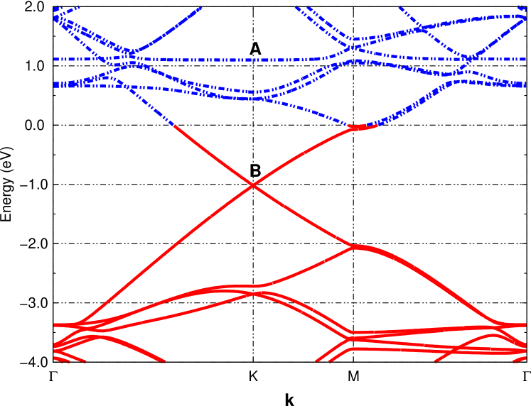
Figure 1 a) and b) shows respectively the electronic band structures of pristine graphene and graphene with an adsorbed molecule. Because of band folding, the Dirac point, where the and bonding and anti-bonding levels of graphene meet, occurs at instead of the K point in the 661 graphene supercell used here.
a)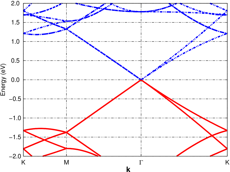 b)
b)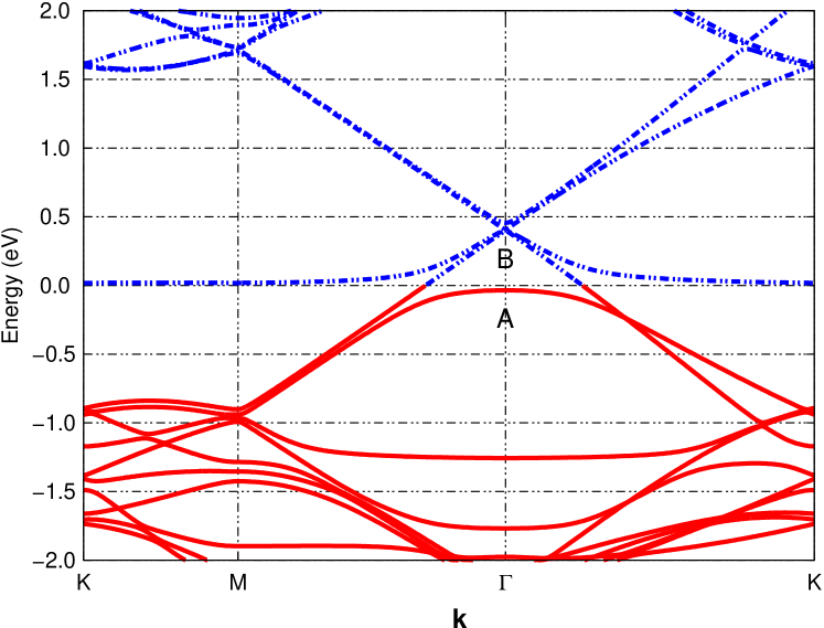
Comparison of the two electronic band structures shows that when the molecule is placed on top of graphene, the Fermi level is shifted to lie below the Dirac point, and a new filled flat band appears which is related to the adsorbate. This suggests transfer of negative charge from graphene to F4-TCNQ This is supported by an analysis of the wavefunction shown in Figure 2 a) of the level marked A in Figure 1 b). This shows that the new filled band is strongly localised on the F4-TCNQ molecule. In addition, the empty level marked B, which was occupied in graphene, is delocalised over the graphene layer. This confirms that charge transfer between graphene and F4-TCNQ occurs. The position of the Fermi-level indicates about 0.3 electrons are transferred from graphene to a molecule of F4-TCNQ.
a)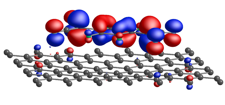 b)
b)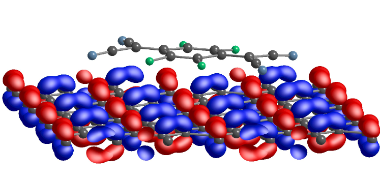
To study the doping properties of metals, a single atom of Au and K respectiverly were placed on graphene in the three obvious adsorption sites: above the centre of the graphene hexagonal ring, above a C-C bond and above the carbon atom. In the case of Au the minimum energy configuration was found to be 2.27 Å on top of a carbon atom whereas K sits 2.42 Å directly above the middle of a hexagon optimising the number of K-C bonds. Thus the K atom is strongly bound to graphene with a binding energy estimated to be 1.51 eV in contrast with the 0.65 eV estimated for a Au atom. This is in part due to their different doping properties. Spin-optimization led to a spin-less ground state for K and a spin-1/2 state for Au.
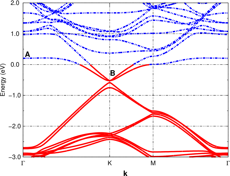
Figure 3 shows the electronic band structure of K on graphene. The Fermi level lies above the Dirac point which indicates doping of graphene with electrons. The wavefunction, shown in Figure 4 a), of the empty flat level marked A in Figure 3 is strongly localised on the K atom and is derived from the 4-level of K. The wavefunction (Figure 4 b)) of the filled level above the Dirac point, marked B is delocalised over the graphene layer. This confirms that K dopes graphene -type and we estimate about one electron per K atom is transferred.
a) 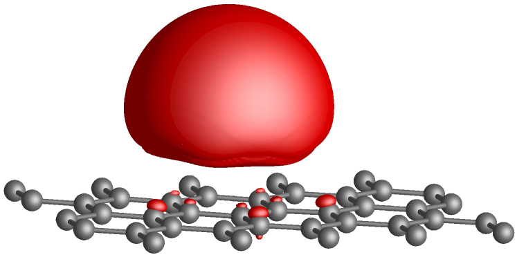
b) 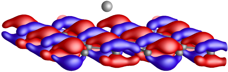
We now turn to doping with Au. Figure 5 a) and b) show the majority and minority spin electronic band structures for Au on graphene. Although there are changes to the dispersion of the bands in the vicinity of the Dirac point there is no significant change in the position of the Fermi level with respect to the Dirac point compared with pristine graphene. This implies that there is no significant charge transfer between Au and graphene.
a) 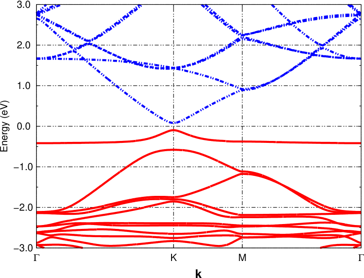 b)
b) 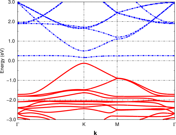
To study the effect of additional graphene layers, a single Au atom was placed between the AB stacked graphene bilayer. The relaxed ground state was spin-less and the Au atom occupied a site nearly midway between the two graphene layers and 2.14 Å directly above a carbon atom in the lower layer and directly below the middle of the hexagon of the top layer. The separation between the graphene layers increased to approximately 4.5 Å. The graphene sheets do not appear to appreciably distort. Figure 6 a) and b) show the electronic band strucuture of a pristine graphene bilayer and a graphene bilayer intercalated with Au atoms.
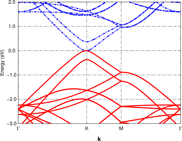
As for single layer graphene, the highest occupied and lowest empty bands touch at the Dirac point but the linear dispersion is lost. However, when the Au atom is placed between the graphene layers, the Fermi level is shifted above the Dirac point. An analyis of the wavefunction shows the flat level far from the K point, marked as A, results from the Au level. When the level crosses the bands of graphene, they hybridise and charge is transferred to graphene effecting n-type doping. The level marked as B in Figure 6, is delocalised over graphene and this level is now occupied, and unlike the case when the second graphene sheet was absent. We suggest that the effect of a second graphene layer is to compress the Au - wavefunction with a consequent upward shift of the level. The same effect was observed when ther second graphene layer was replaced by a toluene molecule [12].
4 Electrochemical doping
Another type of doping involves electrochemical redox reactions of graphene with water and adsorbates. It has been reported that exposure of graphene to a humid atmosphere or NO2 results in p-doping whereas exposure to gaseous NH3 [3] and toluene results in n-doping [4]. It is important to realise that other carbon based materials can exhibit similar effects. Diamond, whose surface has been treated with hydrogen which reduces considerable its work function, can also be doped p-type by exposure to a humid atmosphere [13]. The effect is suppressed by NH3 and enhanced by NO2 [14]. Similar effects are seen in carbon nanotubes [15, 16]. These types of doping cannot be explained by an electronic mechanism involving direct transfer of electrons from say toluene to graphene as the ionisation energy of toluene is eV [17] and greatly exceeds the work function of graphene. The transfer doping model has similar difficulties in the case of NH3. However, atmospheric doping has been suggested as being due to the direct transfer of charge between graphene and defects in layers of ice on top of the SiO2 substrate [18]. Nevertheless, this mechanism could not explain the surface doping of diamond as SiO2 is not present. Instead we argue here that the doping effects due to the atmosphere, NO2 or N2O4, NH3 and toluene on graphene that lead to little change, or an increase, in carrier mobility are all examples of electrochemical redox reactions occurring in aqueous layers in contact with graphene. A similar theory will also be applicable to nanotubes and already has been invoked for diamond [19]. The similar properties of diamond films, nanotubes and graphene arise from their similar work functions although the large band gap of diamond excludes the possibility of n-type doping.
The assumption that a water layer is in contact with graphene is a non-trivial one as theory has indicated that diamond and graphene are hydrophobic. We are inclined to the view that for graphene and nanotubes, likely places for water deposits are at the interfaces between graphene and SiO2. Kelvin probe microscopy and X-ray spectroscopy have shown four or five water layers exist on the surface of SiO2 films grown on Si [20] and there have been FTIR observations of overtones of vibrations of water molecules [21] It is also widely believed that water can exists in voids in a-SiO2 [22] and would be resistant to thermal anneals if the voids are small. For diamond, we suppose water is found at places where the H termination has been replaced by electrophilic OH or oxygen groups. However, further work is required on this point.
Redox reactions are reactions occurring in aqueous solution involving changes in the charge states of the participants. The net charge change can be transferred to a electrode which in our case is graphene. Whether such reactions occur require that the change in the total Gibbs free energy is negative (described as a spontaneous reaction) and that the barriers are sufficiently small that the reactions can occur at room temperature. Tables of for a reaction in which unit charge is removed to or added from vacuum are available [23] but barrier heights are unknown and it must be assumed that they are sufficiently low. The total Gibbs free energy change is then for p-doping or for n-doping. Here is the work function of graphene.
It has been argued that the p-doping of diamond is due to the electrochemical reduction of O2 in the presence of water as in
The reaction is spontaneous with the electron being transferred from the valence band of diamond and the formation of OH- groups [19]. A current carrying hole is created near the diamond surface. We now show that an identical reaction is spontaneous for graphene. We consider the process occurs by removal of a electron from graphene to infinity followed by trapping of the electron by O2 and the subsequent reaction with water. The extraction of the electron from graphene requires the expenditure of energy equal to its work function . This has been measured for graphite in air to be 4.5 eV [24]. This value is close to 4.9 eV found for hydrogenated diamond [25] and we expect the same work function for graphene [26]. The similarlities of the work function of diamond, graphite and nanotubes explains why the same redox theory pertains to all three materials. Now is the free energy for the molecular reaction with the charge brought brought from vacuum and can be written as eV where is the electrode potential relative to a hydrogen electrode. The reaction is assumed to involve molar concentrations of reactants and products. Standard electrode tables give to be 0.42 V [23]. Thus the total free energy change for a electron to be taken from graphene and to reduce the O2/water couple is -0.42-4.4 + or -0.3 eV. Thus the reaction where electrons are extracted from graphene by oxygen and water is spontaneous. The above assumes that that molar concentration of OH- and O2 are present but if this is not the case, then depends on the concentrations of OH- and O2 with the reaction being inhibited in strongly basic conditions. Nernst’s equation gives to be
Here is the partial pressure of oxygen in atm. Taking this to be 0.21 atm gives to vary from -4.8 eV for to -5.7 eV for . Acidic solutions will promote the reaction as the concentration of OH- is so low. We note that OH- gradually builds up as doping increases and might be expected to lead to reduced carrier mobility as explained above. That this does not happen can be explained if OH- is either very effectively screened by surrounding SiO2 groups or is mobile through SiO2. Previous calculations have shown that the latter is likely: the binding of OH- to the network is only 0.3 eV and thus diffusion through SiO2 could occur at room temperature [22]. Moreover, the theory explains the hysteresis effect [27] if the chemical reaction rates, or diffusion rate for water, oxygen and OH-, are slower than the rate of change of gate voltage. For positive gate voltages, the reaction product OH- drifts away from graphene and the lower hydroxyl concentration there encourages further dissociation of water and hence greater increases in hole densities in graphene as indeed observed. [27].
The atmospheric doping effect disappears following vacuum annealing around 200∘C for both graphene and diamond [13]. We suppose this is because of the loss of oxygen and not to the loss of water. This is because we require a water layer to explain doping of annealed samples by gaseous NO2, NH3 and toluene.
It might be thought that the effects of NO2 and NH3 can now be explained using the same redox couple but taking into account the changed . However this need not be the case and it is possible that different redox reactions occur especially in anaerobic conditions. A possible reaction involves the reduction of N2O4 as in with a electrode potential of V [23]. Thus would be -5.3 eV and certainly could account for p-doping of both graphene and diamond.
For the oxidation of NH3 or NH4OH we have, with V and yielding eV. The electron produced by this reaction is transferred to graphene and the change in the total free energy is . Thus the oxidation reaction leads to the supply of electrons to graphene provided that the work function is greater than 4.5 eV which is just possible. However, we have ignored the basic conditions present as the reaction is inhibited in acidic conditions. Nernst’s equation gives ranging from 4.5 eV () to 3.7 eV (). Thus the energy cost in removing an electron from aqueous NH3 is 3.7 eV and is easily recovered by its transfer to graphene. The reaction occurs because of the scarcity of H+ and a very high N2 bond energy. It is noteworthy that this reaction is used industrially to remove ammonia during waste water treatment.
Finally we turn to toluene which has been found to result in n-type doping, a pronounced hysteresis effect and enhanced carrier mobility [4]. One possibility is that this involves the redox couple where toluene is oxidised to benzyl alcohol. Such a reaction has been reported previously [28]. From the tables of free energies [23], for Toluene is 3.95 eV. Thus the electrochemical oxidation of toluene to benzyl alcohol is spontaneous as the work functions exceeds 3.95 eV and the liberated electron will be trapped by graphene achieving n-type doping. For negative bias condition, OH- will drift through the SiO2 substrate towards graphene, removing a source of scattering centres and leading to an increase in mobility
The reaction depends however on the concentration of OH- in the SiO2 which is very low. Another possibility is the anaerobic oxidation of toluene by water. This reaction is known to occur naturally at room temperature where it is catalysed by microorganisms. The standard electrode potential for Toluene + 21 H2O 7 HCO +43 H is 0.27 V [29]. In nature, the charge exchange takes place with the Fe2+/Fe3+ couple [29]. Taking into account the standard electrode potential of Fe2+/Fe3+ is 0.77 V, this makes the total free energy change for Toluene + 21 H2O + 36 Fe 7 HCO +43 H+ +36 Fe2+ to be -1.04 eV per electron. However, the reaction remains exothermic if the Fe2+/Fe3+ couple is replaced by graphene, as then is -0.37 eV. It is worth emphasising that redox reactions are slow and thus graphene needs to be exposed to toluene for long periods hour for a doping affect to be seen. Thus the anaerobic conversion of toluene into CO2 in the presence of graphene is favoured. To account for a mobility increase, we suppose that mobile H+ ions neutralise charged scattering centres present in the undoped graphene.
5 Conclusions
In summary, we conclude there are two types of dopants for graphene. The first which can be called electronic doping occurs when there is a direct exchange of electrons with an adsorbate and graphene. A good example is K. Such doping occurs promptly and leads to a reduction in carrier mobility and there should be no hysteresis effects. The second, involving electrochemical doping occurs by redox reactions involving water at the interface. This can lead to an increase in carrier mobility but requires appreciable times to occur. This leads to hysterisis effects. The assumption that one or both of the charged products OH- or H+ is mobile and responds to the field due to the gate voltage could explain increases in carrier mobility.
Acknowledgements
The authors are thankful to Derek Palmer for the helpful discussions.
References
- [1] K. Pi, K. McCreary, W. Bao, W. Han, Y. F. Chiang, Y. Li, S. Tsai, C. Lau, R. Kawakami, arXiv:0903.2837v2
- [2] J. H. Chen, C. Jang, S. Adam, M. S. Fuhrer, E. D. Willams, Nat. Mater. 4 377 (2008)
- [3] F. Schedin, A. K. Geim, S. V. Morozov, E. W. Hill, P. Blake, M. I. Katsnelson, and K. S. Novoselov, Nature Materials, 6 652 (2008)
- [4] A.A. Kaverzin, F. Withers, A.S. Price, S.M. Strawbridge, A.K. Savchenko, H. Pinto and R. Jones, Unpublished
- [5] R. Jones, P. R. Briddon, Semiconductor and Semimetals 51 287 (1998)
- [6] M. J. Rayson and P. R. Briddon, Computer Physics Communication 178(2) 128 (2008)
- [7] C. Hartwigsen, S. Goedecker and J. Hutter, Phys. Rev. B 58 3641 (1998)
- [8] J. P. Goss, M. J. Shaw and P. R. Briddon, Topics in Applied Physics, 104 69 (2007)
- [9] H. J. Monkhorst and J. D. Pack, Phys. Rev. B 13 5188 (1976)
- [10] H. Pinto, R. Jones, J. P. Goss, P. R. Briddon, J. Phys. Condens. Matter, 21 4002001 (2009)
- [11] W. Y. Gao and A. Khan, J. Appl. Phys. 94 (2003) 359
- [12] H. Pinto, R. Jones, J. P. Goss, P. R. Briddon, Unpublished
- [13] F. Maier, M. Riedel, B. Mantel, J. Ristein, and L. Ley, Phys. Rev. Lett., 85 3472 (2000).
- [14] J. A. Garrido, A. Härtl, M Dankerl, A Reitinger, M Eickhoff, A Helwig, G Ml̈ler, and M. Stutzmann, J. Am. Chem. Soc., 130 4177 (2008)
- [15] J Kong, N. R. Franklin, C Zhou, M. G. Chapline, S. Peng, K. Cho, H. Dai, Science 287 622 (2000).
- [16] K. Bradley, J-C P. Gabriel, M. Briman, A. Star, and G. Grüner, Phys. Rev. Lett. Phys. Rev. Lett. 91 218301 (2003)
- [17] P. B. Merkel, P. Luo, J. P. Dinnocenzo, and S. Farid, Journal of Organic Chemistry, 74 5163 (2009).
- [18] T. O. Wehling, A. I. Lichtenstein, and M. I. Katsnelson, Appl. Phys. Lett., 93 202110 (2008)
- [19] V. Chakrapani, J. C. Angus, A. B. Anderson, S. D. Wolter, B. R. Stoner, G. U. Sumanasekera, Science, 312 1424 (2008).
- [20] A. Verdaguer, C. Weis, G. Oncins, G. Ketteler, H. Bluhm, and M. Salmeron, Languir, 23 9699 (2007).
- [21] I. M. P. Aarts, A. C. R. Pipino, J. P. M. Hoefnagels, W. M. M. Kessels, and M. C. M. van de Sanden, Phys. Rev. Lett. 95, 166104 (2005).
- [22] T. Bakos, S. N. Rashkeev, and S. T. Pantelides, Phys. Rev B 69 195206 (2004).
- [23] CRC Handbook of Physics and Chemistry, ed D. R. Lide, 76 edition CRC Press, p8-21 (2005)
- [24] W. N. Hansen, and G. J. Hansen, Surf,. Sci., 481 172 (2001).
- [25] B. Rezek, C. Sauerer, C. E. Nebel, M. Stutzmann, J. Ristein, L. Ley, E. Snidero and P. Bergonzo, Appl. Phys. Lett., 82 2266 (2003).
- [26] S. J. Sque, R. Jones, and P. R. Briddon, Phys. Stat. Sol. (a) 204, 3078 (2007)
- [27] T. Lohmann, K. v. Klitzing, J. H. Smet, arXiv:0903.5430 (2009)
- [28] R. Tomat, A. Rigo, J. Appl. Electrochem., 14 1 (1984)
- [29] D. R. Loveley, D. J. Lonergan, Applied Environmental Microbiology, 56 1858 (1990).