Low noise amplification of an optically carried microwave signal:
application to atom interferometry
Abstract
In this paper, we report a new scheme to amplify a microwave signal carried on a laser light at = 852 nm. The amplification is done via a semiconductor tapered amplifier and this scheme is used to drive stimulated Raman transitions in an atom interferometer. Sideband generation in the amplifier, due to self-phase and amplitude modulation, is investigated and characterized. We also demonstrate that the amplifier does not induce any significant phase-noise on the beating signal. Finally, the degradation of the performances of the interferometer due to the amplification process is shown to be negligible.
I Introduction
Optically carried microwave signals are of special interest in a large field of applications, from optical communication to opto-electronics techniques for detection such as Lidar-Radar morvan02 , and to fundamental metrology and spectroscopy. For instance, time and frequency dissemination at long distances by optical fibres has shown extremely high performances daussy05 . Furthermore, this principle is also widely used in atomic physics. As an example, it is at the basis of the Coherent Population Trapping (CPT) clocks CPT , which benefits from the reduction of size compared to standard microwave clocks. This method is also used in most of the atom interferometers to generate Raman lasers for manipulating atomic wave-packets kasevich91 . In fact, it enables reduction of the propagation noise over the laser paths and systematic errors. The signal is composed of two optical frequencies separated by a frequency in the microwave range. This can be achieved by different means: directly from a two frequency laser morvan02 , by a single sideband electro-optic modulator seeds02 , by filtering two sidebands from an optical comb goldberg83 ; kefelian06 or from a phase-lock between two independent lasers santarelli94 , as used in this work. In most of the applications, these sources are not powerful enough and would benefit from being amplified without adding extra sidebands or extra phase noise onto the microwave signal.
In this paper, we report a study of the influence of a
semi-conductor tapered amplifier on a two frequency laser system.
This setup is dedicated to the generation of a pair of Raman
lasers at = 852 nm, with a fixed frequency difference
close to 9.192 GHz for further use in an atom
interferometer canuel06 . The experimental setup is
described in section
II. Sections III and IV are dedicated to the characterization and measurement of the optical spectrum and to the analysis of the spurious sideband generation due to non-linear effects in the gain medium ferrari99 . Then we measure the extra noise added by the amplifier on the microwave signal in section V. Finally, the impact on our atom interferometer is quantified in section VI.
II Experimental setup
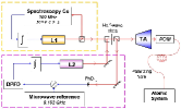
The laser setup consists of two external-cavity laser diodes using SDL 5422 chip. These sources are based on an intracavity wavelength selection by an interference-filter baillard06 and benefit from a narrow linewidth (14 kHz) and a wide tunability (44 GHz). The diodes are regulated around room temperature and supplied by a current of 80 mA to provide an optical output power of 45 mW. The frequency locks are achieved with a feedback to the diode current and the length of the external cavity.
The first laser L1 (Fig. 1), is used as an absolute
frequency reference. It is locked 300 MHz red detuned from the
atomic transition between the and
states of Caesium (D2 line) using a
frequency modulation spectroscopy technique hall81 .
The phase difference between L1 and L2 is locked with the method described in cheinet06 and summarized in the following. Small amounts of light of L1 and L2 are superimposed on a fast photoconductor (PhD12, Hamamatsu G4176, bandwidth: 15 GHz). The beat note at = 9.192 GHz is then mixed with a reference signal, given by a microwave synthesizer yver04 . The output signal is sent to a Digital Phase and Frequency Detector (DPFD, MCH 12140) which derives an error signal proportional to the phase difference between the two lasers. After shaping and filtering, this output signal is used to generate the feedback allowing to phase-lock the laser L2 on L1. In this way, the features of the microwave reference is mapped on the optical signal with a bandwidth of 3.5 MHz.
In order to provide sufficient optical power, the output signals of L1 and L2 are injected with the same linear polarization in a GaAs tapered semiconductor waveguide amplifier (TA, EYP-TPA 0850-01000-3006 CMT03) pumped by a current of = 2 A and stabilized to room temperature. A half-wave plate and a polarizing cube allow the power ratio between the two lasers to be adjusted at the input of the TA. In a normal operation, 11.2 mW of L1 and 16.2 mW of L2 are injected in the TA, which runs in a saturated gain regime. Then the output beam (with a power of 770 mW) passes through an acousto-optical modulator (AOM), driven at 80 MHz, from which the first output order is coupled to a polarizing fibre. This scheme enables the laser light to be pulsed on the atomic system by switching the RF signal of the AOM.
III Self-phase and amplitude modulation
In this part, we study the sideband generation due to simultaneous phase and amplitude modulation in the gain medium. As two closely detuned optical frequencies are injected in the TA, it is crucial to determine the spectral impact of potential non-linear effects in the semiconductor during the amplification process. Indeed, the beat note at 9.192 GHz between L1 and L2 induces a strong modulation of the power through the TA which affects the gain and the optical index in the semiconductor ferrari99 . In this situation, the resulting sidebands could cause undesirable effects on our experiment: for instance detuned excitations can shift the energy levels of our atomic system, called light shift weiss94 , or it could drive unwanted Raman transitions. For this reason, we conducted simulations which were compared to experimental measurements.
The total electric field propagating through the TA can be described by,
where is the wave envelope which varies at the microwave frequency, is the wave vector, and is the optical carrier frequency. By referring to the envelope power ( is its phase), we obtain at the TA input the modulation profile,
| (2) |
where is the nominal modulation power, is the modulation factor and is the phase difference between L1 and L2 (see Appendix A). In our case, we have mW and . The amplifier is then driven between a saturated state and a non-saturated state at the frequency . In order to calculate the sideband generation expected from the amplification process, we write, as for any amplification medium, the interaction between the carriers and the light field equations. This was widely described in reference agrawal89 ; omahony88 for the case of a constant cross section amplifier. Taking into account the amplifier splay (see appendix A), these equations become,
| (3) | |||
| (4) | |||
| (5) |
where is the carrier lifetime in the semiconductor, the saturation energy for the initial amplifier cross section, is the amplifier splay factor, the linewidth enhancement factor and is the wave group velocity. refers to the linear gain and the small-signal gain is defined as,
| (6) |
where and are the current and carrier density required for transparency, the gain coefficient and the confinement factor (see Appendix A).
The sideband generation is due to a phase and an amplitude modulation resulting from a non-linear gain modulation. This gain modulation depends on the field amplitude along the amplifier and lead to a non-linear distortion of the signal at the output of the TA. A modification of the optical index (4) induces an optical phase modulation. Indeed, an increase of the gain modulation exacerbates the phase and the power modulation distortions at the same time.
The evaluation of this effect requires the set of equations (3-5) to be solved. Since the relaxation time and the excitation characteristic time are of the same order of magnitude, the usual adiabatic approximation can’t be used. Therefore, the system has been numerically solved to obtain the steady state electric field at the output of the TA for comparison with experimental measurements.
IV Optical spectrum measurement
Due to the weak power expected in each sideband, usual methods to measure optical spectrum such as the transmission through a Perot-Fabry cavity or the diffraction on a high resolution grating are not suitable. Instead, we use the beat note with a close known optical frequency in order to achieve the precise measurement of the different components of the laser beam. The output signal of a beat note contains a frequency component corresponding to the difference between the two mixed frequencies. It can be measured with a fast photodetector. The power of the beat note is then proportional to the product of the fields of the two components.

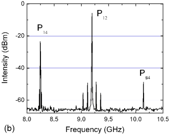
In order to realize a spectrum measurement, we set up a probe laser L4. As shown on Fig. 2, the frequency of L4 can be adjusted around the Cesium D2 line by the comparison to a reference laser L3. This frequency lock is achieved by measuring the beat note of the two lasers, through a Frequency to Voltage Converter (FVC). A reference DC voltage (VC4) allows the frequency detuning between L3 and L4 to be set around 8.6 GHz. As a result, L4 is detuned from L1 by = 8.3 GHz (Fig. 3a). The optical frequency spectrum of the phase-locked lasers (L1+L2) can be analyzed by superimposing the probe beam L4 on the photoconductor PhD12, which exhibits the microwave components of the beat note between L1, L2 and L4. As explained before, mixing three optical frequencies on a photodetector gives rise to three frequencies in the microwave domain. In this setup, L2 and L4 are sufficiently close that the beat note between these two lasers (950 MHz) is filtered out by the detection bandwidth. Thus, we verify that before optical amplification, the microwave spectrum of the PhD12 signal is composed of a component at of power and a component at frequency of power . In order to investigate impact of the amplification on the spectral content, the same beat note is measured again at the output of the polarizing fibre and displayed on Fig. 3b. Compared to the expected microwave spectrum, containing the two previous frequencies ( and ), it exhibits an additional signal at = 10.142 GHz of power which is related to the beat note between L4 and an additional sideband detuned by 9.197 GHz from L2. Another symmetric sideband at 9.192 GHz above L1 leads to a beating signal with L4 out of the bandwidth of detection. Small spurious sidebands around are generated by the acousto-optic modulator (AOM) at 80 MHz and can be ignored in the following.

The TA characterization requires the determination of the set of parameters (). For this purpose, we perform three measurements, which are displayed in Fig. 4. First, we measure as a function of the total optical input power (Fig. 4a). Then we record the two magnitudes and as a function of the total input optical power (Fig. 4b) and the current (Fig. 4c). From , we deduce the ratio between the fields of L1 and the sideband.
Using (Fig. 4a) and (Fig. 4b), we infer m-1, pJ and , which are in agreement with the values indicated in reference agrawal89 . From , we get cm2. Then, we use (Fig. 4c) to work out A and m-3. It gives the active volume m3, in good agreement with the geometrical calculation m3.
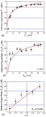
In normal operation, the ratio () of the micro-wave power is of -22 dB, corresponding to an optical power ratio between the sideband and L1 of . As expected, increasing the current or the input power leads to an increase in sideband generation. Finally, we work out from the simulation that the index modulation is responsible for 90 percent of the sideband generation and the amplitude modulation is responsible for the last 10 percent.
V Phase noise measurement
The residual phase noise between the two lasers is crucial for the sensitivity of our experiment. Indeed, the laser phase difference is imprinted on the atom wave-function during the stimulated Raman transitions cheinet08 . The effective phase noise affecting the interferometer is the sum of different contributions: the noise induced by the microwave frequency reference yver04 , the residual noise in the phase-lock loop cheinet06 and the noise added along the propagation through the TA and the fibre. The present study is focused on the characterization of these two last terms.
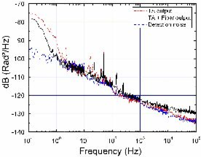
The additional phase noise is measured by mixing the beat notes of the two lasers (L1 and L2) before and after the propagation along the TA and the fibre. The two microwave signals are then amplified and combined together on a mixer (ZMX-10G). Their relative phase is adjusted with a phase-shifter and set around to reach the optimal phase sensitivity at the mixer output. After filtering the high frequency components, the output signal is given by,
| (7) |
where represents the scaling factor (0.3 V/rad) between the phase shift and the output level of the mixer. is the phase noise between the two beat notes. The measurement of the power spectral density of phase noise is obtained with a FFT analyzer and displayed on Fig. 5. It exhibits the phase noise contribution induced by the TA and the fibre. The measurement is compared to the detection noise, which is obtained using the same signal in both inputs of the mixer. This detection noise represents the lower limit of the phase noise which can be detected by this setup. No significant additional phase noise from the TA and the fibre is measured above 1 Hz.
VI Impact on an atom interferometer
Raman transitions enable the manipulation of atomic wave-packets by coupling two internal states of an atom using a two photon transition kasevich91 . In order to drive these transitions, two lasers with a difference of frequency in the microwave range are needed. This laser setup is implemented to realize the functions of mirrors and beam splitters for atoms borde91 in a six-axis inertial sensor canuel06 . A sequence of three optical pulses (, , ) of duration , separated by free propagation time is used to create the equivalent of a Mach-Zehnder interferometer (Fig. 6) for atoms borde02 . Here, we estimate the possible limitations induced by the common amplification of the two Raman lasers in our specific device which come from unwanted Raman transitions due to the sideband generation or additional phase noise in the TA.
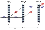
First, the sideband generation in the TA is small enough to not give rise to significant Raman transitions between laser L1 or L2 and one of the sidebands. The diffraction process is characterized by the effective Rabi frequency moler1992 which scales as the product of the fields of the two lasers and the inverse of the Raman detuning. The amplitude of the sideband is 22 dB smaller and 9 GHz further detuned than the main optical fields. Therefore the corresponding Rabi frequency is reduced by almost four orders of magnitude.
Second, we estimate the additional phase shift from the TA. The phase shift at the output of the interferometer is deduced from the transition probability of the atoms between the two coupled states. It depends on the inertial forces and on the the phase noise between the two lasers cheinet08 , as the phase difference between L1 and L2 () is imprinted on the atomic wave function at the moment of each pulse,
| (8) |
The transfer function of the spectral power density phase noise simplifies at low frequency () as,
| (9) |
where , the interaction time, is typically 40 ms. For high frequencies, the transfer function decreases as a second order low pass filter with effective cutoff frequency (). The total phase noise added by the TA and the fibre is given by the integration over the full spectral range of weighted by the transfer function. It leads to fluctuations on the output atomic phase noise of 0.21 mrad from shot to shot. This contribution is negligible compared to the noise generated by the present microwave synthesizer (2.51 mrad), or best frequency synthesizer based on current quartz oscillator ( 1 mrad).
VII Conclusion
To conclude, we demonstrate that amplifying optically carried microwave signal with a tapered amplifier induces neither microwave phase noise nor significant spurious optical sidebands. This setup does not give any additional limitation on the sensitivity of our device, which uses relevant parameters for cold atom interferometer. The sideband generation has been carefully characterized and shows a good agreement with the calculations. This effect becomes more significant as the microwave frequency get smaller. For instance, the model shows that similar results should be found for an interferometer based on Rb atoms (microwave frequency of 6.834 GHz), with an increase of the sideband generation as small as 2 dB.
To a great extent, it shows that a powerful optically carried microwave signal can be realized in two stages: one performing the optical carried microwave signal and the other supplying the optical power. The quality of the amplification does not depend on a particular method to generate the optical signal and should be similar when sideband generation in an electro-optic modulator is used to generate the microwave signal. This can lead to simplifications of optical systems in atom interferometry nyman06 and of amplification for frequency and time dissemination at long distance. In addition, this method could simplify atom interferometer experiments in which several separated powerful Raman beams are required muller08 , as they can be amplified independently without special care. Finally, this study has been realized in the steady state regime, and might be extended to the pulsed regime Takase2007 which allows for higher laser power.
Acknowledgements.
We would like to thank G. Lucas-Leclin for fruitful discussions, E. Foussier for her contribution to the experimental setup, J. D. Pritchard and C. Garrido Alzar for careful readings. We also thank the Institut Francilien pour la Recherche sur les Atomes Froids (IFRAF) and the European Union (FINAQS STREP NEST project contract no 012986 and EuroQUASAR IQS project) for financial support. T.L. thanks the DGA for supporting his work. W.C. thanks IFRAF for supporting his work.Appendix A Light-semiconductor interaction equations
The theory of self phase modulation in semiconductor amplifiers has been developed for pulse propagation in reference agrawal89 to the case where the pulse width is assumed to be much larger than the interband relaxation time ps which governs the dynamics of the induced polarization. Our case concerns the beat note of two lasers, whose frequencies are separated by the beat frequency , and amplified through a tapered semiconductor mm long (7). In reference agrawal89 , it is shown that the dynamic of a semi-conductor with a constant cross section is given by the set of equations,
| (10) | |||
| (11) | |||
| (12) |
In our case, the electric field input is given by,
where the envelope at the amplifier input is given by,
| (14) |
| (15) | |||||
where , , and , and where we set equal to and to .
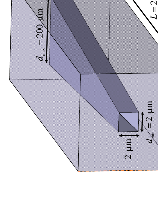
These equations are inferred from a combination of the electromagnetic field propagation equation, on which the slowly varying envelope approximation has been applied, and the carrier density equation. In the latter, the carrier density diffusion has been neglected in the direction (the carrier diffusion length m). However, it tends to make uniform the carrier density in the transverse directions (). The carrier density equation is therefore averaged over the directions and and appears through the factor,
| (16) |
where represents the transverse mode.
In the case of a TA, as the amplifier get larger, the carrier diffusion tends to make the carrier density uniform, which distorts the transverse mode. Nevertheless, since the mode is kept guided, the factor remains of the order of 0.9 and is considered constant in the following. Therefore, the set of equation [10-12] is still valid in the case of a tapered amplifier provided we change the last equation to,
| (17) |
where describes the amplifier splay. It has to be noticed that all losses and dispersion effects have been neglected.
In order to solve the set of equations (10,11,17), we consider the amplifier as a succession of equally long subdivisions of fixed transverse cross section. The combination of equation (17) and equation (10) can be analytically integrated over along each subdivision and then numerically solved according to the shifted time . Afterwards, equation (11) is easily integrated to obtain the electric field . Using a Fourier transform, we compute the electric field spectrum at the TA output.
References
- (1) L. Morvan, N.D. Lai, D. Dolfi, J.-P. Huignard, M. Brunel, F. Bretenaker, A. Le Floch, Appl. Opt. 41, 5702 (2002)
- (2) C. Daussy, O. Lopez, A. Amy-Klein, A. Goncharov, M. Guinet, C. Chardonnet, F. Narbonneau, M. Lours, D. Chambon, S. Bize et al, Phys. Rev. Lett. 94, 203904 (2005)
- (3) R. Wynands and A. Nagel, Appl. Phys. B 68, 1-25 (1999)
- (4) M. Kasevich, and S. Chu, Phys. Rev. Lett. 67, 181 (1991)
- (5) A.J. Seeds, IEEE Trans. Microwave Theory Tech. 50, 877 (2002)
- (6) L. Goldberg, H.F. Taylor, J.F. Weller, and D.M. Bloom, Electron. Lett. 19, 491 (1983)
- (7) F. Kéfélian, R. Gabet, and P. Gallion, Opt. Quantum Electron. 38, 467 (2006)
- (8) G. Santarelli, A. Clairon, S.N. Lea, G. Tino, Opt. Commun. 104, 339 (1994)
- (9) B. Canuel, F. Leduc, D. Holleville, A. Gauguet, J. Fils, A. Virdis, A. Clairon, N. Dimarcq, Ch. J. Bordé, A. Landragin, and P. Bouyer, Phys. Rev. Lett. 97, 010402 (2006)
- (10) G. Ferrari, M.-O. Mewes, F. Schreck, and C. Salomon, Opt. Lett. 24, 151 (1999)
- (11) X. Baillard, A. Gauguet, S. Bize, P. Lemonde, P. Laurent, A. Clairon, and P. Rosenbusch, Opt. Commun. 266, 609 (2006)
- (12) J.L. Hall, L. Hollberg, T. Bear, and H.G. Robinson, Appl. Phys. Lett. 39, 680 (1981)
- (13) P. Cheinet, F. Pereira Dos Santos, T. Petelski, J. Le Gouët, J. Kim, K.T. Therkildsen, A. Clairon, and A. Landragin, Appl. Phys. B 84, 643 (2006)
- (14) F. Yver Leduc, PhD thesis, Université Paris XI (2004)
- (15) D.S. Weiss, B.C. Young, and S. Chu, Appl. Phys. B 59, 217 (1994)
- (16) G.P. Agrawal, and N.A. Olsson, IEEE J. Quant. Electron. 25, 2297 (1989)
- (17) M.J. O’Mahony, J. Lightwave Technol. 6, 531 (1988)
- (18) P. Cheinet, B. Canuel, F. Pereira Dos Santos, A. Gauguet, F. Leduc, and A. Landragin, IEEE Trans. Instrum. Meas. 57, 1141 (2008)
- (19) Ch.J. Bordé, In Laser Spectroscopy X, Singapore, World Scientific, 239 (1991)
- (20) Ch.J. Bordé, Metrologia 39, 435 (2002)
- (21) K. Moler, D.S. Weiss, M. Kasevich, and S. Chu, Phys. Rev. A 45, 342 (1992)
- (22) R.A. Nyman, G. Varoquaux, F. Lienhart, D. Chambon, S. Boussen, J.F. Clément, T. Muller, G. Santarelli, F. P. Dos Santos, A. Clairon, A. Bresson, A. Landragin, and P. Bouyer, Appl. Phys. B 84, 673 (2006)
- (23) T. Müller, M. Gilowski, M. Zaiser, T. Wendrich, W. Ertmer, and E.M. Rasel, Eur. Phys. J. D 53, 273 (2009)
- (24) K. Takase, J. K. Stockton, and M. A. Kasevich, Optics Lett. 32, 2617 (2007)