Bends In Nanotubes Allow Electric Spin Control and Coupling
Abstract
We investigate combined effects of spin-orbit coupling and magnetic field in carbon nanotubes containing one or more bends along their length. We show how bends can be used to provide electrical control of confined spins, while spins confined in straight segments remain insensitive to electric fields. Device geometries that allow general rotation of single spins are presented and analyzed. In addition, capacitive coupling along bends provides coherent spin-spin interaction, including between otherwise disconnected nanotubes, completing a universal set of one- and two-qubit gates.
I Introduction
Electron spins in confined nanostructures show promise as a basis for quantum information processing.Petta2005 ; Nowack2007 ; Hanson2007a ; Pioro-Ladriere2008 Among the realizations of spin qubits, gated carbon nanotubes offer a number of attractive features, including large confinement energy and a nearly nuclear-spin-free environment. A novel circumferential spin-orbit coupling in nanotubes, mediated by s-p hybridization and inversely proportional in strength to the nanotube radius, has been investigated experimentallyKuemmeth2008 ; Churchill2009b and theoreticallyAndo2000 ; Huertas-Hernando2009 ; Chico2009 ; Jeong2009 ; Izumida2009 recently. In this paper, we show that circumferential spin-orbit coupling provides a natural means of creating a strong spatial dependence of the magnitude and direction of the effective magnetic field experienced by a spin qubit formed by confining charge in a nanotube. Along bends in the nanotube, the spin qubit couples efficiently to electrostatic gates, allowing spin control and spin-spin coupling, while along straight regions the spin qubit is insensitive to electric fields and is therefore inactive and protected. Related effects of bending modes on spin relaxation have also been considered recently. Rudner2010
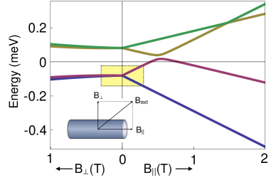
The spin, or quantum two-level system, that forms the physical qubit is a Kramers doublet in a nanotube quantum dot containing an odd number of electrons, in the low-magnetic-field regime. As illustrated in Fig. 1, splitting of these doublets in a magnetic field depends on the direction of the field with respect to the nanotube axis. This is the key observation of our analysis: in tubes with bends, the angle between the tube axis and the applied magnetic field depends on position along the tube. This dependence couples position and spin, allowing electric fields to control spin and create spin-spin coupling. In straight segments, changes in position do not change the angle between the field and the nanotube axis, and so this coupling vanishes. For use as a qubit, relaxation of the low-field Kramers doublet is suppressed due to time-reversal symmetry, in contrast to the qubit formed at the high-field crossingBulaev2008 ; Rudner2010 (at 1.4 T in Fig. 1), consistent with experiment.Churchill2009b
II The Kramers qubit
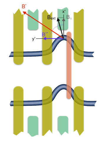
We start by analyzing the spectrum of a quantum dot confined along a bend in a nanotube. The geometry of the system can be described in terms of local (primed) coordinates, , perpendicular to the nanotube axis, and along the nanotube axis (see Fig. 2) at the position of the dot. For bend radius much greater than the interatomic distance, the nanotube band structure is described by that of a locally straight tube,Ando2005 including spin-orbit interaction.Ando2000 ; Huertas-Hernando2009 ; Chico2009 ; Jeong2009 ; Izumida2009 For a nanotube quantum dotBulaev2008 of length , the effective Hamiltonian to leading order in is
| (1) | |||||
where and are Pauli matrices in spin and valley space, respectively, is spin-orbit coupling energy, and is a valley mixing term due to substrate, contacts, gates, or any disorder that breaks the crystal symmetry. The first two terms describe the two Kramers doublets, while the last term describes the coupling to magnetic fields of spin and orbital moments. Note that orbital moments are always along the nanotube axis unit vector . We consider only planar devices with magnetic fields applied in plane of the bent nanotube, but this restriction can be readily generalized to bends and fields out of the plane.
The magnetic field dependence of a nanotube quantum dot, including effects of spin-orbit coupling, is shown in Fig. 1 for typical parameters for small-gap semiconducting nanotubes. Two parameters characterizing the nanotube device are the spin-orbit energy scale, , and , which characterizes the mixing of and valleys due to disorder on length scales comparable to or smaller than the nanotube radius, . Fourfold degeneracy at zero applied field, , is lifted by , typically meV, giving two doublets that are well separated at low temperatures. Either doublet may constitute a qubit in the present scheme, depending on occupancy of the dot. Here, we concentrate on the lower pair, appropriate for a single confined electron, in the low-field regime (boxed region in Fig. 1), away from the anticrossing of different orbital states.
Diagonalizing the above 4 Hamiltonian and projecting onto the lowest two eigenstates yields an effective spin-1/2 system, which is our qubit. It has an anisotropic g factor described by the Hamiltonian
| (2) |
where are Pauli matrices, is the Bohr magneton, and is the gyromagnetic tensor. In terms of local nanotube coordinates,
| (3) |
where and refer to components of the vectors in Eq. (3) along and , respectively. Components of can be expressed in terms of nanotube parameters,
| (4) | |||||
| (5) |
where is the spin g factor and is the orbital g factor, with for typical nanotubes. We emphasize that because the coordinates are local, changes in confinement position along a bend will change the directions and magnitudes of field components and for fixed external field. Eqs. (4) and (5) show how spatial inhomogeneity in can also couple spin to position. When this inhomogeneity is small compared to either or this effect is weak.
We introduce the effective field, , felt by an electron spin, including spin-orbit effects, as a function of position along the nanotube. Variation in the magnitude and direction of along a bend are shown in Fig. 2 for realistic device parameters.
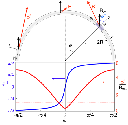
Because the tensor in local coordinates, , is diagonal, the effective field is found by , where is the matrix that rotates to the local nanotube coordinates. The effective field is
| (6) | |||||
This formula forms the basis for the discussion in Figs. 2 and 4.
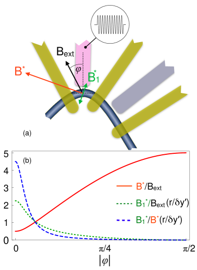
III Electric dipole spin resonance
The sizable variation of along the bend suggests several applications that involve both finite and infinitesimal gate-induced motion. As a first example, we consider electric dipole spin resonance (EDSR) using an oscillating gate voltage, as illustrated in Fig. 3. We consider a single electron confined by gates to a region containing a bend. A second electron confined in an adjacent dot may be used to detect spin rotation via Pauli blockade.Hanson2007a An external field is applied at an angle to the local transverse () direction, and a gate voltage, oscillating at frequency , causes the center position of the dot to move by an amount . This motion modifies the orbital coupling to the applied field, while Zeeman coupling is unchanged. Small displacements of the dot position then result in a perturbation of the Hamiltonian (1). Only the tangent vector in (1) depends on , with derivative . Again projecting onto the lowest Kramers doublet, the modulation of the effective field becomes , where
| (7) |
and
| (8) |
Therefore the oscillatory part of the effective field points along the nanotube axis, , which in general is not aligned with , but has components both along , with magnitude , and transverse to , with magnitude , given by
| (9) | ||||
| (10) |
where . For a reasonable nanotube bend radius, m, and gate-induced dot motion, nm, the plots in Fig. 3 indicate a transverse field of order T for mT, an applied field for which the qubit remains well defined (Fig. 1). At the resonance frequency, ( is Planck’s constant), the electron spin will precess at the Rabi frequency, , which exceeds several MHz.
Note from Eq. (10) that the transverse oscillating field, , vanishes in the absence of valley mixing. For weak valley mixing, , the maximal ratio is obtained at , i.e., when the applied field is transverse to tube.
Cross coupling of ac gate voltages to dots in nearby straight regions of the nanotube (as in the example in Fig. 3) will not effect spins there. Moreover, adjacent dots also in bent regions (with the same or different ) will have different resonant frequencies— depends on position along a bend—and so will be relatively insensitive to the oscillating gate.
This example illustrates how modest bends and ac gate voltages are capable of generating efficient and selective spin rotation with transverse field strengths comparable to existing few-spin EDSR schemes.Golovach2006 ; Nowack2007 ; Laird2007 ; Pioro-Ladriere2008
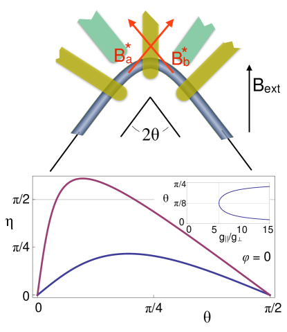
IV Fast spin rotation via non-adiabatic passage through bends
As a second example of spin manipulation, we consider the geometry in Fig. 4(a), consisting of two straight segments on either side of a single bend, with radius of curvature , forming an angle . Two quantum dots, denoted and , are defined by gates on the straight segments of this “coat hanger” shape, and the external field is applied in the plane, at an angle with respect to the symmetry axis. Effective fields and in the two dots differ in both magnitude and direction. In particular, the angle between and , given by
| (11) |
can reach for realistic device parameters. Fig. 4(b) shows as a function of bend angle, , for two values of g-factor anisotropy, , one that does and one that does not exceed the critical value, , above which the condition can be met for two values of . In particular, typical nanotubes, with , easily allow this orthogonality condition.
The coat hanger geometry provides nonresonant qubit rotation when an electron is moved nonadiabatically from one dot to the other. Because the precession field is the same order as the quantizing field, precession rates, , are typically two to three orders of magnitude faster than the EDSR device described above, allowing nanosecond rotations. As an example, for and , a qubit initialized in dot and moved nonadiabatically to dot will rapidly precess around , at a frequency . At some point along the passage, will be purely transverse to the nanotube axis. At this point, the condition for nonadiabatic passage becomes very liberal, only requiring a passage rate faster than . From Eq. (5), , which makes the minimum gap small. Experimental values eV and eV give . Using mT allows pulse transition occurring in under 10 ns to be considered nonadiabatic, a criterion that is readily achieved with standard arbitrary waveform generators and coaxial cryogenic wiring.
A notable feature of the coat hanger geometry is that the electron spends nearly all of its time—including during rotation—in straight regions of the tube, where stray electric fields do not cause inadvertent qubit rotation; only during the brief non-adiabatic passage from one straight region to another is the qubit on a bend and therefore sensitive to decoherence due to electrical noise. A single bend (as in Fig. 4a) allows spin rotation around a single axis. A nanotube with two bends (for instance, in the shape of the letter N) allows rotation around two axes, and thus arbitrary qubit rotation.
V Spin-spin interaction via capacitative coupling
The coupling of spin and position also provides a natural mechanism for spin-spin interaction using a capacitive gates or resonant cavities.Flindt2006 ; Trif2007 This allows nonlocal two-qubit interaction in a single nanotube by coupling adjacent or non-adjacent qubits using gates between multiple bends, as well as providing two-qubit interaction between different nanotubes. Coherent coupling of spins in different nanotubes using gated bends solves an important challenge of nanotube-based quantum information systems of how to move quantum information through networks or arrays of multiple tubes.
Previous work has demonstrated capacitive coupling between separated quantum dots on the same nanotube,Churchill2009b as well as between two quantum dots on different Si/Ge nanowires,Hu2007 and between a nanotube quantum dot and a single-electron transistor,Biercuk2006 all over distance scales of m. The coupling between dots is mediated by a relatively large metallic gate whose self-capacitance typically exceeds the self-capacitances and of the dots. In this configuration (see Fig. 5), the electrostatic interaction energy, , is approximately given by where and are the mutual capacitances of the dots to the coupling gate. Typical values from previous experiments give , where is the Coulomb charging energy of the individual nanotube dots, typically 5 meV.
The two-qubit Hamiltonian is , where and are the single dot Hamiltonians as in Eq. (1), and where the interaction term, , depends on the position of the electrons within the two dots. For small displacements, the linear terms of are
| (12) |
where is the field defined in (7) for dot . To second order in the dot displacements, the spin interaction becomes
| (13) |
where
| (14) |
Inserting Eq. (7) into Eq. (13) leads to
| (15) |
with
| (16) |
for identical parabolic confinement potentials. It has the expected dependences on g-factor anisotropy and radii of curvature of the two bends, and . It also depends on the sensitivity of to differential motion along the nanotubes, and . In this expression is the effective electron mass and is the characteristic level spacing in the two quantum dots, which together characterize the stiffness of the confining potential to spin-dependent forces.
This form, with parallel spin component coupled to transverse applied field components is a consequence of locally circular motion along the bends, where changes in field components (which quantize the spin direction) upon infinitesimal motion are transverse to the field components themselves. Expressing in terms of the fields (Fig. 5) yields a transverse-Ising-like form, which is known to generate spin entanglement between the coupled dots. Two applications of such a gate in combination with single qubit rotations generates a CNOT gate and therefore, together with general single-qubit rotations, constitutes a universal gate set.Barenco1995
Realistic values for can be estimated by noting that the dependence of on and , reflects the dependence of mutual capacitances and on dot motion. The characteristic scale of this geometrical dependence is the dot length, , giving the estimate
| (17) |
The stiffness, characterizing changes in dot position in response to spin-dependent electrostatic forces, can similarly be estimated by replacing the oscillator length with the dot length , giving
| (18) |
Using representative experimental values for coupling strength eV, g-factor anisotropy , level spacing meV, and dot size m, and taking reasonable values for bend radii m, yields the estimate eV/T2. For applied fields of 100 mT, this strength of coupling allows two-qubit operations on time scales of s, which is considerably faster than the anticipated coherence time (which, however, has not yet been measured). Gate operation time can likely be reduced further by decreasing , bend radii, or level spacing.
VI Conclusions
In summary, the combination of spin-orbit coupling and curved geometryBelov2005 allows qubit novel control schemes using electric gate manipulation. Notwithstanding the ability to control spin using electric fields in nanotubes with bends, spins confined to straight regions of the nanotube electrons are immune to electrical noise. Bends also allow spin-spin interaction between capacitively coupled nanotubes, providing an entangling transverse-Ising-like two-qubit gate, which along with full single-qubit rotations, provided by nanotubes with two bends, constitutes a universal set of gates.
Various methods for creating nanotubes with bends have been demonstrated. These include growth techniques that yield serpentine nanotubes with multiple bendsGeblinger2008 and manipulation, for instance using an atomic-force microscope,Postma2001 ; Bozovic2001 ; Biercuk2004 following growth.
Acknowledgements.
We thank H. Churchill, P. Herring, F. Kuemmeth, D. Loss, J. Paaske, E. Rashba, A. Sørensen and J. Taylor for discussions. This work was supported in part by the National Science Foundation under grant no. NIRT 0210736, NRI-INDEX, US Department of Defense, and The Danish Council for Independent Research Natural Science (FNU).References
- (1) J. R. Petta et al., Science 309, 2180 (2005).
- (2) K. C. Nowack, F. H. L. Koppens, Y. V. Nazarov, and L. M. K. Vandersypen, Science 318, 1430 (2007).
- (3) R. Hanson, J. R. Petta, S. Tarucha, and L. M. K. Vandersypen, Rev. Mod. Phys. 79, 1217 (2007).
- (4) M. Pioro-Ladrière et al., Nature Physics 4, 776 (2008).
- (5) F. Kuemmeth, S. Ilani, D. C. Ralph, and P. L. McEuen, Nature 452, 448 (2008).
- (6) H. O. H. Churchill et al., Phys. Rev. Lett. 102, 166802 (2009).
- (7) T. Ando, J. Phys. Soc. Jpn. 69, 1757 (2000).
- (8) D. Huertas-Hernando, F. Guinea, and A. Brataas, Phys. Rev. Lett. 103, 146801 (2009).
- (9) L. Chico, M. P. López-Sancho, and M. C. Muñoz, Phys. Rev. B 79, 235423 (2009).
- (10) J.-S. Jeong and H.-W. Lee, Phys. Rev. B 80, 075409 (2009).
- (11) W. Izumida, K. Sato, and R. Saito, J. Phys. Soc. Jpn. 78, 074707 (2009).
- (12) M. Rudner and E. I. Rashba, arxiv.org/abs/1001.4306.
- (13) D. V. Bulaev, B. Trauzettel, and D. Loss, Phys. Rev. B 77, 235301 (2008).
- (14) T. Ando, J. Phys. Soc. Jpn. 74, 777 (2005).
- (15) V. N. Golovach, M. Borhani, and D. Loss, Phys. Rev. B 74, 165319 (2006).
- (16) E. Laird et al., Phys. Rev. Lett. 99, 246601 (2007).
- (17) C. Flindt, A. S. Sørensen, and K. Flensberg, Phys. Rev. Lett. 97, 240501 (2006).
- (18) M. Trif, V. N. Golovach, and D. Loss, Phys. Rev. B 75, 085307 (2007).
- (19) Y. Hu et al., Nature Nanotechnology 2, 622 (2007).
- (20) M. J. Biercuk et al., Physical Review B 73, 201402(R) (2006).
- (21) A. Barenco et al., Phys. Rev. A 52, 3457 (1995).
- (22) V. V. Belov, S. Y. Dobrokhotov, V. P. Maslov, and T. Y. Tudorovskii, Physics-Uspekhi 48, 962 (2005).
- (23) N. Geblinger, A. Ismach, and E. Joselevich, Nature Nanotechnology 3, 195 (2008).
- (24) H. W. C. Postma et al., Science 293, 76 (2001).
- (25) D. Bozovic et al., App. Phys. Lett. 78, 3693 (2001).
- (26) M. J. Biercuk, N. Mason, J. M. Chow, and C. M. Marcus, Nano Letters 4, 2499 (2004).