Observation of Raman -band splitting in top-doped few-layer graphene
Abstract
An experimental study of Raman scattering in -layer graphene as a function of the top layer doping is reported. At high doping level, achieved by a CHF3 plasma treatment, we observe a splitting of the band in the spectra of bilayer and 4-layer graphene ( even), whereas the splitting is not visible in case of monolayer and trilayer graphene ( odd). The different behaviors are related to distinct electron-phonon interactions, which are affected by symmetry breaking and Fermi level position in different ways in the various -layer graphenes. In trilayer graphene, a weakening of the electron-phonon coupling as a function of the Fermi energy induces a hardening of all zone-center in-plane optical phonon modes, like in monolayer graphene. On the other hand, in 4-layer graphene two distinct trends are observed in the band as a function of doping, suggesting the presence of two different groups of electron-phonon interactions, like in bilayer graphene.
I Introduction
Since the demonstration of the isolation of a single atomic plane of graphite (graphene) on a standard substrate Novoselov2005 , it has suddenly become possible to experimentally verify many theoretical predictions about the peculiar physical behavior of graphene-based systems. Indeed, the linear dispersion curves, and the consequent relativistic-like behavior of charge carriers in monolayer graphene, have been broadly confirmed by several experimental observations CastroNeto2009 ; Geim2007 . Interestingly, stacking a number of graphene layers on top of each other can lead to new physical systems exhibiting completely different properties. For instance, some peculiar gate-tunable electronic and optical properties have been recently reported in the bilayer case Zhang2009 ; Mak2009b ; Kuzmenko2009 ; Tang2010 .
In fact, the interlayer coupling induces a gradual departure from the electronic bands of monolayer graphene Koshino2009 , until the bulk limit (graphite) is reached for large enough. Therefore, there is a range of where the physical properties of graphene stacks are sensitive even to a variation . For instance, a qualitative difference between the transport properties of bilayer and trilayer graphene was evidenced in recent experiments Craciun2009 . Moreover, the optical absorption spectra are predicted to systematically vary with the layers number within the effective mass approximation for Koshino2009 , reflecting the gradual modification of the band structure. Here we show that a clear splitting of the Raman band is observed for and , when the multilayer graphene symmetry is broken by heavy doping of the top layer, whereas the splitting is not observed for and . The presence or absence of splitting highlights different electron-phonon interactions, which are influenced by doping and symmetry breaking in distinct ways in the various -layer graphenes. The reported results confirm two experimental reports in literature about the band splitting in bilayer graphene (obtained by gate field effect) Malard2008 ; Yan2009 , adding new important information such as a systematic study of the splitting as a function of the layers number and of the doping.
Raman spectroscopy is a very powerful tool for studying graphene, yielding information on the electronic structure and on the electron-phonon coupling (EPC) in the material Ferrari2007 ; Malard2009 . In fact, this technique allows to clearly distinguish a monolayer and a bilayer from a few-layer graphene, through the analysis of the band Ferrari2006 , and to estimate the charge carrier density and type in monolayer graphene from the spectral positions and relative intensities of the and bands Das2008 . The band (at cm-1) is due to a first-order Raman scattering process involving zone-center in-plane optical phonons. In stacked graphene layers, the vibrations in different atomic planes can combine with each other in various ways, depending on the number of layers and on the stacking order. Moreover, the EPC is affected by the number and symmetry of the stacked layers, so that the band may be used to study the effects of symmetry breaking and doping on the electronic and phononic properties of multilayer graphenes. The knowledge of these effects is of fundamental importance for the development of graphene-based field-effect electronic devices.
II Experimental
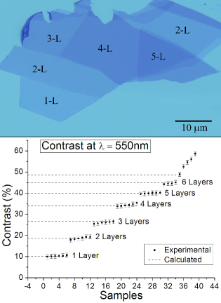
Graphene layers studied in this work were deposited on a 285 nm thick on substrates, by adhesive tape exfoliation of natural graphite. Then, the samples were analyzed by optical microscopy, in order to estimate the number of graphene layers composing the deposited thin flakes. It can be seen in Fig. 1 that the contrast (defined as , where and are the reflected light intensities from the substrate with and without graphene, respectively) measured on many semi-transparent flakes increases in a stepwise manner. The analysis of the Raman band confirmed that the lowest two steps correspond to monolayer and bilayer graphenes, indicating that few graphene layers can be counted by contrast analysis. Such a behavior is related to the optical absorption of graphene, which was found to be directly proportional to the number of layers for small enough Nair2008 . Using appropriate filters in order to select the wavelengths at which the contrast variation is high, we were able to distinguish up to 6 layers. Moreover, the experimental contrast values were checked by theoretical calculations within the Fresnel coefficients approach Bruna2009 .
After a preliminary annealing in vacuum (1x10⁻⁵ mbar for two days) in order to remove possible adsorbed impurities from the graphene surface, the first run of Raman measurements was carried out. Raman spectra were acquired by means of a Jobin-Yvon U1000 Raman spectrometer equipped with a microscope (100X objective) and with an Ar-Kr laser, using the excitation wavelength = 514.5 nm. The incident laser power focused on the sample was adjusted to be less than 5 mW, to avoid any local heating effect. Various -layer graphene flakes were analyzed, displaying the standard and bands reported in literature.The band at 1350 cm-1, related to lattice defects, was never observed in the experiments, confirming the good quality of our graphene samples. Moreover, the analysis of the monolayer spectra ( peak at 1582 cm-1 with FWHM 13 cm-1) indicates that the unintentional doping level in the pristine samples was relatively low (about 1X1012 cm-2) Pisana2007 .
Then, the samples were subjected to a radio frequency (RF) plasma treatment in CHF3 gas, and immediately (within a few minutes) re-characterized by Raman spectroscopy.
III Results and Discussion
III.1 CHF3 plasma
Previous studies reported in literature Tachibana1999 ; Hancock2001 have shown that the following radical species can be found in a CHF3 plasma: atoms and () radicals. In dry etching processes, atoms normally act as the reactive species (responsible for the etching), whereas radicals are passivation precursors giving rise to polymer deposition. It has been observed that, in the case of CHF3 plasma processes, the etch rate decreases with increasing flow (in contrast with what happens in the case of CF4 plasma), due to the low concentration ratio Choi2008 . This means that the action of atoms becomes more effective with decreasing the flow rate, because the passivating action of radicals is reduced. In our experiments, we have observed an increasing modification of the graphene Raman spectra, with decreasing the flow rate in the plasma treatment.
In particular, we performed a preliminary study on monolayer graphene processed at various CHF3 flow rates. Fig. 2 shows that the plasma treatment induces a blue shift of both and peaks, which increases with decreasing the gas flow. Moreover, below a flow rate threshold (about 6 SCCM), two new peaks arise at about 1350 cm-1 ( peak) and 1620 cm-1 ( peak), which indicate the presence of defects in the lattice. Also the effect on the Raman spectra of -layer graphenes, which is going to be discussed in detail in the following Section, was remarkably reduced with increasing the gas flow rate.
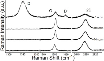
In analogy with the mechanism involved in the etching processes, the interaction of atoms with the graphene surface is likely reduced at high flow rate, because of the passivating action of the radicals. Therefore, the effect of CHF3 plasma on graphene Raman spectra can be ascribed to the adsorption of atoms on the surface. With increasing the coverage, the modification of the graphene properties becomes more important, passing from a p-type doping effect (blue-shifted and peaks) Das2008 to a structural modification ( and peaks) at a very low flow rate (less than 6 SCCM). The doping effect can be ascribed to an electron transfer from graphene to adsorbed atoms, i.e. a mechanism analogous to the observed charge transfer between graphene and adsorbed atoms Ohta2006 . At very low gas flow, when the passivating action of the radicals is minimized, chemical modification (fluorination) of graphene may eventually occur, with a transition from to hybridization similar to that observed in graphane formation by plasma hydrogenation Elias2009 . This evolution may be analogous to the transition from semi-ionic to covalent bonding observed in carbon nanotubes treated in plasma Plank2003 .
Here, we discuss the results of processes carried out at a gas flow of 6 SCCM (pressure of 100 mTorr) for 5 minutes, at RF power = 15 W. Such experimental conditions lead to a very high doping, without structural modification of the graphenes. Moreover, the symmetry of stacked graphenes is broken by the dipole moment generated by the charge transfer from graphene to the adsorbed atoms. Therefore, the situation under study is very similar to that found in field-effect experiments, and the results here reported may be useful for the study of gated graphene-based devices.
III.2 band splitting and electron-phonon coupling in -layer graphene
We focus now on the effect of top doping on the Raman band, which displays very distinct features depending on the number of stacked graphene layers. The change of the band induced by plasma treatment in the various cases is visible in Fig. 3, where the spectra at and were acquired on the same substrate before and immediately after the treatment, respectively. The peak of monolayer graphene is largely blue-shifted (to 1590 cm-1) and narrowed (FWHM 6 cm-1). Both the observations are consistent with an increase of the doping level, which induces a hardening of the mode, due to the non-adiabatic removal of a Kohn anomaly for zone center optical phonons Lazzeri2006 , and a reduction of the linewidth, due to Pauli exclusion principle which inhibits phonon decay into electron-hole pairs when the Fermi level surpasses half the phonon energy Yan2007 . On the other hand, the bilayer and 4-layer spectra display a very evident splitting of the -mode, whereas the behavior of trilayer spectrum is similar to that of monolayer. These results have been confirmed on different flakes on the same sample and on different samples.
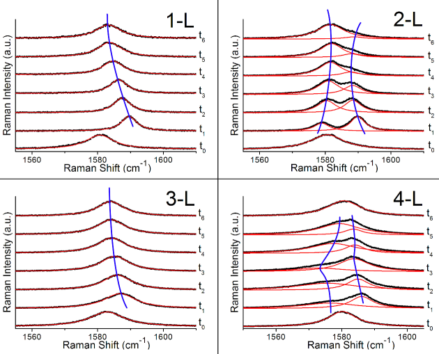
Furthermore, we observed that the modification induced by the plasma treatment was not stable under ambient conditions, as the Raman spectra changed with the passing of time, slowly tending to their pristine form (Fig. 3). Indeed, the initial condition can be restored by a vacuum annealing, so that the plasma treatment can be repeated for several times in a reproducible way. Such a reversible behavior is consistent with the absence of the peak, which indicates the lack of structural modification of the material (in contrast with the case of the chemical modification obtained by plasma treatment at very low gas flow). As previously discussed, the monolayer spectra, showing the hardening of both the -mode and the mode, tell us that a strong -type doping is achieved Das2008 upon plasma processing. Therefore, we were able to gradually vary the doping level on top of each -layer graphene, studying the effect for different values of .
The effect of charged adsorbates has already been studied on epitaxial bilayer graphene on SiC by ARPES measurements Ohta2006 . It was shown that the electronic bands of bilayer graphene are strongly affected by a potassium atoms coverage on the top surface, due to the -type doping induced by the adsorbates. Indeed, because of the short screening length along the -axis of stacked graphenes Ohta2007 , the majority of the doping charge is localized in the top layer and a dipole moment is formed, giving rise to a symmetry breaking and to the consequent band gap opening McCann2006 . In our case, an analogous effect is likely to occur: the doping charge density rapidly decreases going from the top layer to the bottom, thus altering the symmetry of the multilayers. The symmetry breaking can affect very much the physical properties of the system, as it eliminates the symmetry constraints which rule both phonon Raman activity and EPC. In these conditions, all phonon modes included in the band can become Raman active and strongly mixed with each other Ando2009 , and the EPC is affected by the modification of the electronic bands.
In Fig. 3, the band dependence on the doping is visible in all cases, but it looks different for different values. An estimation of the doping level may be obtained from monolayer graphene spectra, basing on the peak position and linewidth, and on the intensity ratio of the and peaks Das2008 , but we have verified that different monolayers can display slightly different peak positions on the same sample, due to the difficulty of controlling the native doping of graphene in ambient atmosphere Casiraghi2007 . Furthermore, monolayer graphene is likely to have a different reactivity with respect to that of few-layer graphene, as experimentally observed in the case of hydrogenation Elias2009 ; Ryu2008 . Also in our experiments, we have seen that, after plasma treatment at very low flow rate, the peak is hardly observed in the few-layers spectra, whereas the monolayer spectrum displays a very evident peak. Therefore, it seems not correct to extrapolate the doping values from the monolayer analysis to interpret the few-layer spectra. However, although a precise quantitative estimate of carrier concentration in each case is not possible in our experiments, we can monitor the different behavior of -layer graphene Raman spectra with decreasing the top doping, starting from high doping levels (more than ) as suggested by the analysis of monolayers spectra.
The effect in the bilayer can be interpreted on the basis of some recent literature. Indeed, the splitting of the Raman band was recently observed in gated bilayer graphene Malard2008 , and ascribed to the inversion symmetry breaking induced by the gate field effect and to two distinct EPC involved in the band. This is due to the fact that the band of bilayer graphene includes two doubly degenerate modes, and , which are symmetric and antisymmetric with respect to the inversion symmetry, respectively. Consequently, only the mode is normally Raman active, unless inversion symmetry breaking switches the mode on, too. It has been shown by Ando and Koshino Ando2009 that, in the presence of asymmetry in the potential of the two stacked layers, symmetric and antisymmetric modes are strongly mixed with each other and two peaks appear in the Raman spectrum. Moreover, phonons can be considerably modified by resonant electronic interband transitions, when the asymmetry opens up a gap comparable to the phonon energy. Ab initio calculations have been performed to compute the band of bilayer graphene in asymmetric conditions as a function of the carrier concentration in the top and bottom layer ( and ) Gava2009 , predicting the behavior of the two modes which become Raman visible at certain values of and .
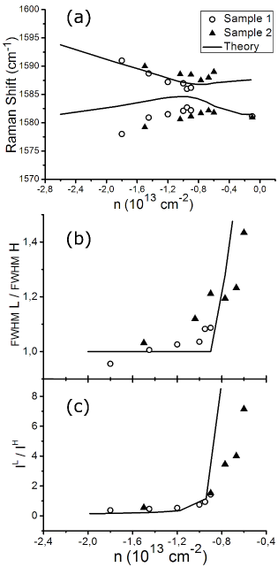
In Fig. 4, we report the analysis of the two Lorentzian peaks which can fit the bilayer band at various stages of the plasma modification, for two different samples. The experimental evolution of the peaks position has been fitted by the theoretical curves obtained from ref. Gava2009 , assuming that about the of the total charge carriers is confined in the top layer, according to ref. Ohta2007 , and using the total carrier concentration as the free parameter in the fitting. Then, the other spectral features (intensity and linewidth) have been compared to the behavior predicted in ref. Gava2009 , considering the carrier concentration values obtained from the best fit of the peaks position curve. It can be seen that a good qualitative agreement is obtained for all the analyzed parameters. In particular, the threshold at about , after which a steep variation of both the intensity and linewidth ratios is predicted by theory, is well reproduced by the experimental data, thus confirming the consistence of the carrier concentration results obtained by fitting the peaks position curves. Therefore, the behavior of the bilayer band is well interpreted in the framework of an asymmetric carrier distribution model.
In order to interpret the spectra for , it is worth to consider, first of all, the evolution of the band with as predicted by group theory. Indeed, applying the group theory to Bernal stacked graphene layers, the irreducible representations of the infrared and Raman active modes at the point for -layer graphene can be obtained Jiang2008 ; Malard2009b , as listed in Table 1. The modes related to the band are the , , and in-plane modes, while the modes are related to out-of-plane phonons.
| Even | ||
|---|---|---|
| Odd |
and modes are found in case of inversion symmetry of the system ( even), whereas and modes appear for mirror symmetry ( odd). Importantly, only the inversion symmetry inhibits the Raman activity of antisymmetric modes. It can be obtained by ab initio calculations Saha2008 that in trilayer graphene two modes and one mode can be found at the G-band frequencies, whereas in 4-layer graphene two modes and two modes vibrate at the band frequencies. The inversion symmetry breaking, produced by the top doping, switches on the previously Raman silent antisymmetric modes in even-layer graphene, so that all the phonon modes become Raman active and mixed in -layer graphene for every value. Moreover, like in the bilayer case previously discussed, the EPC can be strongly affected by the lack of symmetry constraints and by the change of the electronic band structures.
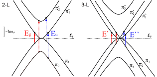
The absence of splitting for trilayer graphene can be qualitatively interpreted considering the allowed electronic interband transitions which give rise to the phonon energy renormalization (Kohn anomaly) when (low doping). In Fig. 5 it is shown that both and phonons can couple with electronic transitions when the Fermi level is at the Dirac point, whereas in bilayer graphene only the symmetric mode can efficiently create electron - hole pairs, due to energy conservation and symmetry selection rules. Indeed, first principles calculations Yan2009b have shown that in trilayer graphene the phonon linewidths of symmetric and antisymmetric modes are all of the same order of magnitude, whereas in the bilayer the antisymmetric linewidth is two orders of magnitude smaller than that of the symmetric mode. Therefore, almost the same EPC strength is expected for the three phonon modes in trilayer graphene, giving rise to the phonon energy renormalization at and to the consequent hardening of all phonons with moving the Fermi level, like in monolayer graphene. This is a qualitative different case with respect to that of bilayer, where only the symmetric phonon energy is renormalized at . The presence or absence of the band splitting in the two cases reflects the presence or absence of distinct EPC for phonons of distinct symmetry.
The observation of splitting in the 4-layer spectrum suggests the presence of distinct EPC for the different phonon modes in analogy with the bi-layer behavior. In Fig. 6 we show the experimental position of the two lorentzian peaks fitting the 4-layer band, as a function of doping as obtained from the bilayer analysis. It is worth noting that a minimum can be clearly identified in the curve of the low frequency peak, indicating that a maximum is likely to occur in the EPC for some phonon modes at a given doping value ().
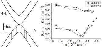
Such a feature can be interpreted by taking into account the band structure of the 4-layer, which can be approximated by two bilayer type band structures Koshino2009 . In particular, intraband transitions occurring between two sub-bands separated by , which corresponds to an experimentally observed absorption by IR spectroscopy Mak2009 , may give rise to an almost resonant coupling with phonons (), and to a consequently strong renormalization of phonon energy. This EPC is expected to have a maximum when the Fermi level reaches the high energy sub-band (see Fig. 6), when the number of possible intraband transitions is maximized. Therefore, the doping value , at which a minimum for the Raman peak position is observed, is likely to correspond to the Fermi energy touching the high energy sub-band at . A theoretical analysis of the 4-layer band structure and density of states in the presence of asymmetric doping may confirm this hypothesis.
IV Conclusions
In summary, we have experimentally investigated the Raman band for -layer graphene () in the presence of high asymmetric doping, finding two different types of behavior. For odd, the band is always fitted by a single lorentzian peak, which is blue-shifted with increasing the doping level. This is due to a strong EPC for all phonon modes when , which decreases with increasing the Fermi energy. On the other hand, for even, an evident splitting of the band is observed, related to the presence of distinct EPC for phonons of distinct symmetry. In particular, in the 4-layer case a signature of the van Hove singularity at is likely to be observed as a minimum of the low energy peak position.
Insights into the electron - phonon interactions in - layer graphenes in the presence of top doping can be useful for the study of field effect graphene-based devices. Moreover, the plasma treatment may be a powerful technique for the study of graphene in the presence of a coverage of highly electronegative atoms such as fluorine.
Finally, the variety of the results reported in the literature about the Raman band in heavily doped bilayer graphene Malard2008 ; Yan2008 ; Yan2009 ; Das2009 suggests that the repartition of the additional charge carriers is not well understood in most experiments. Therefore, suspended graphene samples may be a good testbed to further investigate the distribution of the doping, especially in the bilayer case. Berciaud2009 ; Ni2009
V acknowledgments
This work was carried out within the EURAMET Joint Research Project ”ULQHE”. The research within this EURAMET JRP receives funding from the EC FP7, ERA-NET Plus, under Grant Agreement No. 217257.
References
- (1) K. S. Novoselov, D. Jiang, F. Schedin, T. J. Booth, V. V. Khotkevich, S. V. Morozov, and A. K. Geim, Proc. Natl. Acad. Sci. U.S.A. 102, 10451 (2005).
- (2) A. H. Castro Neto, F. Guinea, N. M. R. Peres, K. S. Novoselov, and A. K. Geim, Rev. Mod. Phys. 81, 109 (2009).
- (3) A. K. Geim, and K. S. Novoselov, Nat. Mater. 6, 183 (2007).
- (4) Y. Zhang, T. T. Tang, C. Girit, Z. Hao, M. C. Martin, A. Zettl, M. F. Crommie, Y. R. Shen, and F. Wang, Nature (London) 459, 820 (2009).
- (5) K. F. Mak, C. H. Lui, J. Shan, and T. F. Heinz, Phys. Rev. Lett.) 102, 256405 (2009).
- (6) A. B. Kuzmenko, L. Benfatto, E. Cappelluti, I. Crassee, D. van der Marel, P. Blake, K. S. Novoselov, and A. K. Geim, Phys. Rev. Lett.) 103, 116804 (2009).
- (7) T. T. Tang, Y. Zhang, C. H. Park, B. Geng, C. Girit, Z. Hao, M. C. Martin, A. Zettl, M. F. Crommie, S. G. Louie, Y. R. Shen, and F. Wang, Nat. Nanotechnol.) 5, 32 (2010).
- (8) M. Koshino, and T. Ando, Solid State Commun. 149, 1123 (2009).
- (9) M. F. Craciun, S. Russo, M. Yamamoto, J. B. Oostinga, A. F. Morpurgo, and S. Tarucha, Nat. Nanotechnol. 4, 383 (2009).
- (10) L. M. Malard, D. C. Elias, E. S. Alves, and M. A. Pimenta, Phys. Rev. Lett. 101, 257401 (2008).
- (11) J. Yan, T. Villarson, E. A. Henriksen, P. Kim, and A. Pinczuk, Phys. Rev. B 80, 241417(R) (2009).
- (12) A. C. Ferrari, Solid State Commun. 143, 47 (2007).
- (13) L. M. Malard, M. A. Pimenta, G. Dresselhaus, and M. S. Dresselhaus, Physics Reports 473, 51 (2009).
- (14) A. C. Ferrari J. C. Meyer, C. Casiraghi, M. Lazzeri, F. Mauri, S. Piscanec, D. Jiang, K. S. Novoselov, S. Roth, and A. K. Geim, Phys. Rev. Lett. 97, 187401 (2006).
- (15) A. Das S. Pisana, B. Chakraborty, S. Piscanec, S. K. Saha, U. V. Waghmare, K. S. Novoselov, H. N. Krishnamurthy, A. K. Geim, A. C. Ferrari and A. K. Soo, Nat. Nanotechnol. 3, 210 (2008).
- (16) R. R. Nair, P. Blake, A. N. Grigorenko, K. S. Novoselov, T. J. Booth, T. Stauber, N. M. R. Peres, and A. K. Geim, Science 320, 1308 (2008).
- (17) M. Bruna, and S. Borini, Appl. Phys. Lett. 94, 031901 (2009).
- (18) S. Pisana, M. Lazzeri, C. Casiraghi, K. S. Novoselov, A. K. Geim, A. C. Ferrari and F. Mauri, Nat. Mater. 6, 198 (2007).
- (19) K. Tachibana, H. Kamisugi, and T. Kawasaki, Jpn. J. Appl. Phys. 38, 4367 (1999).
- (20) G. Hancock, and J. P. Sucksmith, J. Vac. Sci. Technol. A 20, 270 (2001).
- (21) D.-Y. Choi, S. Madden, A. Rode, R. Wang, and B. Luther-Davies, J. Appl. Phys. 104, 113305 (2008).
- (22) T. Ohta, A. Bostwick, T. Seyller, K. Horn, and E. Rotenberg, Science 313, 951 (2006).
- (23) D. C. Elias, R. R. Nair, T. M. G. Mohiuddin, S. V. Morozov, P. Blake, M. P. Halsall, A. C. Ferrari D. W. Boukhvalov, M. I. Katsnelson, A. K. Geim, and K. S. Novoselov, Science 323, 610 (2009).
- (24) N. O. V. Plank, L. Jiang, and R. Cheung, Appl. Phys. Lett. 83, 2426 (2003).
- (25) M. Lazzeri, and F. Mauri, Phys. Rev. Lett. 97, 266407 (2006).
- (26) J. Yan, Y. Zhang, P. Kim, and A. Pinczuk, Phys. Rev. Lett. 98, 166802 (2007).
- (27) T. Ohta, A. Bostwick, J. L. McChesney, T. Seyller, K. Horn, and E. Rotenberg, Phys. Rev. Lett. 98, 206802 (2007).
- (28) E. McCann, Phys. Rev. B 74, 161403(R) (2006).
- (29) T. Ando, and M. Koshino, J. Phys. Soc. Jpn. 78, 034709 (2009).
- (30) C. Casiraghi, S. Pisana, K. S. Novoselov, A. K. Geim, and A. C. Ferrari, Appl. Phys. Lett. 91, 233108 (2007).
- (31) S. Ryu, M. Y. Han, J. Maultzsch, T. F. Heinz, P. Kim, M. L. Steigerwald, and L. E. Brus, Nano Lett. 8, 4597 (2008).
- (32) P. Gava, M. Lazzeri, A. M. Saitta, and F. Mauri, Phys. Rev. B 80, 155422 (2009).
- (33) J. -W. Jiang, H. Tang, B. -S. Wang, and Z. -B. Su, Phys. Rev. B 77, 235421 (2008).
- (34) L. M. Malard, M. H. D. Guimaraes, D. L. Mafra, M. S. C. Mazzoni, and A. Jorio, Phys. Rev. B 79, 125426 (2009).
- (35) S. K. Saha, U. V. Waghmare, H. R. Krishnamurthy, and A. K. Sood, Phys. Rev. B 78, 165421 (2008).
- (36) J. -A. Yan, W. Y. Ruan, and M. Y. Chou, Phys. Rev. B 79, 115443 (2009).
- (37) K. F. Mak, M. Y. Sfeir, J. A. Misewich, and T. F. Heinz, arXiv:0908.0154 (2009).
- (38) J. Yan, E. A. Henriksen, P. Kim, and A. Pinczuk, Phys. Rev. Lett. 101, 136804 (2008).
- (39) A. Das, B. Chakraborty, S. Piscanec, S. Pisana, A. K. Sood and A. C. Ferrari Phys. Rev. B 79, 155417 (2009).
- (40) S. Berciaud, S. Ryu, L. E. Brus and T. F. Heinz Nano Lett. 9, 346 (2009).
- (41) Z. H. Ni, T. Yu, Z. Q. Luo, Y. Y. Wang, L. Liu, C. P. Wong, J. Miao, W. Huang, and Z. X. Shen ACS Nano 3, 569 (2009).