Singlet-triplet transition in a few-electron lateral In.75Ga.25As/In.75Al.25As quantum dot
Abstract
The magnetic-field evolution of Coulomb blockade peaks in lateral In.75Ga.25As/ In.75Al.25As quantum dots in the few-electron regime is reported. Quantum dots are defined by gates evaporated onto a 60 nm-thick hydrogen silsesquioxane insulating film. A gyromagnetic factor is measured via zero-bias spin spectroscopy and a transition from singlet to triplet spin configuration is found at an in-plane magnetic field T. This observation opens the way to the manipulation of singlet and triplet states at moderate fields and its relevance for quantum information applications will be discussed.
Renewed interest in quantum dots (QDs) defined by lateral electrostatic gates stems from the relevance of these systems in the field of quantum information processing. Indeed QDs containing few electron spins can be operated as qubitsLoss and DiVincenzo (1998); Hanson et al. (2007). State initialization, measurement and quantum-gate operation were experimentally demonstratedPetta et al. (2005); Pioro-Ladriere et al. (2008). Manipulation of the electron spin was obtained through magnetic fields or electrically by exploiting spin-orbit interactionNowack et al. (2007). Much of the experimental work performed so far is based on GaAs-based heterostructures, for which a well-established technology is available. On the other hand, InGaAs QDs with high In concentration are attractive systems for spin manipulation thanks to their high effective g-factorKowalski et al. (1994) and strong spin-orbit couplingNitta et al. (1997); Desrat et al. (2004). Their exploitation was hindered, however, by the absence of a sufficiently large Schottky barrier. Indeed, the latter is virtually absent in In.75Ga.25As-metal contacts, a fact that stimulated the use of these alloys for the investigation of proximity effectsTaddei et al. (2005) in hybrid semiconductor/superconductor devicesCarillo et al. (2008); Schäpers et al. (1997). Moreover, few-electron QDs were realized in InAs-based nanowiresCsonka et al. (2008); Björk et al. (2005).
Recently, the realization of In.75Ga.25As lateral QDs was reported by Sun et al.Sun et al. (2009) using atomic layer deposition-grown hafnium oxide and by Larsson et al., with an approach that combines wet chemical etching and metal gatingLarsson et al. (2008, 2009), following insulation by a 500 nm-thick dielectric layer.
In this letter we report magnetotransport measurements on lateral In.75Ga.25As QDs defined on an In.75Ga.25As/In.75Al.25As heterostructure, with gate insulation obtained with a 60 nm-thick layer of hydrogen silsesquioxane (HSQ)Schäpers et al. (2007). We report a crossover from a singlet to a triplet spin state that occurs with an in-plane magnetic field of T. The observation that singlet and triplet spin states can be realized and manipulated in these lateral QDs at moderate fields offers promising venues for their exploitation in studies of spin physics and for quantum information processing.
We employ two dimensional electron gases (2DEGs) confined in metamorphic In.75Ga.25As/ In.75Al.25As heterostructures grown on undoped (001) GaAs substrates by solid-source molecular beam epitaxyCapotondi et al. (2004, 2005). A 1 m-thick InxAl1-xAs “virtual crystal” with stepwise increasing indium concentration ( to ) is grown between the GaAs substrate and the active region in order to match the GaAs lattice constant to that of In.75Ga.25As and In.75Al.25As. Our heterostructure is designed as follows: a Si -doped layer is followed by a 11 nm In.75Al.25As spacer, then by a 15 nm In.75Ga.25As quantum well and finally by a 45 nm In.75Al.25As barrier. The structure is capped with 5 nm of In.75Ga.25As. Shubnikov-de Haas measurements at 250 mK on the 2DEG yield a single occupied subband with density cm-2 and mobility cmVs.
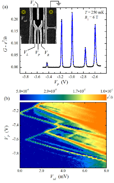
A scanning electron micrograph of the sample is shown in the inset of Fig. 1(a). Sample fabrication starts with patterning a 600 nm wide HSQ strip on the substrate by electron beam lithography (EBL)Lauvernier et al. (2004); Maex et al. (2003): film thickness is 60 nm. The central mesa region, aligned with the dielectric strip, is then defined by EBL and wet etching in a H3POH2O2 aqueous solution using a PMMA mask. Etching depth is 90 nm, ensuring removal also of the underlying -doping layer. Top metal gates are later patterned by EBL and liftoff on the dielectric. Finally ohmic side-contacts to the 2DEG are deposited by DC magnetron sputtering and liftoff. Low contact resistance was achieved by in situ argon plasma cleaning thanks to the negligible Schottky barrier. The measured resistance of the 2.5 m-wide mesa strip is 160 .
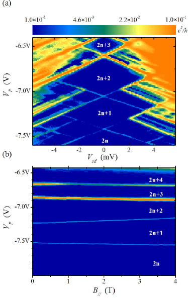
Electrical measurements are performed in a filtered 3He cryostat with 250 mK base temperature by lock-in technique. A DC voltage plus a V AC excitation are applied to the source electrode, with the drain electrode connected to the system ground through the input resistance of a low-noise current amplifier. Figures 1(a) and (b) show representative low-temperature transport characteristics, typical of a QD in the Coulomb blockade regimeKouwenhoven et al. (2001): as and are swept, diamond-shaped regions of reduced conductance are found [Figs. 1(b) and 2(a)]. Within each diamond conductance is strongly suppressed by Coulomb repulsion, and the island is populated by a constant number of electrons. At the edges of these diamonds the electrochemical potential in one of the leads is aligned to a QD resonance, thus lifting the blockade. The half width of the nth diamond is a direct measurement of the addition energy . Although we are not able to completely deplete the dot, the significant fluctuations in , together with the large energy spacings and are typical of a dot in the few-electron regimeKouwenhoven et al. (2001).
The ratio of to zero-bias peak separations allows us to estimate an average lever arm , that variesNot by in the range of plunger voltages shown in Fig. 2. Additional lines that run parallel to diamond edges appear when is sufficiently large to allow conduction through excited QD states. Data in Figs. 1(b) and 2(a) allow us to estimate single-particle energy spacing exceeding 1 meV.
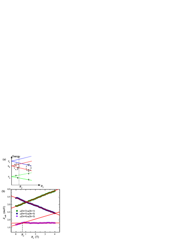
The spin filling sequence of a QD can be inferred from the chemical-potential evolution under parallel magnetic field . Figure 2(b) shows the measured zero-bias peaks in a plane, while the extracted are reported in Fig. 3(b). Data are consistent with the energy diagram depicted in Fig. 3(a): single-particle orbital states , with energies and are non degenerate and all empty when electrons are in the dot. At magnetic fields T we observe the usual antiferromagnetic filling, i.e. electrons are added with alternating spin orientation: , , , . Addition energies, in this case, are given by
| (1) | |||
| (2) | |||
| (3) |
where is the charging energy, are the level-dependent effective -factors, and is the Bohr magneton. The last two added electrons occupy the level with opposite spins and form a singlet.
As the magnetic field increases, the Zeeman energy brings levels and closer. As previously seen in similar QDsTarucha et al. (1996); Larsson et al. (2009), the exchange energy can be of the order of a fraction of meV and favors parallel spin filling. When , and transition to a triplet state takes place. In this configuration Eq. 3 must be replaced by
| (4) |
where is the effective -factor of level . For occupation numbers and the addition energy equals the charging energy . The observed marked dependence of the latter on is a consequence of our dot design and of the high 2DEG density. By fitting (1) and (2) to the data in Fig. 3(b), we obtain the effective factor moduli and . For T the addition energy is constant, therefore .
In conclusion, we have shown that it possible to reproducibly obtain metal-gate insulation and stable QDs on In.75Ga.25As/In.75Al.25As heterostructures using EBL-patterned HSQ. Thanks to the large value of the gyromagnetic factor coincidence between singlet and triplet states was observed at low magnetic field values. This technique can open the way to the application of In.75Ga.25As lateral QDs for spin manipulation and quantum computing architectures.
We acknowledge S. De Franceschi for helpful discussions and the E.U. project HYSWITCH (grant No. FP6-517567) for financial support. F.G. acknowledges the NanoSciERA “NanoFridge” project for partial financial support.
References
- Loss and DiVincenzo (1998) D. Loss and D. P. DiVincenzo, Phys. Rev. A 57, 120 (1998).
- Hanson et al. (2007) R. Hanson, L. P. Kouwenhoven, J. R. Petta, S. Tarucha, and L. M. K. Vandersypen, Rev. Mod. Phys. 79, 1217 (2007).
- Petta et al. (2005) J. R. Petta, A. C. Johnson, J. M. Taylor, E. A. Laird, A. Yacoby, M. D. Lukin, C. M. Marcus, M. P. Hanson, and A. C. Gossard, Science 309, 2180 (2005).
- Pioro-Ladriere et al. (2008) M. Pioro-Ladriere, T. Obata, Y. Tokura, Y.-S. Shin, T. Kubo, K. Yoshida, T. Taniyama, and S. Tarucha, Nat. Phys. 4, 776 (2008).
- Nowack et al. (2007) K. C. Nowack, F. H. L. Koppens, Y. V. Nazarov, and L. M. K. Vandersypen, Science 318, 1430 (2007).
- Kowalski et al. (1994) B. Kowalski, P. Omling, B. K. Meyer, D. M. Hofmann, C. Wetzel, V. Härle, F. Scholz, and P. Sobkowicz, Phys. Rev. B 49, 14786 (1994).
- Nitta et al. (1997) J. Nitta, T. Akazaki, H. Takayanagi, and T. Enoki, Phys. Rev. Lett. 78, 1335 (1997).
- Desrat et al. (2004) W. Desrat, F. Giazotto, V. Pellegrini, F. Beltram, F. Capotondi, G. Biasiol, L. Sorba, and D. K. Maude, Phys. Rev. B 69, 245324 (2004).
- Taddei et al. (2005) F. Taddei, F. Giazotto, and R. Fazio, J. Comput. Theor. Nanosci. 2, 329 (2005).
- Carillo et al. (2008) F. Carillo, D. Born, V. Pellegrini, F. Tafuri, G. Biasiol, L. Sorba, and F. Beltram, Phys. Rev. B 78, 052506 (2008).
- Schäpers et al. (1997) T. Schäpers, A. Kaluza, K. Neurohr, J. Malindretos, G. Crecelius, A. van der Hart, H. Hardtdegen, and H. Luth, Appl. Phys. Lett. 71, 3575 (1997).
- Csonka et al. (2008) S. Csonka, L. Hofstetter, F. Freitag, S. Oberholzer, C. Schönenberger, T. S. Jespersen, M. Aagesen, and J. Nygard, Nano Lett. 8, 3932 (2008).
- Björk et al. (2005) M. T. Björk, A. Fuhrer, A. E. Hansen, M. W. Larsson, L. E. Fröberg, and L. Samuelson, Phys. Rev. B 72, 201307 (2005).
- Sun et al. (2009) J. Sun, M. Larsson, I. Maximov, H. Hardtdegen, and H. Q. Xu, Appl. Phys. Lett. 94, 042114 (2009).
- Larsson et al. (2008) M. Larsson, D. Wallin, and H. Q. Xu, J. Appl. Phys. 103, 086101 (2008).
- Larsson et al. (2009) M. Larsson, H. A. Nilsson, H. Hardtdegen, and H. Q. Xu, Appl. Phys. Lett. 95, 192112 (2009).
- Schäpers et al. (2007) T. Schäpers, V. A. Guzenko, and H. Hardtdegen, Appl. Phys. Lett. 90, 122107 (2007).
- Capotondi et al. (2004) F. Capotondi, G. Biasiol, I. Vobornik, L. Sorba, F. Giazotto, A. Cavallini, and B. Fraboni, J. Vac. Sci. Technol. B 22, 702 (2004).
- Capotondi et al. (2005) F. Capotondi, G. Biasiol, D. Ercolani, V. Grillo, E. Carlino, F. Romanato, and L. Sorba, Thin Solid Films 484, 400 (2005).
- Lauvernier et al. (2004) D. Lauvernier, J.-P. Vilcot, M. Fran ois, and D. Decoster, Microelectr. Eng. 75, 177 (2004).
- Maex et al. (2003) K. Maex, M. R. Baklanov, D. Shamiryan, F. lacopi, S. H. Brongersma, and Z. S. Yanovitskaya, J. Appl. Phys. 93, 8793 (2003).
- Beenakker (1991) C. W. J. Beenakker, Phys. Rev. B 44, 1646 (1991).
- Kouwenhoven et al. (2001) L. P. Kouwenhoven, D. G. Austing, and S. Tarucha, Rep. Progr. Phys. 64, 701 (2001).
- (24) In order to account for this variation when converting plunger voltage values into an energy scale, we interpolated the lever arm with a order polynomial.
- Tarucha et al. (1996) S. Tarucha, D. G. Austing, T. Honda, R. J. van der Hage, and L. P. Kouwenhoven, Phys. Rev. Lett. 77, 3613 (1996).