The influence of Ga+-irradiation on the transport properties of mesoscopic conducting thin films
Abstract
We studied the influence of 30 keV Ga+-ions – commonly used in focused ion beam (FIB) devices – on the transport properties of thin crystalline graphite flake, La0.7Ca0.3MnO3 and Co thin films. The changes of the electrical resistance were measured in-situ during irradiation and also the temperature and magnetic field dependence before and after irradiation. Our results show that the transport properties of these materials strongly change at Ga+ fluences much below those used for patterning and ion beam induced deposition (IBID), limiting seriously the use of FIB when the intrinsic properties of the materials of interest are of importance. We present a method that can be used to protect the sample as well as to produce selectively irradiation-induced changes.
pacs:
81.05.Uw,73.21.-b,72.20.My1 Introduction
In the last years a focused ion beam (FIB) of Ga+-ions for etching [1] has attracted the attention of the community as an alternative and flexible method to produce micro- and nanostructures of materials, especially where the use of conventional methods appears to be limited. This FIB technique has been successfully used for nanostructuring different materials like magnetic and superconducting [2, 3, 4] or more recently to study the conduction behavior in metallic constrictions [5]. One of the advantages of this technique is its versatility; the use of any resist appears, a priory, unnecessary. Nowadays, FIB devices are also used for deposition of metallic or insulating materials with the help of the same Ga+-ions. These ions induce a decomposition of a chemical metal precursor over the surface in question, a technique called ion-beam induced or assisted deposition (IBID,IBAD) [6, 7, 8]. The main advantage of IBID/EBID is the deposition of the desired patterns of a material without the need of a mask or a pre-structured pattern using optical or e-beam lithography (EBL). Also the possibility to modify only parts of the patterns in electronic devices within nanometer dimensions is other of the FIB advantages.
The modification of different properties of different materials has been studied in the past, as e.g. in magnetic La0.7Sr0.3MnO3 thin films [9] or Co/Pt multilayers [10]. However, a fundamental problem of FIB was less discussed in literature, namely the modification of the sample near surface region and to a certain extent also its interior and their influence in the transport properties by the use of Ga+ions of energies up to 30 keV and fluences below cm-2 in usual devices. We note that before cutting or depositing material, the use of FIB requires the precise alignment of the Ga-beam and this is done taking a picture of the region in question irradiating it with the same Ga+-ions. Depending on the surface properties of the material in question, in general Ga+ fluences cm-2 are used. As we demonstrate below, these Ga+-fluences necessary for the first alignment may already affect seriously the intrinsic properties of the material of interest and can lead to wrong interpretations of the effects that a reduction of the sample geometry may produce.
The influence of Ga irradiation during the FIB preparation processes was not yet quantitatively studied, neither in situ nor after irradiation for fluences below cm-2. Specially when materials are selected to investigate their transport properties while their size is being reduced, care should be taken since the electrical transport can be sensitive to lattice defects as well as to the produced Ga contamination. The aim of this paper is to report on the changes in the electrical resistivity measured in-situ and its temperature and magnetic field dependence after irradiation of three different thin film materials to show the influence of the Ga irradiation used in FIB devices and at fluences as low as the ones used for beam alignment. The experiments were realized in two stages. In the first stage we have done in-situ measurements of the electrical resistance during irradiation and in the second stage its resistance was measured as a function of and to compare with the corresponding virgin states. Using graphite as a test material because its electrical resistance is extremely sensitive to lattice defects [11], we provide in this work a possible solution that can be used to strongly diminish the effects due to the Ga+-irradiation on different materials.
2 Experimental Details
| Sample | graphite | La0.7Ca0.3MnO3 | Co#2 |
|---|---|---|---|
| Dimensions (m) | |||
| Fluence (cm-2) | 5 (10) |
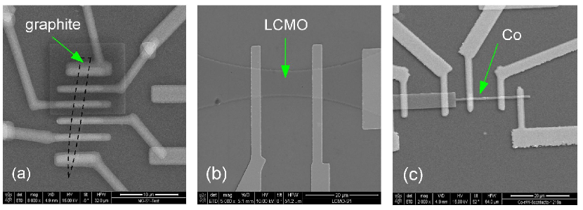
We have used the FIB capabilities of a FEI NanoLab XT 200 Dual Beam microscope (DBM). The acceleration voltage was fixed in all our experiments to 30 kV. The ion current and the area to be irradiated were changed in order to obtain different Ga+-fluences, see Table 1. The selected samples were a crystalline graphite flake prepared by a rubbing and ultrasonic process and pre-characterized with electron backscattering diffraction (EBSD) and Raman scattering [12, 11], a La0.7Ca0.3MnO3 (LCMO) thin film prepared by plasma laser deposition (PLD) and micro-structured by EBL and wet etching process [13], and thermal evaporated Co thin films (#1 and #2) previously structured by EBL, see Fig. 1(a-c) and Table 1.
Low-noise four-wires resistance measurements (two for the input current and two for the voltage measurement, important to eliminates contributions of the lead resistance) have been performed with the AC technique (Linear Research LR-700 Bridge with 8 channels LR-720 multiplexer) with ppm resolution and in some cases also with the DC technique (Keithley 2182 with 2001 Nanovoltmeter and Keithley 6221 current source).
The Au/Pt lead contacts used for all samples were prepared by EBL process using a e-beam resist PMMA 950K of nm thickness. The lithography process was done with the Raith ELPHY Plus system included in our microscope. The Au/Pt deposition of the contact electrodes was done by evaporation in a high-vacuum chamber with a nominal thickness of 25 and 9 nm, respectively. The in-situ resistance measurements performed before and during the irradiation of the sample were done using a self-made sample holder fixed inside the microscope chamber. The temperature and magnetic field dependence measurements were performed using a commercial cryostat with a temperature stability of 0.1 mK at 100 K. The magnetic field generated by a superconducting solenoid was always applied normal to the sample and input current.
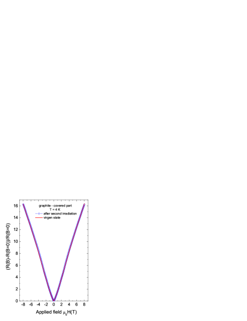
To avoid or diminish irradiation effects we protected the graphite sample with a negative electron beam resist (AR-N 7500) of thickness of 300 nm. In order to test the effectiveness of the resist film to avoid contamination during irradiation, part of the graphite flake was covered with the above mentioned resist in an additional process after the Au/Pt leads were deposited on the sample, see Fig. 1(a). This resin protects the graphite sample in the region of the three upper electrodes, allowing us to compare the change in voltage in the unprotected, protected and intermediate regions.
The advantages of this resist is that it allows us the patterning by EBL in the desired shape, it is sufficiently robust in the used temperature range and it is a very bad electrical conductor. The penetration depth of the Ga+-ions in this resist as well as in the samples and the distribution of the density of vacancies as a function of sample depth were estimated taking into account their density and using Monte Carlo simulations given by the stopping and range of ions in matter (SRIM) [14, 15] taking into account the energy of the Ga+-ions, see Fig. 3.
3 Results and discussion
3.1 In-situ transport measurements
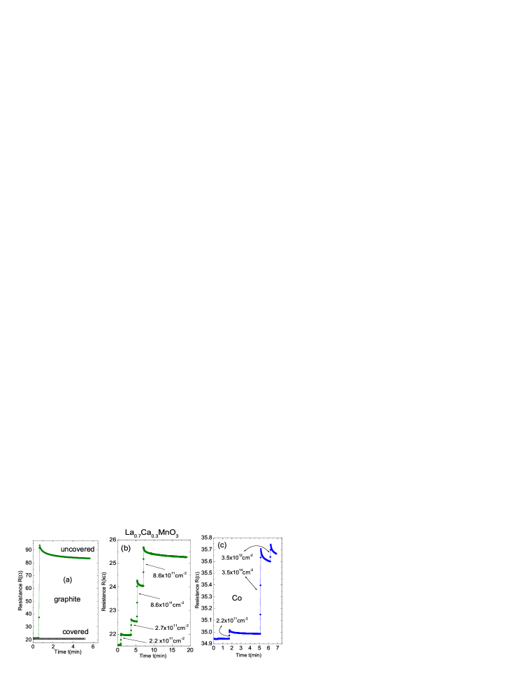
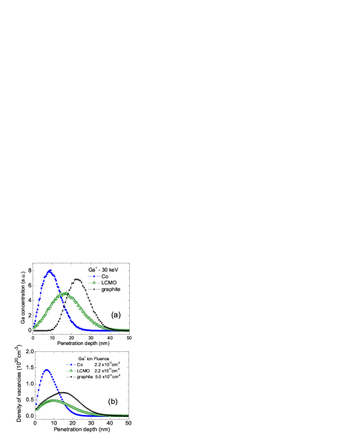
A detailed study of the electrical resistance of the above mentioned materials was realized in-situ during the Ga+-ion irradiation in the microscope chamber. In the case of the graphite sample we measured simultaneously the resistance of the covered and uncovered parts before, during and after irradiation. Figure 2 shows the changes observed in this sample during and after the first irradiation of fluence cm-2. This fluence produces nominally ppm vacancy concentration inside the sample whereas the Ga concentration implanted is less than 1 ppm, see Fig. 3. The disorder produced by the irradiation increases the resistance of the uncovered part of this sample by a factor .
The resistance of the covered part remains unchanged within relative change indicating that the 300 nm thick resist was enough to stop the Ga+-ions as expected since according the SRIM calculations the maximal penetration of the Ga+-ions in the resist should be nm. Immediately after irradiation the resistance of the uncovered part starts to decay exponentially with two characteristic relaxation times, as has been also observed after proton irradiation at room temperature [11]. This time relaxation is observed for all samples just after the irradiation finishes. This decay is related to local thermal relaxation process and to the diffusion of carbon interstitials and vacancies [16, 17].
Qualitatively speaking, similar resistance changes during the irradiation process are also observed in the two other samples, see Fig. 2(b,c). In the case of the LCMO sample the maximal penetration of the ions is nm, see Fig. 3(a). Because the thickness of this sample is 35 nm, part of the Ga+-ions are expected to be implanted and the rest to go through the sample generating a considerable amount of defects as can be seen in the calculated curves, see Fig. 3(b). In the case of the Co wire #1 the maximal ion penetration is nm nm thickness, see Fig. 3, therefore the produced defects plus Ga implantation are responsible for the relatively small increase in the electrical resistance, see Fig. 2(c). To study the influence on the transport properties mainly due to the produced defects by the Ga+ irradiation, a second Co #2 sample with less thickness has been studied and its results are discussed below.
The effect of the Ga irradiation to sample volume expansion (thickness swelling) as well as milling (thickness reduction) depends on the ion fluence, ion energy and target material. As an example we refer to the work done in Ref. [9] where such studies were done on La0.7Sr0.3MnO3 thin films. According to this work and taking into account our used fluences, any thickness increase as well as any milling are completely negligible and do not affect the changes measured in the resistance.
3.2 Temperature and magnetic field dependence before and after irradiation
1.Graphite: The special lattice structure of graphite and the weak coupling between graphene layers make graphite a quasi-2D semimetal, which carrier density depends strongly on the lattice defects like vacancies and/or impurities. In a recent work it was demonstrated that the electrical resistance of thin graphite crystals of micrometer size changes after inducing less than 1 ppm vacancy concentration by ion irradiation [11]. This makes graphite a extraordinary sensor for testing the efficiency of the resin cover as well as to show the dramatic changes produced by a relatively weak Ga+-ion irradiation fluence.
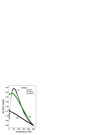
Figure 4 shows the temperature dependence of the graphite sample in its three states, as prepared and after the two irradiations. The temperature dependence in the as-prepared state has a semiconducting behavior above 50 K and metallic below. The semiconducting behavior is mainly due to the increase in carrier concentration with temperature because most of the carriers are thermally activated and the Fermi energy increases linearly with temperature [11]. The metallic behavior below 50 K is not intrinsic of graphite but comes from internal interfaces between crystalline regions parallel to the graphene layers but of slightly different orientation[12]. The mentioned interfaces originate during the pyrolysis process [18].
The first irradiation increased the resistance in all the temperature range without changing strongly the relative change with temperature, see Fig. 4. The metallic part was shifted to below 25 K and its -dependence gets weaker, suggesting that the irradiation also affected the properties of the internal interface(s). After the second irradiation the metallic region vanishes completely and the resistance decreases rather linearly with , see Fig. 4. We note that the absolute value of the resistance is fairly proportional to the used fluence. Between the virgin state and first irradiation we have an increase in the resistance of a factor of 3.5. Doubling the fluence we expect an increase of a factor of the resistance of the as-received state, a factor in agreement with the experimental observation.
As shown in [11] the increase in resistance is due to the decrease in the mean free path that overwhelms the increase in the carrier density that these irradiations produce inside the graphite structure. This behavior is related to difference weights the carrier density and the mean free path have in the 2D resistivity, i.e. in contrast with the 3D resistivity equation . Note also that the second irradiation produces already a vacancy density that implies a vacancy distance of less than 2 nm in the graphene plane. At distances smaller than nm we do not expect a large increase in the carrier density with further irradiation [11].
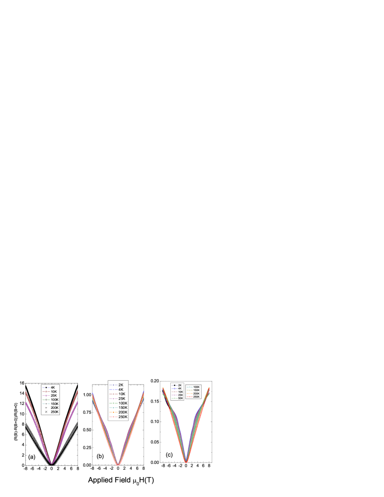
Figure 5 shows the magnetoresistance (MR) vs. applied field at different constant temperatures for the graphite sample in the virgin (a), first (b) and second (c) irradiated state. The MR in the virgin state agrees with previous reports [12]. Note that the MR shows a quasi linear field behavior at low temperatures. Also anomalous is the systematic increase of the MR below 100 K. This is related to the decrease in the resistance with decreasing temperature, see Fig. 4. The MR reaches a value of 16 at 8 T and 2 K. After the first irradiation the MR decreased a factor 16 and remains practically temperature independent. After the second irradiation the MR decreased further a factor of 6 and shows a similar temperature independence. The data reveal that the Shubnikov-de Haas (SdH) oscillations increase their amplitude and start to be measurable at lower fields after the first irradiation [11]. This behavior is related to the increase in the carrier density due to the creation of defects, whereas the decrease in the MR is due to the decrease in the mean free path.

Note that after the second irradiation the SdH oscillations do not change qualitatively (their absolute amplitude changes due to the large change of the MR), see Fig. 6. After the second irradiation we observe the first low-field oscillation at a similar field and a similar oscillation period in reciprocal field as after the first irradiation, see Fig. 6. These results indicate that no further change in the carrier density has been produced for a vacancy distance less than 2 nm. Taking into account that 3 nm is of the order of the range of modification of the electronic structure produced by, e.g. a single vacancy [19], then a saturation of the carrier density is reached decreasing the vacancy distance below nm but keeping the graphene structure. As expected, the covered part of the sample does not show any change after the first or second irradiation, as can be seen in Fig. 7.
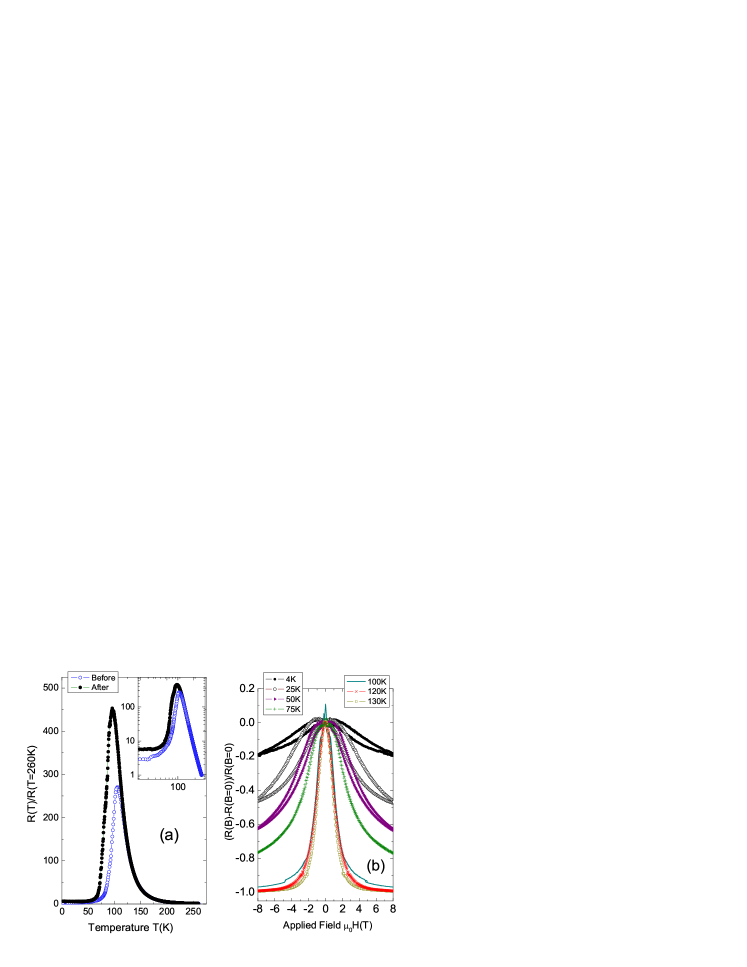
2.LaCaMnO film: The manganite sample undergoes a paramagnetic insulator to ferromagnetic metal transition leading to a sharp peak in the resistance near its Curie temperature as shown in Fig. 8(a). For our sample this peak is observed at K. Interestingly, after irradiation the temperature dependence does change only in the ferromagnetic state of the sample, which shows now a K, see Fig. 8(a). The measured MR of this sample in the as-prepared state agrees with published literature and shows hysteretic behavior in the ferromagnetic state whereas no hysteresis in the paramagnetic state above , see Fig. 8(b).
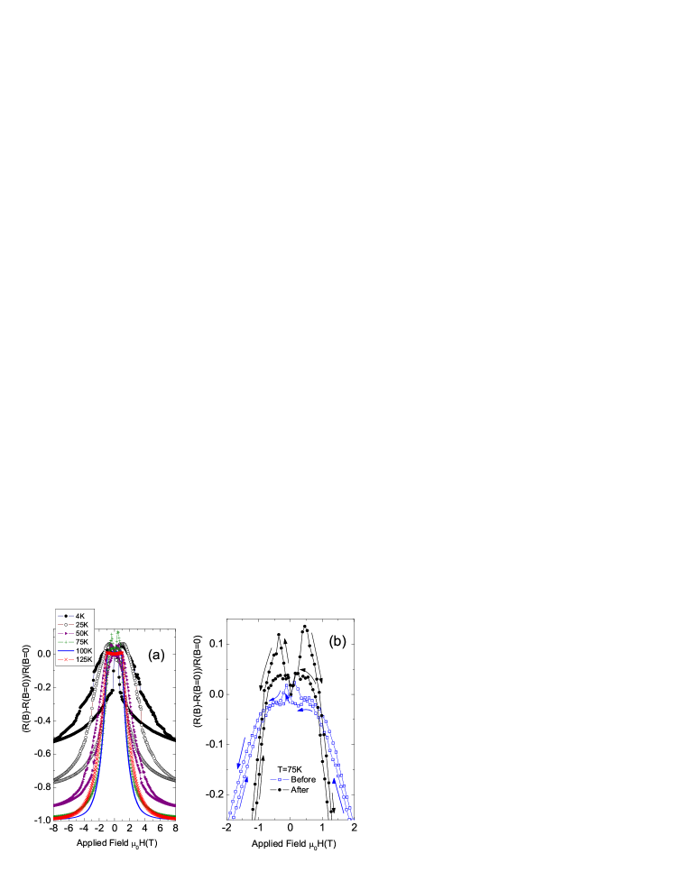
The influence of ion irradiation on the magnetic and transport properties of manganites were studied in the past but mainly at much higher ion-energies, see e.g. Refs. [20, 21, 22, 23, 9]. In general at fluences above cm-2 the ion irradiation decreases the metal-insulator transition temperature and the magnetic hysteresis gets broader reflecting the increase of the pinning of the domain walls by the induced defects. A similar behavior is observed in our sample, see Fig. 9(a). Figure 9(b) shows in detail the MR between -2 T and 2 T at 75 K. The irradiation induces an increase in the coercivity , from 0.1 T to 0.42 T after irradiation, defined at the maxima of the MR, as well as in the overall hysteresis width.
These results indicate that care should be taken when changes in the transport properties of ferromagnetic oxides are observed after microstructuring the samples with FIB. The observed results after patterning might not be due to the change of the sample dimension but to the induced structural changes by the Ga+ irradiation.
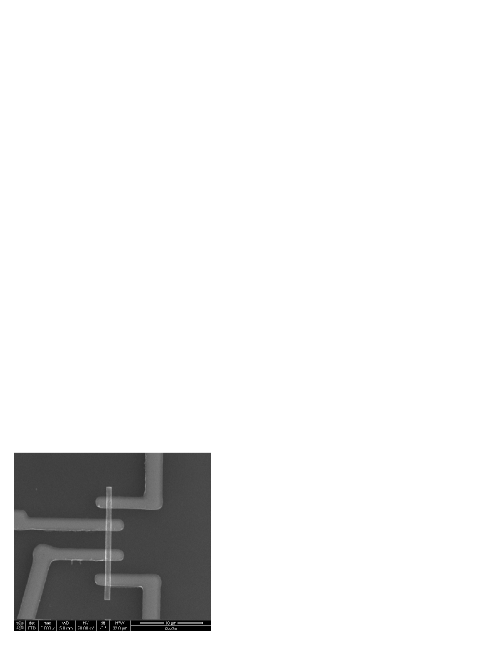
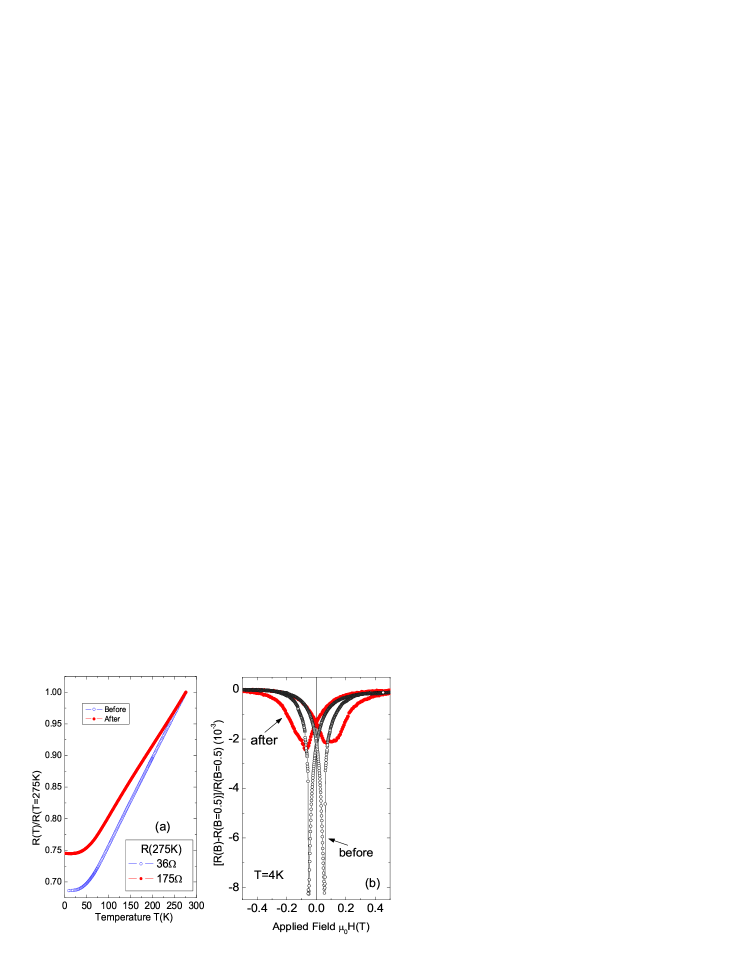
3.Co film: Figure 10 shows a SEM picture of the Co-sample #2 with the four electrodes for the resistance measurement. The resistance as a function of temperature and magnetic field before and after a Ga+ irradiation is shown in Fig. 11(a) and (b). Due to the smaller thickness of this sample the irradiation at 30 kV produces mainly defects instead of doping since the Ga+ ions stop beyond the sample thickness, i.e. inside the substrate. The influence of the induced defects in the Co sample can be clearly recognized by the increase in the absolute value of the resistance. For example at 275 K the resistance of the Co-sample #2 increases from to flattening the temperature dependence, see Fig. 11(a). The MR shown in Fig. 11(b) indicates a clear change in the hysteresis indicating a change in pinning of the domain walls. These results are qualitatively similar to those obtained for the manganite shown above, see Fig. 9.
4 Conclusion
In conclusion our studies indicate clearly that care should be taken with the change of the intrinsic properties of the materials when FIB devices are used for patterning, cutting or just for deposit other materials for contacts, for example. Our work demonstrates that already the usual Ga+ fluences needed for a precise alignment of the Ga+ beam before really using it, induce relevant changes in the transport properties of the three different materials studied here. Using a thin crystalline graphite flake we were able to demonstrate also that covering the sample with a sufficiently thick resist film one can avoid the irradiation damage completely. This indicates that in principle one can use this technique to protect certain parts and produce defined changes in other parts of the sample of interest. This method might be used to induce changes in the hysteretic properties of ferromagnetic micro and nano-structures or in the electronic density in graphite or multigraphene in specific parts of the sample, for example.
References
- [1] S. Matsui, Kojima. Y., Y. Ichiai, and T. Honda. J. Vac. Sci. Technol. B, 9:2622–2632, 1991.
- [2] J. Gierak. Microelectronic Engineering, 78–79:266–278, 2005.
- [3] A. A. Tseng. Small, 10:924–939, 2005.
- [4] M. de la Pierre, S. Cagliero, A. Agostino, G. Gazzadi, and M. Truccato. Supercond. Sci. Technol., 22:045011, 2009.
- [5] A. Fernández-Pacheco, J. M. De Teresa, R Córdoba, and M. R. Ibarra. Nanotechnology, 19:415302, 2008.
- [6] J. Melngailis. J. Vac. Sci. Technol. B, 5:469, 1987.
- [7] S. Matsui and Y. Ochiai. Nanotechnology, 7:247, 1996.
- [8] R. M. Langford, A. K. Petford-Long, M. Rommeswinkle, and S. Eagelkamp. Mater. Sci. Technol., 18:743, 2002.
- [9] I. Pallecchi, L. Pellegrino, E. Bellingeri, A.S. Siri, D. Marré, and G.C. Gazzadi. J. Magn. Magn. Mater., 320:1945–1951, 2008.
- [10] R. Hyndman, P. Warin, J. Gierak, J. Ferre, J. N. Chapman, J. P. Jamet, V. Mathet, and C. Chappert. Journal of Applied Physics, 90:3843–3849, 2001.
- [11] A. Arndt, D. Spoddig, P. Esquinazi, J. Barzola-Quiquia, S. Dusari, and T. Butz. Phys. Rev. B, 80:195402, 2009.
- [12] J. Barzola-Quiquia, J.-L. Yao, P. Rödiger, K. Schindler, and P. Esquinazi. phys. stat. sol. (a), 205:2924–2933, 2008.
- [13] G. Bridoux and J. Barzola-Quiquia and F. Bern and W. Böhlmann and P. Esquinazi and M. Ziese, (unpublished) patent pending.
- [14] J. F. Ziegler. The stopping and range of ions in matter. Pergamon Press, New York, 1977-1985.
- [15] J. F. Ziegler, J. P. Biersack, and M. D. Ziegler. SRIM - The Stopping and Range of Ions in Matter. SRIM Co., 2008. ISBN 0-9654207-1-X. See also the simulation software IIS available at http://www.ele.uva.es/ jesman/iis.html, which has some advantages in comparison with the usual SRIM simulation.
- [16] K Niwase. Irradiation-induced amorphization of graphite. Phys. Rev. B, 52:15785–15798, 1995.
- [17] G.-D. Lee, C. Z. Wang, E. Yoon, N.-M. Hwang, D.-Y. Kim, and K. M. Ho. Phys. Rev. Lett., 95:205501, 2005.
- [18] As an example, one can take the process or graphitization of Kapton [24, 25]. Kapton is a polyimide, commercially available as thin films of different thickness. This polyimide has the advantage that through its carbonization at high temperatures and high pressures, it transforms into highly ordered graphite with properties similar to highly oriented pyrolytic graphite (HOPG) [25]. In general, during the graphitization the crystalline regions grow through different steps at different temperatures and pressures where the release of different gases, like CO, CO2, CH4, H2, N2, occurs [25]. Through the fabrication process these graphite single crystals within the carbon matrix do not grow with a thickness larger than nm [12], whereas the high degree of orientation remains in the ten micrometer size along the or directions, i.e. parallel to the graphene planes [25, 26, 12]. It appears plausible that structural defective regions, generated during the grow process and influenced by the release of gases, prevent a larger growth of the thickness of the crystalline regions, producing these planar interfaces.
- [19] R. Ruffieux, O. Gröning, P. Schwaller, L. Schlapbach, and P. Gröning. Phys. Rev. Lett., 84:4910–4914, 2000.
- [20] R. M. Stroud, V. M. Browing, J. M. Byers, D. B. Chrisey, W. W. Fuller-Mora, K. S. Grabowski, J. S. Horwitz, J. Kim, D. L. Knies, and M. S. Osofsky. MRS, Symposium V:154, 1997.
- [21] J. Wolfman, M. Hervieu, and Ch. Simon. Nuclear Instruments and Methods in Physics Research B, 179:176–185, 2001.
- [22] S. Chattopadhyay, S. Pal, A. Sarkar, R. Kumar, and B. K. Chaudhuri. Nuclear Instruments and Methods in Physics Research B, 230:274–278, 2005.
- [23] M. Ramesh Babu, X. F. Han, P. Mandal, R. Kumar, K. Asokan, and R. Jayavel. Materials Chemistry and Physics, 117:113–116, 2009.
- [24] Y. Hishiyama, S. Yasuda, A. Yoshida, and M. Inagaki. J. Mater. Sci., 23:3272, 1988.
- [25] M. Inagaki. New Carbons: Control of Structure and Functions. Elsevier, 2000.
- [26] N. García, P. Esquinazi, J. Barzola-Quiquia, B. Ming, and D. Spoddig. Phys. Rev. B, 78:035413, 2008.