Fabrication and characterization of an induced GaAs single hole transistor
Abstract
We have fabricated and characterized a single hole transistor in an undoped AlGaAs-GaAs heterostructure. Our device consists of a p-type quantum dot, populated using an electric field rather than modulation doping. Low temperature transport measurements reveal periodic conductance oscillations due to Coulomb blockade. We find that the low frequency charge noise is comparable to that in modulation-doped GaAs single electron transistors (SETs), and an order of magnitude better than in silicon SETs.
The ability to isolate and control single spins in solid state systems is a problem of significant interest. Although systems such as P nuclei in Si KaneNature98 and Nitrogen-vacancy centers in diamond WrachtrupJPCM06 have emerged, electron quantum dots defined using surface-gate techniques on AlGaAs/GaAs heterostructures have, due to their purity and maturity, been the focus of most attention. ElzermanNature04 ; KoppensNature06 ; KouwenhovenPSS06 ; HansonRMP07 However, a major limitation of electron quantum dots is randomization of the electron’s spin orientation due to hyperfine interactions with Ga and As nuclei. There are two material-based ways to overcome this problem. One is to use materials with spin zero nuclei such as 12C or 28Si. The alternative is to retain the advantages of the AlGaAs/GaAs system by using holes rather than electrons. Holes experience a much weaker hyperfine coupling, resulting in a significantly enhanced spin coherence lifetime, BulaevPRL07 as demonstrated by optical measurements of self-assembled hole quantum dots. BrunnerScience09 However, reports on the electronic properties of hole quantum dots are scarce, GrbicAPL05 ; KomijaniEPL08 due to the poor stability of surface-gate defined hole devices. EnsslinNatPhys06 ; Taskinen09
We have previously shown that it is possible to make stable hole quantum wires using an ‘induced’ approach where the device is populated electrostatically using a biased gate rather than by modulation doping. ClarkeJAP06 ; KlochanAPL06 In this letter, we extend this technique to realize a stable hole quantum dot, which we demonstrate by operating as single hole transistor. This type of device could in the future be used as a system for isolating, manipulating and studying single hole spins.
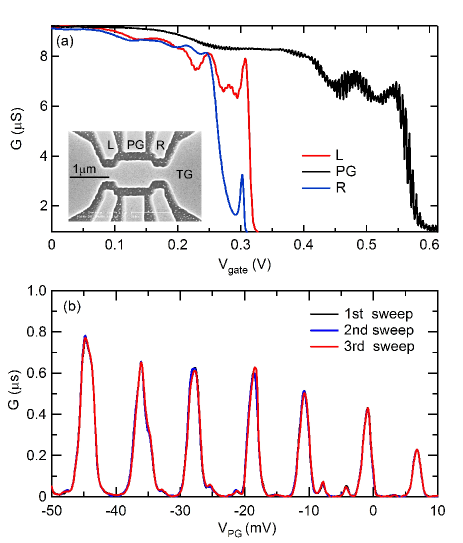
Our devices were fabricated on a (311)A-oriented AlGaAs/GaAs heterostructure featuring (from undoped GaAs buffer upwards): a nm undoped AlGaAs barrier, a nm GaAs spacer, and a nm p+-GaAs cap (degenerately doped with Si as an acceptor to cm-3) used as a metallic gate. Annealed AuBe Ohmic contacts, fabricated using a self-aligned process, KaneAPL93 provide electrical contact to the two-dimensional hole system (2DHS) that forms at the AlGaAs/GaAs interface. The p+-gate layer is divided into seven independent gates using electron-beam lithography and shallow wet etching, as shown Fig. 1(a) inset. The largest gate is the top gate, which leads to an accumulation of holes when negatively biased to V, populating the dot and the adjacent 2DHS reservoirs. The four gates in the corners define two quantum point contacts (denoted L and R) used to control the transparency of the leads connecting the quantum dot to the reservoirs. The two plunger gates (PG) are used to control the number of holes in the dot. The resulting dot has lithographic dimensions nm. Electrical studies were performed in a dilution refrigerator, with a minimum hole temperature of mK. The two-terminal conductance was measured using lock-in techniques with a V ac excitation at Hz. The series resistance was dominated by the Ohmic contacts, which had a resistance of k.

We begin in Fig. 1(a) by characterizing the quantum point contact (QPC) and plunger gates. The top-gate bias was set to V to give a hole density cm-2 in the 2D reservoirs and populate the dot. At this density, the mobility in the reservoirs was cmVs. Increasing the positive bias on the left or right QPCs generates a series of steps in the conductance as the 1D subbands in the dot’s entrance and exit leads are depopulated. The pinch-off voltages (i.e., where becomes zero) for the two QPCs are identical to within . Increasing also causes steps in conductance, and leads to Coulomb Blockade (CB) oscillations with a period of mV. These CB oscillations persist even with the QPC gates unbiased, in contrast to modulation-doped devices. The oscillations become more prominent at more positive bias because capacitive coupling between the plunger gate and the entrance and exit constrictions makes them less transparent.
To enhance the CB oscillations we increase to V ( cm-2) and then increase and until the entrance and exit leads are fully closed and no current passes through the dot. A small negative bias is then applied to the bottom plunger gate (top plunger gate remains unbiased), which has two effects: it opens the entrance and exit leads slightly, and tunes the hole density (i.e., occupancy) of the dot. In Fig. 1(b) we plot versus bottom plunger gate bias, and obtain well-defined CB peaks separated by regions of zero conductance. To demonstrate the stability of our device, we show sweeps of repeated for a second (blue) and third (red) time, which show no change in the peak locations in and almost negligible variations in peak amplitude. For mV (i.e., beyond the left axis in Fig. 1(a)) the peak amplitude increases rapidly and the conductance minima rise above , similar to the behavior at V in Fig. 1(a). We observe a variation in the period of oscillations from to mV, similar to that in Ref. GrbicAPL05 . In addition to the primary CB oscillations we also observe higher frequency oscillations with reduced amplitude. In order to confirm that the smaller higher frequency peaks are not resonances caused by background impurities, we applied a small perpendicular field T; the peaks were unaffected by this. It is also unlikely that these peaks arise because the dot has broken into two or more smaller dots, since the smaller dots would have a smaller capacitance to the gates and hence show lower frequency oscillations, contrary to what we observe. One possibility is that the two sets of CB oscillations are due to the interplay between the light-hole and heavy-hole energy levels in the entrance and exit QPCs: in our 2D hole system the ground state is heavy-hole-like, whereas in a tightly confined 1D system the ground state is light-hole-like. CsontosPRB07 This will be the focus of a more extended study in the future.

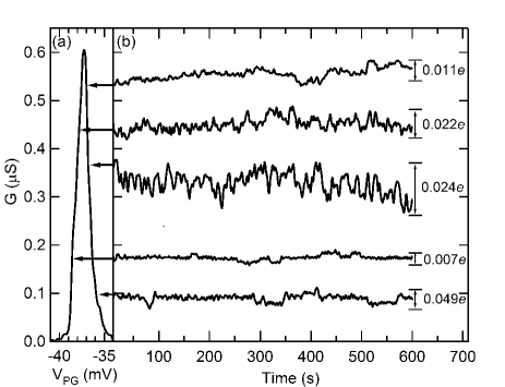
A common characteristic of modulation-doped hole quantum devices is poor temporal stability, with a tendency for the conductance to drift over long time scales even when the gate biases are all held constant. DaneshvarPRB97 This is particularly undesirable for quantum dot devices, which are often used as highly sensitive electrometers due to their high transconductance. FujisawaScience06 The conductance fluctuations are typically due to charge noise caused by ionized dopants, which we seek to minimize with the undoped device design presented here. To further gauge the effectiveness of our approach, in Fig. 2 we present stability tests performed by setting five different operating points (Fig. 2(a)) on the CB peak centered at mV in Fig. 1(b), and measuring over a ten minute period (see Fig. 2(b)). In each case, the average conductance remains approximately constant, despite some random fluctuations. These fluctuations are small, corresponding to a charge fluctuation between and of an electron over the ten minute period. We extract the power spectral density from an analysis of these fluctuations, obtaining values ranging from to at a frequency Hz. This is almost an order of magnitude lower than the at Hz measured in undoped Si SETs, HourdakisAPL08 and compares very favorably with the at Hz measured in modulation-doped GaAs radio-frequency SETs. FujisawaAPL01 Note that -noise becomes more pronounced at lower frequencies, such that if equal values are obtained in two separate devices and at different frequencies , then device is significantly quieter. This highlights the superior noise performance that can be obtained with our induced GaAs single-hole transistor technology.
It is interesting to note evidence of random telegraph signals in the bottom two traces in Fig. 2(b). In modulation-doped devices this has been attributed to ionization/deionization of dopants in the modulation-doping layer or current leakage from the surface gates. BuizertPRL08 These mechanisms should be greatly reduced in our device due to the absence of modulation doping and the deliberate use of small top-gate bias to minimize the gate leakage current (measured as pA at V). Surface-state traps in the vicinity of the nm deep trench that was etched to define the gates are one possible origin of this noise. However, these traps would be at least nm from the dot, and their contribution is thus likely to be small. An alternative is that background impurities may have ionized during the low-temperature illumination of the device to improve the Ohmic contact resistance. Further studies utilizing higher bandwidth measurement techniques, TaskinenRSI08 and surface passivation BessolovSemi98 may help in determining the origin of the remaining noise in our devices.

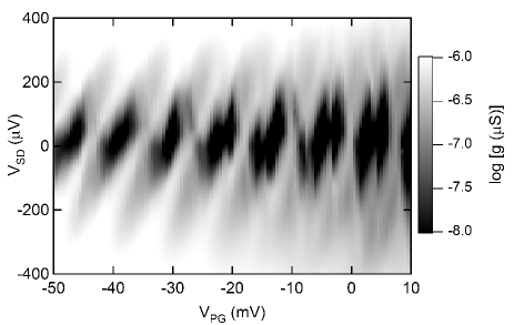
As a final characterization, we have used source-drain bias spectroscopy to determine the key energy scales for our dot. In Fig. 3 we present a grayscale plot of the differential conductance versus and applied dc source-drain bias , with Coulomb diamonds clearly evident. We note the presence of additional diamond-like features, which are related to the smaller high-frequency peaks in Fig. 1(b) rather than charge noise. We extract a charging energy ranging from to eV from an analysis of the Coulomb diamonds, corresponding to a total dot capacitance of aF. This is more than double that expected from the sum of the individual gate capacitances ( aF), suggesting significant capacitive coupling between the dot and the adjacent 2D reservoirs. From the dot’s lithographic dimensions and hole density, we estimate the dot occupancy to be less than holes, giving a single particle energy spacing eV. This is substantially smaller than eV, explaining why we do not observe excited state transport in our device (cf. Ref. KomijaniEPL08 ). Reducing the size of our dots to allow lower occupancy operation and the observation of excited-state transport, whilst maintaining their low noise characteristics, will be the focus of future work.
In summary, we have reported the fabrication of a GaAs single hole transistor using a heterostructure without modulation-doping. Our device shows stable electrical characteristics with little drift in conductance at fixed gate bias and significantly improved noise performance compared to both modulation-doped GaAs and undoped Si single electron transistors. The dot design we present here holds much promise for future studies of single hole spin manipulation.
This work was funded by the Australian Research Council (ARC). ARH was supported by an ARC Professorial Fellowship. We thank T. P. Martin and L. H. Ho for helpful discussions and J. Cochrane for technical support.
References
- (1) J. M. Elzerman, R. Hanson, L. H. Willems van Beveren, B. Witkamp, L. M. K. Vandersypen and L. P. Kouwenhoven, Nature 430, 431 (2004).
- (2) F. H. L. Koppens, C. Buizert, K. J. Tielrooij, I. T. Vink, K. C. Nowack, T. Meunier, L. P. Kouwenhoven and L. M. K. Vandersypen, Nature 442, 766 (2006).
- (3) L. P. Kouwenhoven, J. M. Elzerman, R. Hanson, L. H. Willems van Beveren, and L. M. K. Vandersypen, Phys. Stat. Solidi B 243, 3682 (2006).
- (4) R. Hanson, L. P. Kouwenhoven, J. R. Petta, S. Tarucha, and L. M. K. Vandersypen, Rev. Mod. Phys. 79, 1217 (2007).
- (5) B. E. Kane, Nature 393, 133 (1998).
- (6) J. Wrachtrup and F. Jelezko, J. Phys.: Condens Matter 18, S807 (2006).
- (7) D. V. Bulaev, and D. Loss, Phys. Rev. Lett. 98, 097202 (2007).
- (8) D. Brunner, B. D. Gerardot, P. A. Dalgarno, G. Wüst, K. Karrai, N. G. Stoltz, P. M. Petroff, and R. J. Warburton, Science 325, 70 (2009).
- (9) B. Grbić, R. Leturcq, K. Ensslin, D. Reuter, and A. D. Wieck, Appl. Phys. Lett. 87, 232108 (2005).
- (10) Y. Komijani, M. Csontos, T. Ihn, K. Ensslin, D. Reuter, and A. D. Wieck, Euro. Phys. Lett. 84, 57004 (2008).
- (11) K. Ensslin, Nature Physics 2, 587 (2006).
- (12) L. J. Taskinen et al, unpublished.
- (13) W. R. Clarke, A. P. Micolich, A. R. Hamilton, M. Y. Simmons, K. Muraki, and Y. Hirayama, J. Appl. Phys. 99, 023707 (2006).
- (14) O. Klochan, W. R. Clarke, R. Danneau, A. P. Micolich, L. H. Ho, A. R. Hamilton, K. Muraki, and Y. Hirayama, Appl. Phys. Lett. 89, 092105 (2006).
- (15) B. E. Kane, L. N. Pfeiffer, K. W. West, and C. K. Harnett, Appl. Phys. Lett. 63, 2132 (1993).
- (16) D. Csontos and U. Zülicke, Phys. Rev. B 76, 073313 (2007).
- (17) A. J. Daneshvar, C. J. B. Ford, A. R. Hamilton, M. Y. Simmons, M. Pepper, and D. A. Ritchie, Phys. Rev. B 55, R13409 (1997).
- (18) T. Fujisawa, T. Hayashi, R. Tomita and Y. Hirayama, Science 312, 1634 (2006).
- (19) E. Hourdakis, J. A. Wahl, and N. M. Zimmerman, Appl. Phys. Lett. 92, 062102 (2008).
- (20) T. Fujisawa and Y. Hirayama, Appl. Phys. Lett. 77, 543 (2000).
- (21) C. Buizert, F. H. L. Koppens, M. Pioro-Ladrière, P. Tranitz, I. T. Vink, S. Tarucha, W. Wegscheider and L. M. K. Vandersypen, Phys. Rev. Lett. 101, 226603 (2008).
- (22) L. J. Taskinen, R. P. Starrett, T. P. Martin, A. P. Micolich, A. R. Hamilton, M. Y. Simmons, D. A. Ritchie, and M. Pepper, Rev. Sci. Inst. 79, 123901 (2008).
- (23) V. N. Bessolov and M. V. Lebedev, Semiconductors 32, 1141 (1998).