Scanning Tunneling Microscopy studies on CeCoIn5 and CeIrIn5
Abstract
High–quality single crystals of the heavy fermion superconductors CeCoIn5 and CeIrIn5 have been studied by means of low–temperature Scanning Tunneling Microscopy. Methods were established to facilitate in-situ sample cleaving. Spectroscopy in CeCoIn5 reveals a gap which persists to above , possibly evidencing a precursor state to SC. Atomically resolved topographs show a rearrangement of the atoms at the crystal surface. This modification at the surface might influence the surface properties as detected by tunneling spectroscopy.
pacs:
71.27.+a, 74.70.Tx, 68.37.Ef, 06.60.EiI Introduction
During the past decade, the CeMIn (M = Co, Ir, Rh) family of heavy fermion (HF) compounds has attracted considerable scientific interest. The latter was largely motivated by the discovery of unconventional superconductivity (SC) in these materials hegger:00 ; petrovic:01a ; petrovic:01b ; sarrao:07 . Unlike in conventional superconductors, where tiny amounts of magnetic impurities suppress the superconducting state, HF superconductivity develops in an inherently magnetic environment. For instance, it was shown for the case of the prototypical HF superconductor CeCuSi that the complete occupancy of the corresponding lattice sites by the magnetic Ce3+ ions is necessary to generate SC steglich:79 . It is generally accepted that magnetic fluctuations may potentially induce electron pairing into a superconducting condensate schmitt-rink:86 ; scalapino:86 ; marthur:98 . The precise interplay between magnetism and SC in HF compounds, however, is not yet understood in all detail. The knowledge of the excitation spectrum of the superconducting quasiparticles is one crucial aspect for the understanding of the superconducting state.
In this paper we report the investigation of the HF superconductors CeCoIn and CeIrIn by means of Scanning Tunneling Microscopy (STM). An important and powerful feature of STM is the possibility to perform local spectroscopy on the atomic scale, referred to as Scanning Tunneling Spectroscopy (STS). By measuring the tunneling current at constant tip-sample distance as a function of the applied voltage, one can probe directly the electronic density of states (DOS) of the sample, and thereby obtain information on the charge degrees of freedom of the material investigated. The accessibility of SC at ambient pressure, as well as the – for HF compounds – comparably high transition temperatures (2.3 K and 0.4 K, respectively) render CeCoIn and CeIrIn ideal candidates to study HF superconductivity by STM. In both materials, the superconducting state is unconventional. The gap function has line nodes, and an order parameter with -wave symmetry has been suggested izawa:01 ; vorontsov:06 . Although the ground states are non-magnetic, strong antiferromagnetic fluctuations are present kohori:01 , and it has been speculated that these fluctuations mediate the superconducting pairing stock:08 ; kasahara:09 . Together with other experimental findings, the unconventional nature of SC and its close relationship to magnetism has lead to the suggestion that the 1:1:5 compounds are remarkably similar to the cuprate High- superconductors nagajima:07 .
We present STM/STS data obtained on single crystalline 1:1:5 samples. A gap compatible with -wave SC is observed in the conductance spectra of CeCoIn. The presence of a gap-like feature in a temperature range above might evidence a precursor state similar to the pseudogap phase in the underdoped cuprates. Based on atomically resolved topography data, the possible influence of a modified surface structure on STS is discussed.
II Experimental Details
The application of STM and, in particular, STS to HF superconductors has only become feasible very recently. One reason is that the involved energy scales are in the order of, or even less than 1 meV. This calls for both an excellent energy resolution and the accessibility of temperatures considerably lower than the superconducting transition temperatures . Our tunneling experiments were conducted in a 3He cryostat with a base temperature of 320 mK at the STM. In order to maintain an unperturbed vacuum tunnel junction over a sufficiently long period of time, the STM operates under UHV conditions ( mbar) omicron . An adequate energy resolution ( 80 V) of the STM has been verified by investigating the superconducting gap of Al. We used electrochemically etched tungsten tips which were conditioned in situ by Ne ion sputtering and electron beam annealing ernst:07 .
In order to obtain a clean tunnel junction in the first place, several methods for surface preparation have been applied to the single crystals. Samples treated by etching in HCl, by in situ radiative annealing, by Ar ion sputtering, or by a combination of these methods, exhibited extensive structural damage at the surface, including indium segregation. Therefore, such samples did not yield any reasonable STM results. However, both materials could successfully be cleaved in situ at room temperature. CeCoIn forms platelet–like crystals. The samples used in our experiments had a size of few hundred m along the c–axis, and up to 2 mm within the ab–plane. In order to facilitate the cleaving, a stainless steel post was glued onto a sample using strong epoxy epoxy . The post was then torn off in situ, often ripping off part of the sample and exposing a fresh surface. Since CeCoIn is rather ductile, it was found to be important to pull off the post straight in order to avoid shear forces while cleaving. The highest success rate was achieved when the post was polished at the face used for glueing. Furthermore, the shape of the post should be well adapted to the sample dimensions. In contrast, CeIrIn crystals are rather brittle and larger along the c–axis. These samples could be cleaved directly, using an in situ cleaving tool. The latter consists of two tungsten–carbide jaws that form a pair of pliers. Considering the layered crystal structure of the 1:1:5 materials, one might expect that the samples can easily be cleaved parallel to the ab–plane. However, the samples often did not cleave, but broke in an irregular fashion. In spite of the macroscopic roughness of the resulting surfaces it was still possible to perform tunneling experiments on microscopically small areas.
III Results
The primary objective of this work was to obtain spectroscopic information in the superconducting state of the 1:1:5 compounds. A gap was observed in the differential conductance spectra of CeCoIn. Figure 1 shows its temperature evolution between 320 mK and 3 K. The curves were acquired with a bias voltage of = 14 mV at a set-point current of 340 pA. was measured directly, using a lock–in amplifier with a modulation amplitude of 70 V at 180 Hz. For a better visibility the individual curves were shifted vertically. Upon increasing temperature the zero bias conductance increases, indicating a closing of the gap. The solid lines in the figure represent fits to the tunneling conductance, considering thermal broadening. For the superconducting order parameter, we assumed symmetry, which is likely to be present in CeCoIn izawa:01 ; vorontsov:06 . In this case, the BCS expression for the superconducting excitation spectrum takes the form won:94
| (1) |
where is the maximum value of the angular dependent gap function. The additional lifetime broadening parameter accounts for in-gap states due to inelastic scattering dynes:78 . A linear term has been included to the fit
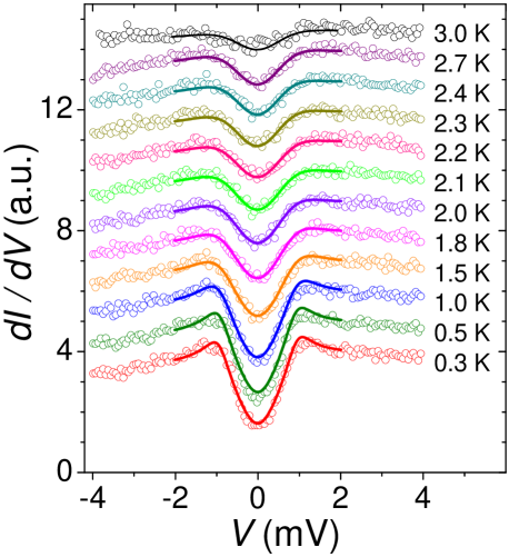
function in order to approximate the slightly asymmetric background. The fit parameters and are plotted vs. temperature in Fig. 2. The error bars are estimated from the fitting procedure. Expectedly, the superconducting order parameter decreases with temperature, whereas increases. The solid line represents a fit with an approximate expression for the temperature dependence of the order parameter in nodal superconductors dora:01 ,
| (2) |
Here, denotes the temperature at which extrapolates to zero.
The fit yields a zero-temperature value of the order parameter meV. Similar values were previously found in point contact spectroscopy experiments goll:03 ; rourke:05 , but also different values have been reported park:05 . The resulting ratio indicates that CeCoIn is a strong coupling superconductor. This is consistent with the large jump detected in the specific heat petrovic:01b . Notably, the gap does not close at K, but persists up to a temperature K. This behaviour is reminiscent of the pseudogap phase of underdoped cuprates renner:97 . Considering the striking similarities to the cuprates, it may be reasonable to expect similar effects in the 1:1:5’s. Indeed, a pseudogap above has been observed in electrical resistivity measurements on CeCoIn sidorov:02 . The value K extrapolated from our data is in agreement with the pseudogap temperature reported therein. Also for the other members
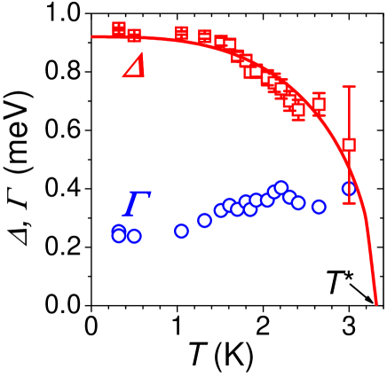
of the 1:1:5 family, the existence of a precursor state to SC has been reported nair:08 ; kawasaki:02 . At present, the nature of the precursor state is still speculative. In the case of CeIrIn, however, there is strong evidence that both SC and this state have a common origin. The data shown here support this idea, as the gap evolves continuously at around . As noted in Ref. izawa:01 , the fourfold anisotropy in the thermal conductivity persists to 3.2 K. Hence, a possible precursor state above might have the same -wave symmetry as the superconducting state.
Throughout our measurements, the gap in the tunneling conductance had a low spatial reproducibility, and many sample spots did not show any gap. Also in these cases, a clean vacuum tunnel junction was verified from the dependence of the tunneling current on the tip-sample distance yielding an effective work function eV. Hence, the variations over the surface area might have a different origin, such as changes in the composition or structure. Even on in-situ cleaved samples, the surface properties as detected by STM might locally differ significantly from those of the bulk fischer:07 . Topographic data obtained on CeIrIn hints toward this possibility. Figure 3 exemplifies an atomically-resolved topograph acquired on an in-situ cleaved sample. The image reveals different atomic sites: In addition to the most prominent corrugations (marked as “A” in the figure), other sites can be identified in between (marked as “B”). Different arrangements of the surface atoms are clearly visible within the image. The corrugations of type A form either a triangular lattice, or a rectangular one, as indicated by the respective markers. The two different arrangements merge through dislocations due to a defect. In order to identify the crystallographic plane visible in the figure, we compared the data with the lattice dimensions of CeIrIn. The sample had been mounted parallel to the ab-plane. A high tilting angle of the imaged sample area of 37 degree with respect to the scanning plane points towards a plane of low symmetry. This slope, together with the interatomic distances of the triangular lattice of the A–type atoms, Å and Å, is in reasonable agreement with the arrangement of the Ce or Ir atoms within the {113} plane of CeIrIn. The corrugations marked as B could then originate from the Ir or Ce atoms of the subjacent lattice plane. It should be noted, however, that this is only
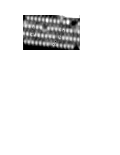
one possible interpretation of Fig. 3. The explanation is complicated by the fact that the surface atoms are obviously rearranged, at least part of them. Hence, it is not clear whether the surface periodicity is at all comparable to the bulk crystal structure. These surface modifications may occur naturally, or they might be induced by the applied cleaving procedure fischer:07 .
Atomically resolved images were obtained on areas up to , revealing narrow terraces of various lattice planes. Larger flat terraces, reflecting the unperturbed crystal structure, were not observed. A surface that differs substantially from the bulk structure may have completely different properties. In particular, SC may be suppressed close to the crystal surface. A modified surface structure might, therefore, hinder the reproducible observation of SC–derived changes to the density of states by STS. Similar arguments might apply to the case of CeCoIn since it has the same tetragonal crystal structure as its Ir counterpart. Possibly, one might even encounter similar difficulties in other HF superconductors. Therefore, dedicated surface preparation methods may have to be developed for each material in order to overcome such cleaving–related problems.
IV Conclusions
In conclusion, we reported on systematic investigation of in situ cleaved CeMIn, M = Co, Ir, single crystals by means of low–temperature STM/STS. A gap detected in CeCoIn is compatible with symmetry of the superconducting order parameter. The persistence of the gap beyond might evidence a precursor state to SC, similar to the pseudogap observed in underdoped cuprates. Atomically resolved topography imaging reveals a rearrangement of the surface atoms in CeIrIn. This modification might influence the tunneling spectroscopy not only in this compound, but also in CeCoIn or even in other HF superconductors.
V Acknowledgement
Work in Dresden was supported by the DFG research unit 960 ”Quantum phase transitions”. Z. F. acknowledges support through NSF-DMR-071042.
References
- (1) H. Hegger et al., Phys. Rev. Lett. 84, 4986 (2000).
- (2) C. Petrovic et al., Europhys. Lett. 53, 354 (2001).
- (3) C. Petrovic et al., J. Phys.: Condens. Matter 13, L337 (2001).
- (4) J. L. Sarrao and J. D. Thompson, J. Phys. Soc. Jpn. 76, 051013 (2007).
- (5) F. Steglich et al., Phys. Rev. Lett. 43, 1892 (1979).
- (6) S. Schmitt-Rink et al., Phys. Rev. Lett. 57, 8575 (1986).
- (7) D. J. Scalapino et al., Phys. Rev. B 34, 8190 (1986).
- (8) N. D. Mathur et al., Nature 394, 39 (1998).
- (9) K. Izawa et al., Phys. Rev. Lett. 87, 057002 (2001).
- (10) A. Vorontsov and I. Vekhter, Phys. Rev. Lett. 96, 237001 (2006).
- (11) Y. Kohori et al., Phys. Rev. B 64, 134526 (2001).
- (12) C. Stock et al., Phys. Rev. Lett. 100, 087001 (2008).
- (13) Y. Kasahara et al., J. Phys. Conf. Ser. 150, 052097 (2009).
- (14) Y. Nagajima et al., J. Phys. Soc. Jpn. 76, 024703 (2007).
- (15) Omicron NanoTechnology GmbH, Taunusstein, Germany.
- (16) S. Ernst et al., Sci. Technol. Adv. Mater. 8, 347 (2007).
- (17) Epoxy Technology, Inc. H21D, and UHU plus endfest 300.
- (18) H. Won and K. Maki, Phys. Rev. B 49, 1397 (1994).
- (19) R. C. Dynes et al., Phys. Rev. Lett. 41, 1509 (1978).
- (20) B. Dóra and A. Virosztek, Eur. Phys. J. B 22, 167 (2001).
- (21) G. Goll et al., Acta Phys. Pol. B 34, 575 (2003).
- (22) P. M. C. Rourke et al., Phys. Rev. Lett. 94, 107005 (2005).
- (23) W. K. Park et al., Phys. Rev. B 72, 052509 (2005).
- (24) C. Renner et al., Phys. Rev. Lett. 80, 149 (1997).
- (25) V. A. Sidorov et al., Phys. Rev. Lett. 89, 157004 (2002).
- (26) S. Nair et al., Phys. Rev. Lett. 100, 137003 (2008).
- (27) S. Kawasaki et al., Phys. Rev. B 65, 020504 (2002).
- (28) Ø. Fischer et al., Rev. Mod. Phys. 79, 353 (2007).