Thickness-dependent spontaneous dewetting morphology of ultrathin Ag films
Abstract
We show here that the morphological pathway of spontaneous dewetting of ultrathin Ag films on SiO2 under nanosecond laser melting is found to be film thickness dependent. For films with thickness h between nm, the morphology during the intermediate stages of dewetting consisted of bicontinuous structures. For films nm, the intermediate stages consisted of regularly-sized holes. Measurement of the characteristic length scales for different stages of dewetting as a function of film thickness showed a systematic increase, which is consistent with the spinodal dewetting instability over the entire thickness range investigated. This change in morphology with thickness is consistent with observations made previously for polymer films [A. Sharma et al, Phys. Rev. Lett., v81, pp3463 (1998); R. Seemann et al, J. Phys. Cond. Matt., v13, pp4925, (2001)]. Based on the behavior of free energy curvature that incorporates intermolecular forces, we have estimated the morphological transition thickness for the intermolecular forces for Ag on SiO. The theory predictions agree well with observations for Ag. These results show that it is possible to form a variety of complex Ag nanomorphologies in a consistent manner, which could be useful in optical applications of Ag surfaces, such as in surface enhanced Raman sensing.
1Department of Physics, Washington University in St. Louis, MO 63130
2Department of Material Science and Engineering, University of Tennessee, Knoxville, TN 37996
3Department of Mathematics, Western Kentucky University, Bowling Green, KY 42101
4Department of Chemical and Biomolecular Engineering, University of Tennessee, Knoxville, TN 37996
5Sustainable Energy Education and Research Center, University of Tennessee, Knoxville, TN 37996
1 Introduction
Silver (Ag) films and nanostructures have strong plasmonic activity and consequently, are very useful in the chemical detection of species via surface enhanced Raman scattering (SERS) [1, 2]. It is known that the magnitude of the localized field enhancement leading to increase in Raman scattering is very sensitive to the roughness or asymmetry (aspect ratio) of the nanostructures [3]. Therefore, controlling the morphology and nanostructure characteristics, of metals like Ag, in a reliable and cost-effective manner is very important towards further improving the sensitivity and selectivity of SERS detection.
One potential approach towards creating complex nanomorphologies in metals is to utilize the spontaneous dewetting of thin films [4, 5, 6, 7, 8, 9]. In the classical spinodal dewetting instability, an initially smooth film is unstable to height fluctuations because attractive intermolecular forces can exceed the stabilizing effect of interfacial tension [10, 11, 4]. As a result, a narrow band of wavelengths can spontaneously grow, eventually leading to film rupture and, more importantly, to morphologies with well-defined length scales [12, 13]. One of the important observations in polymer dewetting is the behavior of the dewetting morphology as the film progresses from its initially smooth state to a final stable state of particles. It has been observed that below a transition thickness , the intermediate stage dewetting morphology consists of bicontinuous structures, while above, it consists of regularly sized holes [14, 15]. This change in morphology has been attributed to the form of the intermolecular forces influencing dewetting [13]. Specifically, for ultrathin films, with thickness between 1 and 20 nm, the film thickness-dependent intermolecular forces are made up of a long range attractive component, and a shorter-range repulsive component. The transition thickness can be identified from the thermodynamic free energy of the system and, as shown by Sharma and Khanna [13], is located at the minimum in the curvature of the free energy. Consequently, the appearance of bicontinuous structures is correlated with films whose initial thicknesses lie to the left of the curvature minimum, while the formation of holes occur in films with thicknesses to the right of the minimum. In polymers, the the magnitude of is found to be of the order of a few nm’s. More importantly, knowledge of this transition can help guide the controlled fabrication of materials with different morphologies and length scales.
Recently, detailed investigations by various authors have shown that nanosecond laser irradiation of ultrathin metal films on non-wetting substrates can initiate a similar dewetting instability, producing robust and repeatable patterns with well-defined length scales [16, 6, 17, 7, 18]. Previously reported articles also showed that metal films can have different morphologies, including bicontinuous structures or holes, and in the case of Co on SiO the transition was found to occur between 3 to 4 nm in film thickness [19, 20]. In this work, we have explored the dewetting pathway for Ag metal on SiO substrates in the thickness range of nm under pulsed laser melting. Besides the numerous applications associated with Ag nanostructures, another important reason to choose Ag for this dewetting morphological study is that nanosecond laser heating effects do not introduce any novel dewetting effects, due primarily to the large thermal conductivity of Ag [18]. To capture the various morphologies between the flat film and the final nanoparticle state, the dewetting was investigated as a function of number of pulses. We observed that Ag shows the bicontinuous morphology up to a thickness of ~9.5 nm, while above that it shows holes. Moreover, measurements of the characteristic length scale showed the expected behavior associated with spinodal dewetting over the entire thickness range investigated. Importantly, the experimentally observed transition thickness agrees well with the value predicted by using the sum of possible intermolecular forces for Ag on SiO, and is analogous to results for polymer films. The results from dewetting of Ag films show that various complex morphologies, potentially useful towards plasmonic and non-linear optical properties, can be robustly fabricated in a repeatable and controllable manner.
2 Experimental Details
Ag films with thickness from 2 to 20 nm were deposited in high vacuum ( Torr) by pulsed laser deposition at room temperature onto commercially obtained, optical quality, wafers consisting of nm thick thermally grown oxide layer on polished wafers [17]. The deposition rate was typically nm/min. The energy dispersive X-ray spectrometry (EDS) was used to measure the Ag counts of the deposited films in a scanning electron microscope (SEM). The EDS counts were converted into an equivalent thickness value by using calibration based on step-height measurements of the film thickness. For every film thickness we measured the surface roughness via atomic force microscopy (AFM) and established an upper limit of nm for the average root mean square (RMS) roughness over the entire thickness range. Following the deposition, the films were irradiated in vacuum by a varying number of pulses n from a nm ultraviolet laser having a pulse length of 9 ns. Irradiation was at normal incidence by an unfocused laser beam of area mm at a repetition rate of 50 Hz. Under these vacuum deposition and irradiation conditions, the film surface was never exposed to air and hence no role of oxygen or an oxide layer was expected. The dewetting morphology was investigated as a function of film thickness , and the number of pulses , which typically ranged between 10 to 10,500 pulses, for irradiation at laser energies at or just above the melt threshold of the films. We have shown earlier that the melt threshold energy is a function of the film thickness [20]. For each thickness the melt threshold was determined by a visible roughening of the metal film surface, as detected under high-resolution SEM within the longest time scale of the experiment (i.e. after laser pulses) [21]. The range of used for the thickness regime investigated here was mJ/cm. For this irradiation condition, the heating and cooling rate of the metal film was of the order of K/s with a total heating plus cooling time per pulse of ns, which was much smaller than the spacing between pulses of ms. Consequently, as we have quantitatively shown earlier [22], negligible contribution to the morphology evolution was expected from processes in the solid state. Hence, any morphology changes occurred primarily during the liquid phase following each pulse. We also confirmed by EDS measurements that the laser irradiation did not result in substantial evaporation of the Ag, even after the longest irradiation experiments of 10,500 pulses.
3 Results and discussion
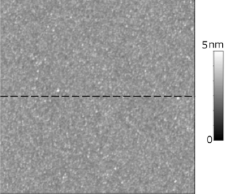
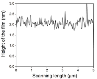
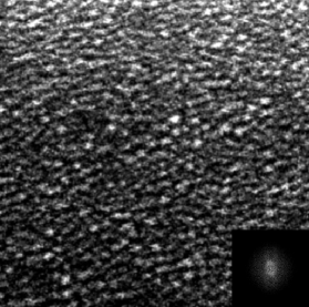
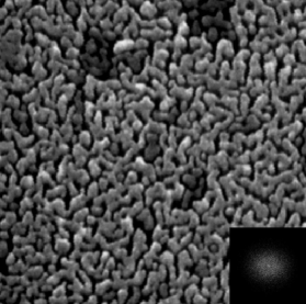
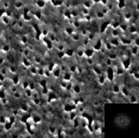
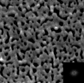
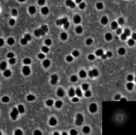
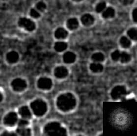
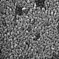
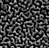
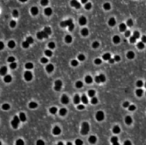
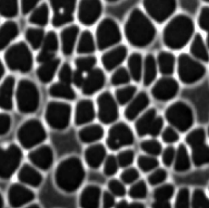
Figure 1(a) shows the AFM micrograph of as-deposited 2 nm Ag film on SiO substrate. The average RMS roughness of the film was measured by plotting the profile of the film along a horizontal dashed line (see Fig. 1(a)), which is shown in Fig. 1 (b), indicating RMS roughness to be 0.50.05 nm. Similar measurements were made for all the films investigated. In Fig. 2 (a-f), a series of SEM images denoting the early stage dewetting morphology, following irradiation by 10 laser pulses, is shown for a different Ag film thickness. The important evidence from this series of images is the distinct transition in the general nature of the morphology between the 9.5 and 11.5 nm films. Up to 9.5 nm [Fig. 2(a-d)], the morphology generally consists of asymmetric undulations or a bicontinuous type structure. On the other hand, for the 11.5 and 20 nm films [Fig. 2(e-f)], regular holes are clearly visible. Quantitative information about the spatial characteristics of these morphologies was obtained by evaluating the fast Fourier transform (FFT) of the SEM image contrast, which is related to the dewetting film’s height variations. The resulting FFT information of the contrast correlation is shown in the inset of each figure, and the important information here is the annular form for each of the films. This annular FFT is indicative of a narrow band of characteristic length scales for the height variations on the surface. This is an important observation given that the dewetting morphology can progress via either of the three pathways: homogeneous nucleation, heterogeneous nucleation, or spinodal dewetting [23]. In the case of homogeneous nucleation, the features are randomly distributed, both spatially, and in time, and no characteristic length scale should appear in this type of dewetting [24]. Heterogeneous nucleation can occur due to defects, impurities or other experimentally imposed heterogeneities. In this type of dewetting, a characteristic length scale could appear at the early stages of dewetting only in the presence of available ordered nucleation sites. However, we have not observed spatially ordered heterogeneities on the substrate surface, as well as on the as-deposited films, prior to irradiation. Therefore, the results presented here point strongly to the third option, which is spinodal dewetting [25].
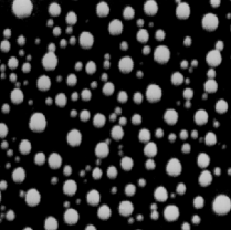
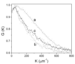
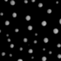
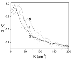
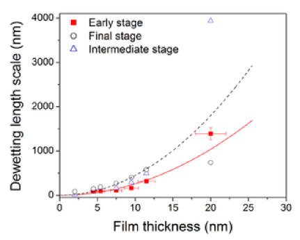
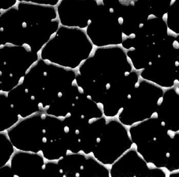
The characteristic length scale associated with spinodal dewetting is established at the very early stages of film deformation [4]. The early stage undulations, which occur prior to the appearance of large height variations in the film, are extremely difficult to capture experimentally. However, the subsequent morphology, which is a result of ripening of the initial undulations, forms as dewetting progresses and has length scales directly related to the initial length scale. Therefore, as shown by many authors, the final nanoparticle length scale, can be used as a measure of the thickness-dependent behavior [11, 6]. Here, the length scales were measured at different stages of the dewetting process as a function of film thickness. In Fig. 3(a-c), the progression of the morphology is shown for the 4.5 nm film, while Fig. 3(e-g) shows the same for the 11.5 nm films as a function of laser pulses between 10 and 10,500 shots. Figures 3(d) and (h) are the radial distribution functions (RDF) for each stage for the 4.5 and 11.5 nm film, respectively. From the position of the peaks in such RDF measurements, obtained directly from the FFT’s, it was possible to generate the characteristic length scale present in the pattern at each stage. The result of measuring length scales from these progressions is shown in Fig. 4(a). The early stage behavior is shown by the closed squares, the intermediate stage is shown by open triangles, while the final nanoparticle state is shown by open circles. One important observation from this measurement is that no dramatic change in length scale is seen when the morphology changes from the bicontinuous to the hole structures, i.e. between 9 to 11 nm. This strengthens the argument that both morphologies can arise for spinodal dewetting of Ag. Since the characteristic length scale for spinodal dewetting is known to vary as , we have also plotted trend lines for the early stage (solid line) and nanoparticle stage (dotted line) data sets with an trend. The early stage dewetting agrees reasonably well with the spinodal trend over the regime investigated, confirming a previously reported result for Ag, based on the behavior of the nanoparticle state [18]. An important observation can be made on the apparent deviation of the intermediate and final stage length scales for the thickest film investigated, i.e. the 20 nm film. The nanoparticle length appears much smaller than the trend (dotted line), while the intermediate state appears much larger. This can be understood as follows. The drop in the nanoparticle length scale is due to the nearest-neighbor interparticle spacing being dominated by a Rayleigh-like break-up of the arms of the polygon, as shown in Fig. 4(b). In contrast, particles in the 11.5 nm film form at the vertex of the polygons formed during the dewetting stage [Fig. 3(g)]. A similar argument, based on a change in the feature shape being measured, is likely to explain the intermediate state behavior. As shown in Fig. 3(e-g), the progression of the hole morphology is through merging of the holes into polygons, whose size (diameter) will be dependent upon the number of holes it was formed from. It is quite likely that the large increase in length scale for the intermediate state of the 20 nm film is because the measured length scale is for polygons formed from numerous holes.
The above results provide a strong case for Ag dewetting via the spinodal process, with additional support coming from that fact that similar morphological characteristics are observed when polymer films dewet by the spinodal instability. As mentioned in the introduction, polymer films have been observed to have a bicontinuous to hole transition at thicknesses of a few nm and the theoretical position of this thickness has been correlated to the nature of the free energy [13, 15]. Specifically, the location of minima in the free energy curvature has been correlated to this transition thickness. To determine if a similar behavior is seen for the Ag metal, a sum of different types of attractive and repulsive intermolecular interactions have been used to estimate the free energy and its curvature as a function of thickness h for Ag on SiO. Since the films are very thin, we have neglected the gravitational term in our calculations.
3.1 Free energy analysis to determine transition thickness
The intermolecular interaction free energy of a uniform thin film can be realized by first describing the disjoining pressure acting on a film. Consider a liquid film of height on top of a flat substrate. The thickness dependent disjoining pressure, , can be expressed by adding a long-range attractive (Van der Waals interaction) and a short range repulsive interaction between the various interfaces formed as a result of having the film on a substrate. The repulsive term typically consists of two parts: (i) a Lennard-Jones (L-J) type repulsion [26] which appears due to the electron cloud interaction, and (ii) an electrostatic force, which is a result of electric layers forming at the liquid-substrate interface.
The total disjoining pressure, by considering a long-range attraction, a short range repulsion expressed as a Lennard-Jones type form [26], and the electrostatic force [13, 26], is given by:
| (1) |
Here, A is the Hamaker coefficient, which has a negative value in units of Joule, and is the critical length at minimum . is the spreading coefficient which is related to the magnitude of electrostatic part of the disjoining pressure, and is a correlation (or Debye) length. Using Eq. 1, the free energy density (energy/area) of a uniform film can be written as:
| (2) |
where, is defined as:
| (3) |
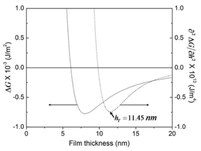
and (the transition thickness) is calculated from the position of the minimum in the free energy curvature as:
| (4) |
The above analysis was performed for Ag on SiO substrate, and the correlation length was taken to be in the range of nm [27]. The values of the constants used in the analysis for Ag are given in Table 1. Table 1 also consists of material parameters for few other metals of interest, where the value of is estimated by considering that lies between 0.2 to 1 nm. The typical transition thickness () calculated using Eq. 4 for Ag appears to be between 0.3 and 11.45 nm. The free energy and curvature plots using Eq. 2 and 4 and the correlation length nm for Ag are shown in Fig. 5. With this result we can make the following observations. In polymer films, the bicontinuous structures are observed for the thinner films, while holes are observed in the thicker ones. Similarly, for the presented case of Ag films on SiO substrate, the bicontinuous structures are obtained for films nm, while above this thickness the morphology evolution starts with the formation of holes. This experimental result matches well with the theoretical prediction of 11.45 nm, provided a correlation length of nm is used.
4 Conclusion
In conclusion, we have investigated the morphology evolution in nanometer thick Ag films under melting by nanosecond laser pulses. The initial dewetting morphology is found to be a bicontinuous morphology for films with thickness 9.5 nm, while discrete holes appear for films with thickness > 11.5 nm. Evaluation of the characteristic dewetting length scales indicated a good agreement with a trend, which was evidence for the spinodal dewetting instability. The observations of the different morphologies and a transition thickness is consistent with the behavior observed previously for polymer films. The experimentally observed transition value for Ag, of between 9.5 - 11.5 nm, agrees well with predictions from intermolecular forces. This work shows that complex and controllable morphologies can be obtained for Ag, but more insight is needed to understand the physical origins of dewetting pattern morphologies in thin metal films.
RK acknowledges support by the National Science Foundation through CAREER grant DMI- 0449258, grant NSF-DMR-0856707, and grant NSF-CMMI-0855949. M.K. acknowledges WKU awards 10-7016 and 10-7054.
References
- [1] M. Quinten, A. Leitner, J. Krenn, and F. Aussenegg, “Electromagnetic energy transport via linear chains of silver nanoparticles,” Opt. Lett., vol. 23, p. 1331, 1998.
- [2] K. Willets and R. P. Van Duyne, “Localized Surface Plasmon Resonance Spectroscopy and sensing,” Annu. Rev. Phys. Chem., vol. 58, p. 267, 2007.
- [3] M. Fleischmann, P. J. Hendra, and A. MacQuillan, “Raman spectra of pyridine adsorbed at a silver electrode,” Chem. Phys. Lett., vol. 26, pp. 163–168, 1974.
- [4] S. Herminghaus, K. Jacobs, K. Mecke, J. Bischof, A. Fery, M. Ibn-Elhaj, and S. Schlagowski, “Spinodal dewetting in liquid crystal and liquid metal films,” Science, vol. 282, pp. 916–919, 1998.
- [5] A. Atena and M. Khenner, “Thermocapillary effects in driven dewetting and self assembly of pulsed-laser-irradiated metallic films,” Physical Review B (Condensed Matter and Materials Physics), vol. 80, no. 7, p. 075402, 2009.
- [6] C. Favazza, R. Kalyanaraman, and R. Sureshkumar, “Robust nanopatterning by laser-induced dewetting of metal nanofilms,” Nanotechnology, vol. 17, pp. 4229–34, 2006.
- [7] J. Trice, C. Favazza, D. Thomas, H. Garcia, R. Kalyanaraman, and R. Sureshkumar, “Novel self-organization mechanism in ultrathin liquid films: theory and experiment,” Phys. Rev. lett., vol. 101, no. 1, p. 017802, 2008.
- [8] Y. F. Guan, R. C. Pearce, A. V. Melechko, D. K. Hensley, M. L. Simpson, and P. D. Rack, “Pulsed laser dewetting of nickel catalyst for carbon nanofiber growth,” Nanotechnology, vol. 19, p. 235604, 2008.
- [9] J. Boneberg, A. Habenicht, D. Benner, M. Leiderer, Trautvetter, C. Pfahler, A. Plettl, and P. Ziemann, “Jumping nanodroplets: a new route towards metallic nano-particles,” Appl. Phys. A: Mater. Sci. and Proc., vol. 93, pp. 415–419, 2008.
- [10] A. Vrij, “Possible mechanism for the spontaneous rupture of thin, free liquid films,” Discuss. Faraday Soc., vol. 42, pp. 23–27, 1966.
- [11] G. Reiter, “Dewetting of thin polymer films,” Phys. Rev. Lett., vol. 68, no. 1, pp. 75–78, 1992.
- [12] F. Brochard Wyart and J. Daillant, “Drying of solids wetted by thin liquid films,” Can. J. Phys., vol. 68, pp. 1084–88, 1990.
- [13] A. Sharma and R. Khanna, “Pattern Formation in Unstable Thin Liquid Films,” Phys. Rev. Lett., vol. 81, pp. 3463–66, 1998.
- [14] R. Xie, A. Karim, J. Douglas, C. Han, and R. Weiss, “Spinodal dewetting of thin polymer films,” Phys. Rev. Lett., vol. 81, pp. 1251–1254, AUG 10 1998.
- [15] R. Seemann, S. Herminghaus, and K. Jacobs, “Gaining control of pattern formation of dewetting liquid films,” J. Phys. Cond. Matt., vol. 13, pp. 4925–4938, MAY 28 2001.
- [16] J. Bischof, D. Scherer, S. Herminghaus, and P. Leiderer, “Dewetting modes of thin metallic films: nucleation of holes and spinodal dewetting,” Phys. Rev. Lett., vol. 77, no. 8, pp. 1536–1539, 1996.
- [17] C. Favazza, J. Trice, H. Krishna, R. Kalyanaraman, and R. Sureshkumar, “Laser-induced short- and long-range ordering of Co nanoparticles on SiO2,” Appl. Phys. Lett., vol. 88, pp. 1531181–83, 2006.
- [18] H. Krishna, N. Shirato, C. Favazza, and R. Kalyanaraman, “Energy driven self-organization in nanoscale metallic liquid films,” Phys. Chem. Chem. Phys., vol. 11, p. 8136, 2009.
- [19] C. Favazza, J. Trice, R. Kalyanaraman, and R. Sureshkumar, “Self-organized metal nanostructures through laser-interference driven thermocapillary convection,” Appl. Phys. Lett., vol. 91, p. 043105, 2007.
- [20] J. Trice, D. G. Thomas, C. Favazza, R. Sureshkumar, and R. Kalyanaraman, “Investigation of pulsed laser induced dewetting in nanoscopic Co films: Theory and experiments,” Phys. Rev. B, vol. 75, p. 235439, 2007.
- [21] C. Favazza, J. Trice, A. Gangopadhyay, H. Garcia, R. Sureshkumar, and R. Kalyanaraman, “Nanoparticle ordering by dewetting of Co on SiO2,” J. Elec. Mat., vol. 35, pp. 1618–20, 2006.
- [22] C. Favazza, R. Kalyanaraman, and R. Sureshkumar, “Dynamics of ultrathin metal films on amorphous substrates under fast thermal processing,” J. Appl. Phys., vol. 102, p. 104308, 2007. In press, Available at www.arxiv.org: paper-id: cond-mat/0703016.
- [23] P.-G. de Gennes, F. Brochard-Wyart, and D. Quere, Capillarity and wetting phenomenon. New york: Springer, 2003.
- [24] T. Stange and D. Evans, “Nucleation and growth of defects leading to dewetting of thin polymer films,” Langmuir, vol. 13, pp. 4459–4465, 1997.
- [25] U. Thiele, M. Mertig, and W. Pompe, “Dewetting of an evaporating thin liquid film: heterogeneous nucleation and surface instability,” Phys. Rev. Lett., vol. 80, no. 13, pp. 2869–2872, 1998.
- [26] V. Mitlin, “On dewetting conditions,” Colloids Surf. A, vol. 89, pp. 97–101, 1994.
- [27] A. Sharma, “Relationship of thin film stability and morphology to macroscopic parameters of wetting in the apolar and polar systems,” Langmuir, vol. 9, no. 3, pp. 861–869, 1993.
- [28] H. M. Lu and Q. Jiang, “Surface tension and its temperature coefficient for liquid metals,” J. Phys. Chem., vol. 109, pp. 15463–15468, 2005.
- [29] A. Sharma, “Relationship of thin film stability and morphology to macroscopic parameters of wetting in the apolar and polar systems,” Langmuir, vol. 9, no. 3, pp. 861–869, 1993.
- [30] J. Israelachvili, Intermolecular and surface forces, ch. van der Waals forces between surfaces. London, UK: Academic Press, 1992.
| Metal | (J-m) [28] | (degree) | (J-m) [29] | (J) [30] | using Eq. 3 (nm) | using Eq. 4 (nm) |
|---|---|---|---|---|---|---|
| Ag | 0.925 | 82 | 0.79 | -1.33x10 | 0.300 | 0.3 - 11.45 |
| Au | 1.145 | 88 | 1.11 | -1.76x10 | 0.293 | 0.29 - 11.92 |
| Co | 1.882 | 101 | 2.26 | -3.1x10 | 0.273 | 0.27 - 12.10 |
| Cu | 1.304 | 92 | 1.35 | -2.08x10 | 0.288 | 0.29 - 11.62 |
| Fe | 1.870 | 101 | 2.24 | -2.9x10 | 0.265 | 0.26 - 11.88 |
| Mn | 1.152 | 88 | 1.12 | -8.12x10 | 0.019 | 2.64 - 19.23 |
| Ni | 1.781 | 100 | 2.10 | -9.9x10 | 0.160 | 1.13 - 13.47 |
| Pt | 1.746 | 100 | 2.04 | -2.56x10 | 0.259 | 0.26 - 11.94 |
| Ti | 1.525 | 96 | 1.69 | -4.32x10 | 0.372 | 0.37 - 10.72 |
| V | 1.770 | 100 | 2.08 | -1.74x10 | 0.212 | 0.21 - 12.58 |