Analysis of optical properties of strained semiconductor quantum dots for electromagnetically induced transparency
Abstract
Using multiband theory we study the size and geometry dependence on the slow light properties of conical semiconductor quantum dots. We find the -type scheme for electromagnetically induced transparency (EIT) to be most favorable, and identify an optimal height and size for efficient EIT operation. In case of the ladder scheme, the existence of additional dipole allowed intraband transitions along with an almost equidistant energy level spacing adds additional decay pathways, which significantly impairs the EIT effect. We further study the influence of strain and band mixing comparing four different band structure models. In addition to the separation of the heavy and light holes due to the biaxial strain component, we observe a general reduction in the transition strengths due to energy crossings in the valence bands caused by strain and band mixing effects. We furthermore find a non-trivial quantum dot size dependence of the dipole moments directly related to the biaxial strain component. Due to the separation of the heavy and light holes the optical transition strengths between the lower conduction and upper most valence-band states computed using one-band model and eight-band model show general qualitative agreement, with exceptions relevant for EIT operation.
pacs:
73.21.La, 78.67.Hc, 42.50.GyI Introduction
InAs/GaAs quantum dot structures have recently received much attention due to their relevance for optoelectronic devices. Piprek (2007) The discrete level nature of quantum dots offer important advantages over bulk and quantum well material for applications in conventional devices like lasers and optical amplifiers, as well as devices for all-optical signal processing. However, quantum dots also give the possibility of realizing solid-state implementations of effects and functionalities so far only demonstrated in atomic systems. For instance, the practical exploitation of slow light effects such as electromagnetically induced transparency (EIT) demonstrated in ultracold atoms Hau et al. (1999) is naturally pursued using quantum dots. Chang-Hasnain et al. (2003) Important aspects in this context are to accurately model the optical properties of the quantum dots and to consider the influence of the lattice mismatch induced strain field and its effects on the bandstructure and eigenstates. Apart from Refs. [Michael et al., 2006; Chow et al., 2007] that focus on the many-body aspects of EIT operation most theoretical investigations of EIT induced slow light Kim et al. (2004); Jänes et al. (2005); Nielsen et al. (2007); Lunnemann and Mørk (2009) have been based on simple quantum dot models that do not take into account important contributions from e.g. biaxial strain.
In this paper, we use theoryKane (1966); Dresselhaus et al. (1955) to determine the bandstructure of conical quantum dots. A first popular multiband calculation scheme for bulk materials is due to Luttinger and Kohn Luttinger (1956); Luttinger and Kohn (1955) which later on was extended to heterostructures by an ad hoc symmetrization procedure.Bastard (1988) In order to overcome this ad hoc procedure, Burt formulated the so-called exact envelope function method Burt (1992, 1994) and soon after ForemanForeman (1993) used this method to derive a six-band model for the valence bands of zincblende heterostuctures. Pokatilov et al.Pokatilov et al. (2001) have provided an eight-band model for the conduction and the valence bands. They studied quantum dots using a spherical approximation and compared their model, based on exact envelope-function theory, against the usual symmetrized approach. The asymmetry parameter present in the Burt-Foreman formalism but not in the Luttinger-Kohn formalism is shown to lead to changes of approximately meV in the electronic bandstructures of InAs/GaAs. Pokatilov et al. (2001)
Optoelectronic properties of InGaAs zincblende quantum-dot with varying shape and size based on theory have already been studied by Schliwa et al.Schliwa et al. (2007) and Veprek et al..Veprek et al. (2008) However, so far, only a small selection of all possible transitions have been studied. In this work we apply the eight-band model based on Burt-Foreman formalism derived in Ref. [Pokatilov et al., 2001] to zincblende InAs/GaAs conical quantum dots. We choose the conical geometry because (i) it introduces important symmetry lowering effects not present in the earlier spherical models, and (ii) it mimicks closely the structures realized in experimental systems, e.g., in Ref. [Inoue et al., 2008]. We study the size and shape dependence. In particular, we show that some of the, for EIT yet unexplored, interband transitions are highly relevant. Furthermore, we investigate the effect of strain and band-mixing between the conduction band and valence bands by comparing four different models. Although the previous bandstructure studies do include these effects, their impact on optical properties, such as EIT, have not yet been investigated.
The paper is organized as follows. In Sec. II the theory for EIT, bandstructure calculations and dipole moments is introduced. In Sec. III we present results for the bandstructure and dipole moments calculations, addressing the volume and shape effects, while in Sec. IV these results are used to develop level schemes that lead to an efficient EIT operation. The paper is concluded in Sec. V.
II Theory
II.1 EIT
EIT refers to an artificially created spectral region of transparency in the middle of an absorption line due to the destructive quantum interference arising from two transitions in a three-level system.Harris et al. (1990); Harris (1997) By virtue of the Kramers-Krönig relations a dip in absorption is accompanied by a large positive slope of the refractive index which translates into a reduced group velocity in vicinity of the resonance. Experimental realization of EIT in semiconductor structures has been achieved for the case of quantum wells Ref. [Serapiglia et al., 2000; Philips and Wang, 2004; Kang et al., 2008], whereas for quantum dots (QDs), to the best of our knowledge, only two reports exist.Marcinkevičius et al. (2008); Ma et al. (2009)
EIT effects in quantum dots and wells have mostly been studied using models that are rooted in atomic physics assuming an archetypical EIT configuration in an ideal medium.Chang-Hasnain et al. (2003); Kim et al. (2004); Jänes et al. (2005); Nielsen et al. (2007) These models truncate the number of active levels in the system to consider only the 3 levels being addressed by the laser fields. The generic EIT setup relies on a coupling and a probe laser driving separate transitions (see Fig. 1). In case of the -scheme, the ground state has the same parity as state , and the transition is thereby dipole forbidden. State is of the opposite parity and dipole coupled to both and . An intense near resonant continuous wave electromagnetic field, termed the coupling field, drives the - transition. Another also near resonant, but much weaker probe field, is applied to the - transition.
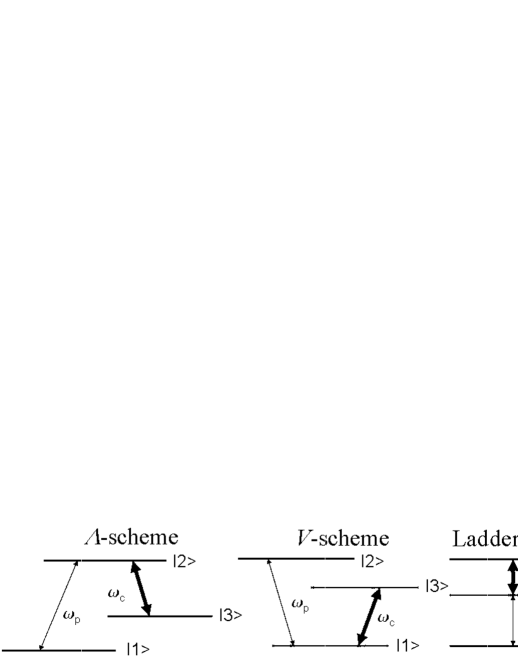
The archetypical EIT schemes are native to the atomic physics literature and generally one seeks to avoid excitation of carriers. In semiconductors such non-carrier exciting schemes involve a interband probe transition along with an intraband coupling transition. The frequency for the coupling field lies within the deep infrared, a range for which high intensity laser operation is very difficult. Carrier exciting schemes on the other hand involve two interband transitions, where the coupling field is effectively pumping carriers into the conduction band. The carriers interact via the Coulomb force, EIT schemes of this kind have been shown to be favorable when the effect of such many-body interactions are included.Houmark et al. (2009); Michael et al. (2006); Chow et al. (2007)
The study of pulse propagation in a semiconductor slow light medium generally involves solving the coupled Maxwell-Bloch equations (see e.g. Ref. [Nielsen et al., 2009]). However, under certain circumstances an analysis of the steady state properties of the semiconductor Bloch equations (SBE) alone is adequate. Houmark et al. (2009) If this is the case then the linear optical response extracted via the SBE will be directly linked to the propagation characteristics of a wavepacket traveling in an optically thick system.
A relevant figure of merit for slow light operation is the slowdown factor , which is defined as the ratio of the velocity of light in vacuum to the group velocity of a wavepacket traveling through the slow light medium:
| (1) |
where is the speed of light in vacuum, and is the refractive index, with being the background permittivity and the susceptibility of the active material. The maximum slowdown is found at the frequency for which the slope of the refractive index is largest. Notice that the slowdown factor obtained away from resonance () is given by the background refractive index. The first order susceptibility, or linear system response, is found from the induced macroscopic polarization as , where is the vacuum permittivity and is the amplitude of the probe field. In turn the time resolved macroscopic polarization component in the direction of the probe field, , is computed from the microscopic polarizations according to semiclassical theory:Haug and Koch (1990)
| (2) |
where is the density matrix for localized dot states (). Dipole matrix elements are denoted , is the two-dimensional density of the dots in the growth plane, and is the thickness of the active region. Within the 3-level, (non-carrier exciting) approximation one can derive an analytical expression for the susceptibility (see e.g. Ref. [Chang-Hasnain et al., 2003]). When both fields are resonant with their respective transitions (), the slowdown factor and the absorption become:
| (3) | |||||
| (4) | |||||
where , , . is the intensity of the coupling beam, and are the dipole moments of the probe and coupling transition, respectively and and are the dephasing rates of the polarization components of the probe and the uncoupled non-radiative transition, respectively. The above expressions displays the significance of maximizing the transition strengths of the two light beams. In case of the slowdown factor the dipole moment of the probe transition determines the largest obtainable slowdown, while the dipole moment of the pump transition is related to the pump power required to reach this maximum. The absorption drops as .
II.2 Bandstructure
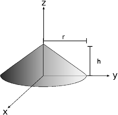
The dipole moments which govern the EIT characteristics are determined using eight-band theory including strain effects. We study the conical quantum dots shown in Fig. 2. The dot material is InAs and the barrier material is GaAs.
Both InAs and GaAs are zincblende materials so in order to reduce the problem to a two dimensional model we disregard anisotropy effects. This entails that we disregard phenomena such as piezoelectricity and atomistic anisotropic effects Fonoberov and Balandin (2003); Barettin et al. (2008). The atomistic anisotropic effects have been investigated by Bester and Zunger Bester and Zunger (2005) showing that they lead amongst other things to a splitting of states which in our model are degenerate. This splitting is however less pronounced for cylindrical shaped quantum dots as studied here. Recently it has been shown that second order piezoelectric terms effectively cancel linear piezoelectric effects for cylindrical shaped quantum dots. Bester et al. (2006a, b); Schliwa et al. (2007) We have checked the isotropic assumption and found a maximum error for the strain fields of along the axis, going rapidly to zero at the edges of the dot.
We investigate both the effect of strain and band mixing. The effect of band mixing is determined by comparing the eight-band results with one-band model results for the conduction band and the heavy holes. Due to the lattice mismatch present in the systems under consideration in this paper (InAs/GaAs quantum dots) the materials will be strained. In the eight-band model the wavefunction of the localized dot state is given by a linear combination of the eight Bloch states weighted by an envelope function,
| (5) |
where are the envelope function and are the Bloch states. We use the eight-band Hamiltonian described in Ref. [Pokatilov et al., 2001], while for the strain-dependent part we follow Ref. [Zhang, 1994].
In the following we explicitly present the one-band models as due to their simplicity these are most open to interpretation. The one-band eigenvalue equation for the envelope functions reads where , and are the Hamiltonian, the envelope wave function and the energy, respectively. denotes either the conduction band or the heavy holes, i.e., . The Hamiltonian is
| (6) |
where is the kinetic part, is the energy of the unstrained band edge, and is the strain dependent part. The solutions are spin degenerate in the one-band model, i. e., and , and and .
In the one-band model the strain Hamiltonian for a zincblende crystal structure is given by
| (7) | |||||
| (8) |
where () and are the conduction (valence)-band hydrostatic deformation potential and is the shear deformation potential, Bir and Pikus (1974) while the hydrostatic and biaxial strain components read
| (9) | |||||
| (10) |
where is the strain tensor. The strain fields are found by minimizing the elastic strain energy. Fonoberov and Balandin (2003)
II.3 Dipole moments
The momentum matrix element is given by:
| (11) |
where or 8. and are the envelope and the Bloch parts of the momentum matrix element, respectively. It is usual to consider only the Bloch part since the envelope part is usually an order of magnitude smaller. Stier et al. (1999)
As shown in Ref. [Burt, 1993], the evaluation of the momentum matrix element is meaningful while dipole matrix elements are ill-defined in crystals involving extended Bloch states. Thus, we first calculate and then use the relation between the momentum and the electric dipole matrix element given by Ref. [Merzbacher, 1961]
| (12) |
where , is the free electron mass and is the electronic charge.
For material parameters used in calculations we refer to Ref. [Meyer and Ram-Mohan, 2001].
III Results: bandstructure and dipole moments
The first results we present are related to a set of conical quantum dots where the aspect ratio between the radius and the height of the dot has been fixed so that . We focused on the first twelve bound states for both bands. Since all the states are at least doubly degenerate (spin degeneracy), we consider six energy levels (labeled from 1 to 6) for both bands. In the one-band model, due to the conical quantum-dot symmetry and isotropy assumption (giving an inversion symmetric model), level 2 and level 3 are degenerate for both the conduction and the valence band, level 4 and level 5 are degenerate for the valence band, and level 5 and level 6 are degenerate for the conduction band. In the upper part of Fig. 3 and Fig. 4 we show the energy levels and the most relevant interband dipole moments for EIT ( is also included due to its relevance for other applications) corresponding to a dot with nm for the four different models: one-band model without strain, one-band model with strain, eight-band model without strain and eight-band model with strain. Throughout this paper we consider only right-handed circularly polarized light.

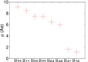
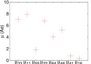

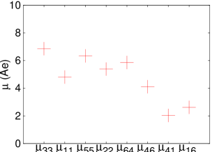
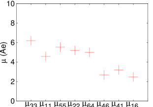
In Figs. 3 and 4 the thicknesses of the lines indicating the transitions are proportional to the corresponding dipole moments. Obviously, an eight-band model calculation leads to a higher valence-band density-of-states as compared to a one-band calculation. Hence, also more interband transitions result, in a given energy range, when using an eight-band model. We have chosen to show in the bottom part of Fig. 3 and Fig. 4 only the strongest eight dipole-matrix elements for both one-band and eight-band models. First, we observe that there is a qualitative agreement between dipole-moment results for the one-band and eight-band models with strain (Figure 4). This is due to the fact that in the eight-band model the biaxial strain component of Eq. (10) shifts heavy-holes (light-holes) to higher (lower) energies. As a consequence the valence-band groundstate and the first excited states are predominantly heavy-holes like giving rise to a general better agreement between the one-band model and the eight-band model. The only notable discrepancies are observed for the EIT relevant transitions and . Second, the inclusion of strain reduces the strength of the dipole moments significantly. This is because there is a non-trivial influence of strain on dipole moments. The conduction-band states are only affected by the hydrostatic strain component of Eq. (9) giving rise more or less to a constant shift in the effective potential inside the dot while the valence band states, in addition to the hydrostatic strain, are also affected by the biaxial strain component [see Eq. (10)]. The latter component is highly inhomogeneous inside the dot. In the eight-band model there is a third contribution from and strain components Zhang (1994) but this term is not as significant as the biaxial of Eq. (10).
In order to understand the influence of strain on the dipole moment we compare in Fig. 5 the valence-band groundstate probability density (eight-band model) with and without the influence of the strain field for a quantum dot with height nm and radius nm.
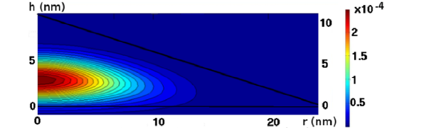
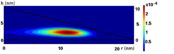
While in the case without strain the groundstate shows a s-like shape, the biaxial-strain component modifies the hole wave function into a toroidal shape moving it away from the center of the dot where the potential is stronger. This drastically reduces the overlap between the envelope functions of the conduction and valence band and consequently the corresponding dipole moments.
The reduction of the dipole moment due to strain is evident in Fig. 6 where we plot the interband dipole moment between the conduction- and the valence-band ground states for the four different models as a function of .

In the models with strain we have a maximum around nm while the dipole moments for the two models without strain grow monotonically with increasing height and eventually reach a plateau value corresponding to the bulk value of Åe. The monotonic increase of the dipole moments can be understood based on Eq. (12). Without strain the momentum matrix elements (mainly determined by ) remains constant with increasing height whereas the energy difference decreases. The presence of strain reduces the overlap of electron and hole distributions as a result of the increased displacement of the hole wavefunctions away from the center leading to the observed decrease in the dipole moments.

In Fig. 7 we plot the energies of the first six levels in the conduction (top) and valence band (bottom) as a function of the height . The wave functions of the confined states are characterized (in the eight-band model) by eight envelopes weighted differently depending on the state. As mentioned above, the biaxial strain is inhomogeneous and this, combined with the differently spatially distributed envelope functions, leads to a higher sensitivity against strain as compared to a one-band model. Further, the inhomogeneity of the strain field grows with volume, especially for the biaxial-strain component of Eq. (10). These coupled strain-band mixing effects lead to energy crossings in the valence band. We have also indicated where the wetting layer continuum starts (WL). The WL dashed lines in Fig. 7 are computed using a Ben-Daniel Duke approach for a 0.5 nm InAs quantum-well embedded in GaAs Bastard (1988). We observe that only the last three considered conduction-band levels for the smallest quantum dot lay above the lower bound of the wetting layer continuum states.

The most relevant dipole moments for EIT for the eight-band model are shown in the upper part of Fig. 8 as a function of . The bottom part gives the related energy differences . The strain reduces the dipole-moment strengths with increasing volume because of the decreasing wave function overlap (similar to what was found for ).
This geometry effect is indeed mainly a function of the dot volume as Fig. 9 shows. Here, we refer to a second set of quantum dots with different aspect ratios having the same volume . The interband dipole moments (top) and relative energy differences (bottom) are depicted as a function of and evidently results are rather insensitive to the aspect ratio.

IV Results: EIT
IV.1 3 level vs. many levels
In this section we consider right-handed circularly polarized light for both the coupling and probe fields and investigate the slow light characteristics upon propagation through several stacked layers of QD material. We assume that one can disregard propagation effects in the coupling field. In case of non-carrier exciting schemes, the coupling field is effectively connecting two empty states, thus rendering the transition transparent. In the case where the coupling beam is exciting carriers we consider a propagation through sufficiently thin device so that the coupling intensity remains constant. We use a lattice temperature of 200 K, for which the literature Borri et al. (1999, 2001) gives dephasing rates around . The system response is calculated using a procedure similar to Ref. [Houmark et al., 2009]. First we investigate a ladder-type scheme. The ladder scheme is generally non-carrier exciting. We consider a situation where the probe pulse connects the conduction band/valence band ground state () and the coupling beam is tuned to the intraband transition in the conduction band between the ground state - and first excited level. This particular setup has been the prime candidate for theoretical scrutinyChang-Hasnain et al. (2003); Nielsen et al. (2007) employing a three level approach along with a single band model including only hydrostatic strain. To illustrate the importance of including all energy levels and transitions along with a more detailed bandstructure calculation we show in Fig. 10 the imaginary part of the susceptibility calculated using a coupling intensity of for two dot sizes (height 7.5 nm and 9 nm, both ) using either the most simple model (one-band unstrained) or the most complex (eight-band strained).
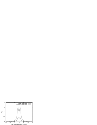


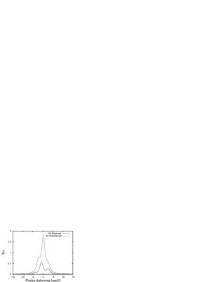
Most notably the EIT effect, which is recognized as a dip in the absorption spectrum symmetric around the probe frequency and is present in the simple three level models, is absent from three out of four multi-level calculations. The reason for this is that the additional level structure is dipole coupled to the three level EIT system. In the particular ladder configuration considered here, due to the relatively close spacing between the energy levels, higher lying states are also being addressed by the coupling field thereby adding alternative decay pathways that effectively destroy the destructive interference between the available paths, which is at the origin of EIT. In the one band unstrained calculation the energy levels are almost equidistantly spaced resulting in a peak in stead of a dip in the spectrum. The level structure is modified by strain and the inclusion of additional bandstructure, in fact the multi-level model for the dot of height indeed displays the EIT effect. In this particular case the higher lying shells are not in as close resonance with the coupling beam and a simple three level treatment is seen to produce similar results as the full multi-level model. The eight-band multi-level calculation for the larger dot () has reminiscence of the EIT effect but the spectrum is quite far from the ”ideal” spectrum predicted by the simple model. In general, ladder schemes in rotationally symmetric dots are, due to the near equidistantly spaced energy levels, likely subjected to the issue of the coupling beam being in resonance with other transitions. Carrier exciting or - schemes connecting only inter-band transitions are due to their larger transition energies much less likely to encounter this problem. Furthermore, the frequency range of inter-band transitions is much easier accessible to industry lasers, than the near infrared required by ladder-type schemes.
IV.2 Size/geometry dependence
The possible interband EIT schemes are illustrated in Fig. 4 (top). By combining the shown EIT relevant transitions a variety of different as well as -schemes can be accessed. As noted in a previous section there are very few differences between dipole moments predicted by the one-band strained model and the eight-band strained model, however the deviations that do exist, appears for transitions that could be used in connection with EIT. The one-band strained model significantly overestimates , a transition that would otherwise seem attractive to use for EIT. Furthermore is very small in all but the eight-band strained model. To illustrate the impact of these differences we have in Fig. 11 shown absorption spectra for an EIT scheme constructed using as probe and as coupling transition.

It is seen that using eight-band strained bandstructure results in an altered EIT behavior. The signature feature, the split peaks, are higher and closer together, a direct consequence of the magnitudes of the involved dipole moments. These significant differences between the spectra justifies focusing on the results of the more exact eight-band strained bandstructure model. A and scheme can be realized using as coupling transition and either of the two transitions or for the probe field. Two similar schemes can be accessed using the same probe transitions and for the coupling field. As is evident from Fig. 9 the dipole moments are relatively unchanged by varying shape (aspect ratio), we choose to focus on since the common probe transitions ( and ) are maximized for this geometry and consider volume dependencies.
We see that for small dots () the dipole moments addressed by the coupling beam are relatively small (on the order of ) and therefore dots of this size are not suitable for EIT operation. As the dot increases in size both coupling transitions become stronger, the two probe transitions, however begins to decrease. The dipole is always the smaller of the two probe transitions, and the fact that it drops off faster suggests that one should aim at using , ground state to ground state, as probe transition.
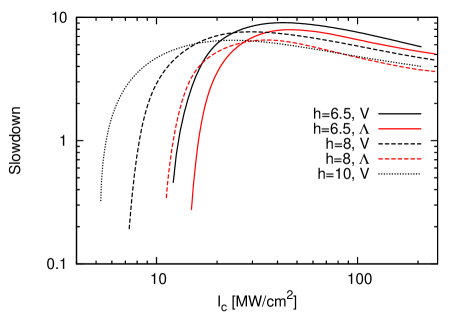
To quantify the above discussion we show in Fig. 12 the slowdown factor as a function of coupling intensity calculated for three different dot volumes () for each of the two remaining EIT schemes (for the dot, in the case of the scheme no EIT behavior is found due to its weak coupling transition. Slowdown results for this dot/EIT setup has therefore been omitted in Fig. 12.). For every dot type we see that the -scheme prevails, it has the lowest coupling power requirements and the largest obtainable slowdown value. The first observation can be understood from Fig. 8 where the -scheme coupling transition is always the larger. Since both schemes utilize the same probe transition one could be inclined to think that they should display the same maximum slowdown value. The reason they do not, is that the coupling beam, although detuned, is exciting carriers into the levels connected by the probe beam. The presence of the carriers serve to block the probe transition. As indicated in the lower part of Fig. 8, the coupling beam in the case is less detuned from the probe transition than in the V case, and thus more carriers are excited into the electron and hole ground states, resulting in a smaller effective probe transition strength. It is apparent that the best tradeoff between maximum slowdown and coupling intensity is found using the scheme for dots having a relatively large height, in the region around . In the literature the scheme has also been deemed preferable due to its ability to overcome inhomogeneous broadening,Lunnemann and Mørk (2009) and a favorable carrier redistribution mechanism.Houmark et al. (2009)
V Conclusion
For the investigated system we have shown that the strain field generally reduces optical transition strengths as a function of the volume of the quantum dot for a fixed aspect ratio. This is due to a decreasing overlap of the involved wavefunctions. This geometry effect has been shown to be a volume effect rather than a shape effect. Moreover, the combined influence of band mixing and strain entails state crossings in the valence band, and a separation of the heavy and light holes. The latter leads to a qualitative agreement between the lower conduction and upper most valence-band states computed using the one-band model and the eight-band model. The observed discrepancies for and have an impact on the choice of EIT scheme. We have investigated the importance of including the full energy level structure and optical transitions in an EIT simulation. In particular we find for a ladder type scheme that the additional transitions along with an almost equidistant energy level spacing can severely impair the EIT effect. We have studied the effect of varying dot size and geometry on EIT and identified a -type configuration in a dot of aspect ratio with height to have the best possibilities for efficient EIT operation.
Acknowledgements.
This work is supported by the Danish Research Council for Technology and Production (QUEST). APJ is grateful to the FiDiPro program of the Finnish Academy.References
- Piprek (2007) J. Piprek, Nitride Semiconductor Devices - Principles and Simulation (Wiley VHC, 2007).
- Hau et al. (1999) L. V. Hau, S. E. Harris, Z. Dutton, and C. H. Behroozi, Nature 397, 594 (1999).
- Chang-Hasnain et al. (2003) C. J. Chang-Hasnain, P. C. Ku, J. Kim, and S. L. Chuang, Proc. IEEE 91, 1884 (2003).
- Michael et al. (2006) S. Michael, W. W. Chow, and H. C. Schneider, Appl. Phys. Lett. 89, 181114 (2006).
- Chow et al. (2007) W. W. Chow, S. Michael, and H. C. Schneider, J. Mod. Opt. 54, 2413 (2007).
- Kim et al. (2004) J. Kim, S. L. Chuang, P. C. Ku, and C. J. Chang-Hasnain, J. Phys.: Cond. Matt. 16, 3727 (2004).
- Jänes et al. (2005) P. Jänes, J. Tidström, and L. Thylén, J. Lightwave Technol. 23, 3893 (2005).
- Nielsen et al. (2007) P. K. Nielsen, H. Thyrrestrup, J. Mørk, and B. Tromborg, Optics Express 15, 6396 (2007).
- Lunnemann and Mørk (2009) P. Lunnemann and J. Mørk, Appl. Phys. Lett. 94, 071108 (2009).
- Kane (1966) E. Kane, Physics of III-V Compounds, Vol. 1, Chap. 3 (Academic Press, Inc., New York, 1966).
- Dresselhaus et al. (1955) G. Dresselhaus, A. F. Kip, and C. Kittel, Phys. Rev. 98, 368 (1955).
- Luttinger (1956) J. M. Luttinger, Phys. Rev. 102, 1030 (1956).
- Luttinger and Kohn (1955) J. M. Luttinger and W. Kohn, Phys. Rev. 97, 869 (1955).
- Bastard (1988) G. Bastard, Wave mechanics applided to semiconductor heterostructures, les Editions de Physique (Wiley, New York, 1988).
- Burt (1992) M. G. Burt, J. Phys. Condens. Matter 4, 6651 (1992).
- Burt (1994) M. G. Burt, Phys. Rev. B 50, 7518 (1994).
- Foreman (1993) B. A. Foreman, Phys. Rev. B 48, 4964 (1993).
- Pokatilov et al. (2001) E. P. Pokatilov, V. A. Fonoberov, V. M. Fomin, and J. T. Devreese, Phys. Rev. B 64, 245328 (2001).
- Schliwa et al. (2007) A. Schliwa, M. Winkelnkemper, and D. Bimberg, Phys. Rev. B 76, 205324 (2007).
- Veprek et al. (2008) R. G. Veprek, S. Steiger, and B. Witzigmann, J. Comput. Electron. 7, 521 (2008).
- Inoue et al. (2008) T. Inoue, T. Kita, O. Wada, M. Konno, T. Yaguchi, and T. Kamino, Appl. Phys. Lett 92, 031902 (2008).
- Harris et al. (1990) S. E. Harris, J. E. Field, and A. Imamoglu, Phys. Rev. Lett. 64, 1107 (1990).
- Harris (1997) S. E. Harris, Phys. Today 50, 36 (1997).
- Serapiglia et al. (2000) G. B. Serapiglia, E. Paspalakis, C. Sirtori, K. L. Vodopyanov, and C. C. Phillips, Phys. Rev. Lett. 84, 1019 (2000).
- Philips and Wang (2004) M. C. Phillips and H. Wang, Phys. Rev. B 69, 115337 (2004).
- Kang et al. (2008) H. Kang, J. S. Kim, S. I. Hwang, Y. H. Park, D. kyeong Ko, and J. Lee, Opt. Express 16, 15728 (2008).
- Marcinkevičius et al. (2008) S. Marcinkevičius, A. Gushterov, and J. P. Reithmaier, Appl. Phys. Lett. 92, 041113 (2008).
- Ma et al. (2009) S.-M. Ma, H. Xu, and B. S. Ham, Opt. Express 17, 14902 (2009).
- Houmark et al. (2009) J. Houmark, T. R. Nielsen, J. Mørk, and A.-P. Jauho, Phys. Rev. B 79, 115420 (2009).
- Nielsen et al. (2009) T. R. Nielsen, A. Lavrinenko, and J. Mørk, Appl. Phys. Lett. 94, 113111 (2009).
- Haug and Koch (1990) H. Haug and S. W. Koch, Quantum Theory of the Optical and Electronic Properties of Semiconductors (World Scientific, Singapore, 1990), 3rd ed.
- Fonoberov and Balandin (2003) V. A. Fonoberov and A. A. Balandin, J. Appl. Phys. 94, 7178 (2003).
- Barettin et al. (2008) D. Barettin, B. Lassen, and M. Willatzen, J. Phys. Conf. Ser. 107 (2008).
- Bester and Zunger (2005) G. Bester and A. Zunger, Phys. Rev. B 71, 045318 (2005).
- Bester et al. (2006a) G. Bester, A. Zunger, X. Wu, and D. Vanderbilt, Phys. Rev. B 74, 081305(R) (2006a).
- Bester et al. (2006b) G. Bester, X. Wu, D. Vanderbilt, and A. Zunger, Phys. Rev. Lett. 96, 187602 (2006b).
- Zhang (1994) Y. Zhang, Phys. Rev. B 49, 14 352 (1994).
- Bir and Pikus (1974) G. L. Bir and G. E. Pikus, Symmetry and Strain-Induced Effects In semiconductors (Wiley, New York, 1974).
- Stier et al. (1999) O. Stier, M. Grundmann, and D. Bimberg, Phys. Rev. B 59, 5688 (1999).
- Burt (1993) M. G. Burt, J. Phys. Condens. Matter 5, 4091 (1993).
- Merzbacher (1961) E. Merzbacher, Quantum Mechanics (Wiley, New York, 1961).
- Meyer and Ram-Mohan (2001) V. Meyer and Ram-Mohan, J. Appl. Phys. 89 (2001).
- Borri et al. (1999) P. Borri, W. Langbein, J. Mørk, J. M. Hvam, F. Heinrichsdorff, M. H. Mao, and D. Bimberg, Phys. Rev. B 60, 7784 (1999).
- Borri et al. (2001) P. Borri, W. Langbein, S. Schneider, U. Woggon, R. L. Sellin, D. Ouyang, and D. Bimberg, Phys. Rev. Lett. 87, 157401 (2001).