Energy gap tuning in graphene on hexagonal boron nitride bilayer system
Abstract
We use a tight binding approach and density functional theory calculations to study the band structure of graphene/hexagonal boron nitride bilayer system in the most stable configuration. We show that an electric field applied in the direction perpendicular to the layers significantly modifies the electronic structure of the whole system, including shifts, anticrossing and other deformations of bands, which can allow to control the value of the energy gap. It is shown that band structure of biased system may be tailored for specific requirements of nanoelectronics applications. The carriers’ mobilities are expected to be higher than in the bilayer graphene devices.
pacs:
73.22.Pr, 31.15.aq, 85.30.TvI Introduction
Graphene, a one atom thick graphitic carbon, since its fabrication in 2004novoselov_science has attracted a huge attention due to its exceptional electronic propertiesreview and currently is a subject of extensive research in condensed matter physics. Due to extremely high carrier mobility graphene is considered to be an ideal material for carbon-based nanoelectronics. The production of large enough graphene sheets makes it a promising candidate for direct applications, especially as a channel material in field effect transistors (FETs).
Achieving large on/off current ratios is essential for logic devices. It has been demonstrated that semimetallic single layer graphene (SLG) is not a suitable choice for FETs constructions,transistors since only an on/off current ratio of about 4 has been observed.nanoletters Although graphene nanoribbons field effect transistors (GNRFETs) have been produced, exhibiting excellent propertiesgnr1 ; gnr2 , mass production of GNRs-based devices is beyond abilities of current litography techniques.nilsson
The opening and external tuning of energy gap between valence and conduction bands in Bernal stacking bilayer graphene (BLG)mccann ; biased reveals that it can have the largest potential for logic applications. It has been demonstrated experimentally using angle-resolved photoemission spectroscopy (ARPES) that energy gap tuning can be achieved in epitaxial graphene.ohta Charge transfer from SiC substrate and additional doping by potassium atoms on top of the graphene sample induce effective external field controlled by changes of dopants amount. However, recent experimental studies on very large number of samples produced in an integrated technologykedzierski show that switching off the conduction to desirable level is still a very difficult task in epitaxial graphene.
Energy gap tuning by electric field effect has been also detected in exfoliated bilayer graphene deposited on SiO/Si wafer controlled by using double gate device.oostinga ; castro_prl The optical measurments zhang ; mak have confirmed predictions from tight binding calculations that energy gap saturates and does not achieve more than eV.hongkimin A recent study of carrier transport in state-of-the-art bilayer graphene FET devicenanoletters indicates that a transport band gap of 130 meV and on/off current ratio of around 100 at room temperature is observed.
In bilayer graphene, in contrast to single layer sheet, the Dirac fermions are massive, with an effective mass (where is the bare electron mass).conference Since the exceptional conical dispersion is not then preserved, an important question arises whether it is possible to open a band gap and still keep the extraordinary electronic properties of SLG. Several proposals of band gap engineering have been recently given, including surface bonding (graphane), isoelectronic co-doping with boron and nitrogen atoms and alternating electrical or chemical environment (by using Li and F atoms).appl It has been demonstrated, however, that these systems may not offer higher carriers’ mobilities than BLG-based semiconductors. We believe that the crucial issue of band gap tuning and at the same time preserving the exceptional linear dispersion can be achieved by using suitable substrates.
We reintroduce here the idea of graphene on hexagonal boron nitride (h-BN) given in Ref. hbn, . In contrast to graphene, the isoelectronic h-BN crystal with strong, partially ionic sp hybrydized in-plane bonding between boron and nitrogen atoms,ksiazka has a wide energy gap resulting from a significant difference of electronegativities between onsite atoms. It emerges in a natural way that structural and band structures similarities between these two materials can lead to amazing physical properties of a combined system.
It has been shownhbn that the most stable configuration of a graphene on h-BN substrate has one carbon atom on top of a boron atom while the other one sits above a center of boron nitride ring. The density functional theory (DFT) calculations indicated the opening of a gap of 53 meV at the Dirac points resulting from the graphene-substrate interaction. On the other hand, as indicated in Ref. semenoff, , one can calculate the band structures of graphene and hexagonal boron nitride diagonalizing a hamiltonian of nearly the same form. This similarity allows to calculate conduction and valence bands of graphene/h-BN bilayer system in almost the same manner as for graphite,wallace BLG and FLG.partoens4 ; partoens2 ; partoens3 The extension to the case of boron nitride sheet in place of carbon bottom layer is straightforward and perpendicular external fields can be easily taken into account.
In the present paper the electronic properties of a biased graphene/h-BN system are studied within a tight binding (TB) approach verified by ab initio calculations. The band structure is calculated both in the presence and in the absence of a perpendicular electric field. We study how the gap can be externally tuned by the electric field effect. The advantage of the present approach is that substrate, directly incorporated into the model, is an integral part of system which is indispensable in modelling the band structure. It is shown that graphene on h-BN layer can be an alternative system with externally tunable energy gap.
The paper is organized as follows. In Sec. II we discuss the band structure evolution from bilayer graphene towards the graphene on hexagonal boron nitride in the framework of the nearest-neighbour tight binding formalism. Since the hopping parameters needed in the tight binding description are taken from experimental or ab initio calculations data (TB-LDA,lda TB-GWtb ), the fit of TB energy bands to DFT results is needed and presented in Sec. III. The final remarks and perspectives are reported in Sec. IV.
II Tight binding calculations
In periodic table of elements carbon is placed between boron and nitrogen, thus they differ only in the number of electrons. Since the honeycomb structure of graphite originates from hybridized in-plane bonding, the proximity of electron energies of and states in carbon, boron and nitrogenksiazka results in formation of similar structure in the case of boron nitride. Graphene and h-BN have identical lattices, but, in contrast to zero energy gap in graphene, the gap in h-BN is of the order of 5 eV depending on the number of layers. The difference between two materials can be explained within TB approach.semenoff
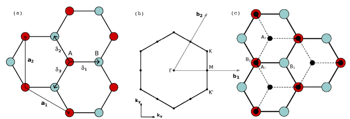
Both crystals have two dimensional hexagonal structure shown in Fig. 1 (a). A unit cell contains two sites, one of type A and the second one of type B. The linear combinations of lattice vectors:
| (1) |
generate only A sites while sites in B sublattice are generated by , where has to be choosen as one of the three nearest neighbours vectors:
| (2) |
The quantity stands for a lattice constant. The corresponding Brillouin zone (see Fig. 1 (b)) is a hexagon in reciprocal space with basis vectors given by:
| (3) |
Two inequivalent corners of the Brillouin zone and can be chosen as follows:
| (4) |
Although there is a slight difference between lattice constants of graphene and hexagonal boron nitride, we take the same value for both materials.hbn
We present a simple model of graphene on hexagonal boron nitride in Fig. 1 (c). The top layer consists of carbon atoms, while the bottom layer is a hexagonal boron nitride sheet. As indicated in Ref. hbn, , it is the lowest energy orientation of the graphene layer with respect to the h-BN with the equilibrium distance between the sheets Å. A two dimensional Brillouin zone is shown in Fig. 1 (b). One can regain the AB stacked bilayer graphene replacing boron and nitrogen by carbon atoms and substituting interlayer distance by Å.
Due to hybrydization the resulted three bonds are located in the graphene plane while two overlapping orbitals form bond perpendicular to the sheet. Therefore and orbitals can be analyzed independently. We restrict our considerations only to energy bands because they are responsible for unique properties of graphene. Two Bloch functions, constructed from atomic orbitals for two inequivalent carbon atoms A and B, provide the basis functions for single layer graphene. For bilayer system we assume a basis as orbitals of respective atoms with Bloch factors:
| (5a) | |||
| (5b) | |||
| (5c) | |||
| (5d) | |||
where , and , are the positions of inequivalent atoms in the first and second layer, while , and , are orbitals in respective atoms. We use atomic valence orbitals and orbitals with close values of energieskolos (5) to construct the eigenfunctions:
| (6) |
According to the procedure given in Ref. nanotubes, we introduce the following quantities representing the energies of electrons of level in the crystal:
| (7a) | |||
| (7b) | |||
and in-plane and an out-of-plane hopping parameters:
| (8) |
| (9) |
| (10) |
where is a hamiltonian of the system, and only the nearest neighbours interactions are assumed in the system. We construct then a hamiltonian in the basis (5):
| (11) |
with
| (12) |
and we define the overlapping matrix in the form:
| (13) |
where , and denote overlapping integrals which are assumed to be small. In fact, since we study the band structures in the vicinity of the Brillouin zone corners, we can neglect all of them.partoens4
The eigenvalue problem is simple in case of monolayer system and we start with providing a short outline of the obtained results.
II.1 Graphene and boron nitride monolayers - an outline
In case of graphene monolayer the hamiltonian (11) reduces to right bottom block with the orbital energies of the level in carbon lattice . We have the solutions:
| (14) |
where signs define two branches of the energy dispersion curves and , are called bonding and antibonding energy bands, respectively. It is seen from definition (12) that at the and points it holds:
| (15) |
and a zero band gap is easily recognized. It means that the electrons in two sublattices do not interfere if they are at the Brillouin zone corners and it is a direct consequence of the symmetry of the system. It is worthwhile to remind that this does not change if hopping between non nearest neighbours is included in the model.
The hamiltonian (11) reduces to left top block for the case of boron nitride monolayer. The solutions can be written in a simple form:
| (16) |
with
| (17) |
defining the band gap at point. Then, in the corners of the Brillouin zone we have:
| (18) |
In this case the symmetry between A and B sublattices is broken because the energies of the onsite atoms are not the same representing boron and nitrogen, respectively. The band structure is similar, but at the () point a gap with the magnitude opens. In the first approximation, it emerges that energies and could be taken close to energies of N and B states in respective atoms. However, for such choice, the value of would be about 0.2 eV while in the boron nitride a wider energy gap (5.9 eV) is observed.
This considerable separation between valence and conduction bands is explained by difference in electronegativities of boron and nitrogen which is responsible for a negative charge transfer in the direction of nitrogen. Then the covalent bond gains partially ionic character which produces a Madelung energy. By means of DFT calculations it has been found that for a freestanding h-BN sheet about 0.56 electrons are transferred from B to N.blaha This yields a sizable Madelung contribution to the lattice stability of 2.4 eV per 1x1 unit cell. The distinguishability of boron and nitrogen leads to the insulator behaviour. The valence band is mainly constituted by the nitrogen sublattice while the conduction band by the boron sublattice. This property is reflected in a density of states obtained by the ab initio calculations.turcy
II.2 Bilayer graphene versus graphene on hexagonal boron nitride
A secular problem for bilayer systems leads to a quartic equation, which can be solved by radicals. For given parameters one can provide the solutions explicitly as a function of . At and points the condition (15) holds, thus we can express the eigenvalues of (11) for arbitrary parameters:
| (19) |
| (20) |
| (21) |
| (22) |
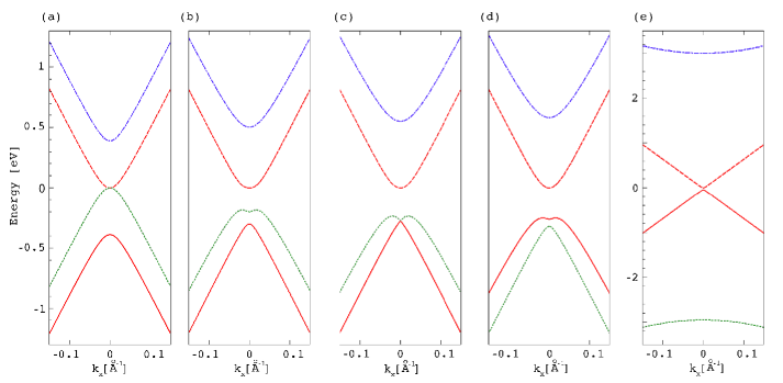
In Fig. 2 we plot the band structures of the system described by the general hamiltonian (11) for various choices of (7) and fixed hopping parameters. For simplicity we assume and . We start with the freestanding BLG (Fig. 2 (a), ). A difference between onsite energies (Fig. 2 (b)) generates the ’Mexican hat’ structure in the valence band which is also observed in bilayer graphene with substrate induced asymmetry.mucha Further increasing of the asymmetry value leads to the touching of two valence bands at the and points (Fig. 2 (c)). For the values of larger than (Fig. 2 (d)) the bands assigned to the eigenvalues and change their order, thus in the limit of graphene on h-BN a lower valence band gains N character (Fig. 2 (e)).
The band structure of graphene/h-BN system presented in Fig. 2 (e) has been obtained for the values of chosen to assure a proper energy gap for the case of h-BN monolayer described in the previous section. In consequence, a gap between valence and conduction bands is about 50 meV which is of the same order as the one obtained from DFT calculations for graphene on four layers of h-BN substrate.hbn In the vicinity of the Brillouin zone corners the band structure possesses nearly carbon character indicating a weak interaction between the layers.
In the present considerations, we have shown that evolution from BLG towards the graphene on h-BN system is related to changes of the onsite asymmetry in the bottom layer.
II.3 Bilayer system in an external electric field
The electronic properties of a graphene bilayer in the presence of an external electric field applied perpendicularly to the system have been widely studied.mccann ; biased We are interested here in the properties of bilayer system consisting of graphene and h-BN monolayers. The external perpendicular field gives rise to an electrostatic energy difference between these two layers which is parametrized by . The interlayer asymmetry induced by an external field in the bilayer system shown in Fig. 1 (c) can be described by the hamiltonianbiased in the tight binding approximation:
| (23) |
When the condition (15) holds, one can receive the eigenvalues for arbitrary parameters:
| (24) |
| (25) |
| (26) |
| (27) |
where we have assumed, for simplicity, .
As a starting point to study the influence of the electric field on the band structure we find the values of parameters for which two bands touches in the () point. A simple analysis shows that it occurs in three cases. First one gives the value of when the bands corresponding to and are joined:
| (28) |
second one when the bands corresponding to and meet in K point:
| (29) |
and the third one comes from the condition =:
| (30) |
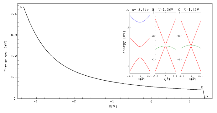
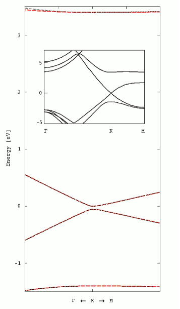
Figure 3 shows the changes of a band gap as a function of while the insets present the band structure around the point in three cases described by conditions (28), (29), (30) and indicated by letters A, B and C on the plot. Since the condition (28) gives an imaginary value of , the band structure in point A on the curve can be considered only by taking its real part. Inset A in Fig. 3 depicts the band structure determined for and it follows that it is the lowest value of the voltage, for which a direct band gap is observed. It achieves a value of . The second condition (29) predicts that two valence bands touches, which is shown in inset B of Fig. 3. Finally, condition (30) leads to the situation when the valence and conduction bands meet in the corner of the Brillouin zone (inset C in Fig. 3). Moreover, in the last case we observe a large slope of conduction band in the vicinity of point which indicates that nearly conical touching can be recognized ().
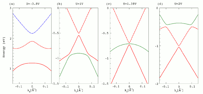
In Fig. 4 we present the band structures for the values of voltages chosen in the way to show what happen in the regions outside the boundaries determined by and and in the regions between points A - B and B - C (see Fig. 3). For the values of voltages lower than (Fig. 4 (a)) and higher than (Fig. 4 (d)) the band gap is indirect which is not observed in case of the bilayer graphene when valence and conduction bands have the same Mexican hat shape. Moreover, for higher positive voltage (Fig. 4 (d)) we observe the restructuring of conduction band which seems to be a result of an anticrossing interaction between highly localized states of electronegative nitrogen atoms with the extended conduction band states of graphene.walukiewiczunp The electronic states loose their localized character and form band through an interaction with extended states. For the voltages from A - B range of values (Fig. 4 (b)), we observe an upward movement of the valence bands edges. It can be interpreted as induced by hybridization of the carbon states comprising the higher valence band with the close lying localized states of N. This bands anticrossing phenomenon leads to the shift of the valence bands edges and to the reduction of the band gap.walukiewiczprb
It is worthwhile to notice that the band structure modifications of the bilayer graphene/h-BN system induced by the external electric field is similar to the behaviour of the band structure in mismatched III-N-V and III-V semiconductor alloys.walukiewiczprb ; walukiewiczprl ; walukiewiczsol
III Density functional calculations
We have performed density functional calculations for bilayer graphene/h-BN system using PWscf packagepwscf of the Quantum Espresso distributionqe . A plane wave expansion with an energy cutoff at 400 Ry and the Perdew-Zunger LDA exchange - correlation functionalperdewzunger were used. Core electrons were described by norm conserving pseudopotentials. The Brillouin zone was sampled on a uniform 36 36 1 grid with the tetrahedron methodtetrahedron . The interactions with spurious replicas along the z direction were avoided by setting a large size of a supercell Å. We have taken a value of lattice constant a=2.456 Å. Total energies were convergent to Ry.
| 2.64 | 2.79 | 0.43 | 3.34 | -1.40 |
We fit the TB band structure with DFT data to test the model analyzed in Sec. II B. The fitting procedure has been applied to the points taken from the straight vicinity of K point along line using the least squares method. We present the calculated DFT and TB band structures in Fig. 5. It is easy to see, that both electronic structures are well fitted. The small discrepancies start to appear only at the higher conduction band. The obtained values of TB parameters are listed in Table 1.
As it is expected, in local density approximation (LDA), the difference between boron nitride bands is underestimated. Its value should be higher than 5.9 eVgwhbn , while the currently determined value is in the order of 4.7 eV which is in a good agreement with LDA results for pure boron nitride honeycombturcy .
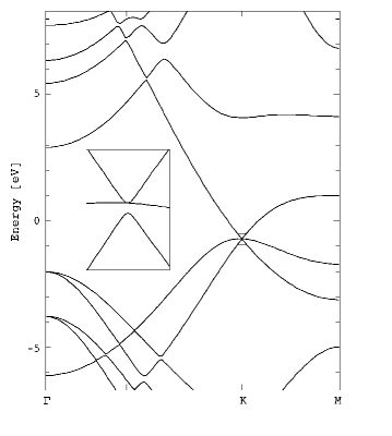
In the second stage, we have performed the ab initio calculations for graphene/h-BN system in the presence of a constant electric field simulated by a sawlike potential. The results confirm TB predictions related to the band structure modifications described in Sec. II c. It should be noticed that similarly to the case of bilayer graphenehongkimin ; gava we observe screening effects. It means that in order to obtain expected shift and deformation of bands we have to apply an electric field higher than estimated in TB model. Figure 6 presents DFT band structure for the case given in inset C of Fig. 3. The TB predicted value of is too low to reproduce the gap closing, in fact we have to apply V.
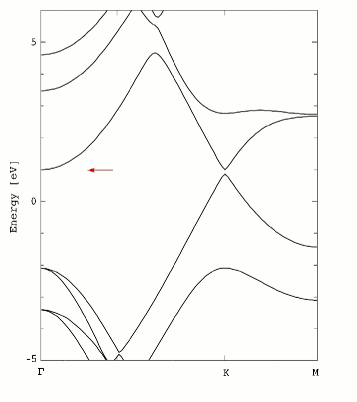
In Fig. 7 we show the band structure of the graphene on h-BN in the presence of an electric field parametrized by negative U of the effective value equal to -2 V. We can observe a direct gap of over 127 meV between valence and conduction band. One can notice, however, that at the point one of the boron nitride originating bands starts to coincide with the energy level of the bottom edge of carbon conduction band (at the K point), which leads to an indirect band gap of the system. For the higher absolute values of potential difference, a band gap decreases due to the presence of unwanted edge and achieves negative values typical for semimetals. When a system gains semimetallic character, very strong screening effects prevent further increase of the effective voltage.
IV Final remarks
We have studied the electronic properties of a graphene/h-BN bilayer system using the minimal tight binding model. Particular attention has been given to the presence of external electric field perpendicular to the bilayer system which gives rise to a finite gap in the spectrum, whose opening and width are controlled by the applied voltage. The use of TB approach allows to show that graphene/h-BN system and bilayer graphene are very closely related.
Moreover, we propose a very simple model as a starting point for similar considerations of more sophisticated substrates and interactions with metallic contacts.holendrzy ; klusek Further generalization on a larger number of AB stacked layers of graphene and AA stacked h-BN sheets can also be made.
We have shown that the band structure may be modified and tuned to meet specific requirements for potential logic devices. We report the energy gap tuning in the range starting from 0 to about 130 meV and effective masses in conduction band varying from to , which are smaller than Dirac fermions’ masses in bilayer graphene. One can easily predict that additional quasi-particle interactions included in calculations, for instance within a GW scheme, will indicate an increased value of the gap.hbn Moreover, DFT as a ground-state theory does not give a proper description of excited states. Therefore, it is possible that an energy of bottom edge of the conduction band (see Fig. 7) is not correctly determined. On the other hand, if one could engineer the band structure to shift or deform this conduction band edge then the voltage induced band gap could be as large as predicted by TB calculations (over 430 meV see Fig. 4 (a)).
Since a significant step towards the bilayer graphene FET production has been recently taken,nanoletters it has to be stressed that various modified bilayer systems could play a crucial role in the future nanoelectronics. Recent studies on transferring exfoliated graphene onto arbitrary substratesnakladanie suggest that the fabrication of graphene on h-BN could be now realized.
Acknowledgements.
We are grateful to Piotr Kosiński for helpful discussions and to Igor Własny for careful reading. This work is financially supported by Polish Ministry of Science and Higher Education in the frame of grant ”Investigations of electronic structure of graphene deposited on conductive and nonconductive surfaces by STM/STS/CITS/AFM and quantum electrodynamics N N202 204737”. One of us (J.S.) acknowledges support of the European Social Fund and Budget of State implemented under the Integrated Regional Operational Program, Project: Scholarship supporting postgraduate students’ innovative scientific research. Figure 1 was prepared using the XCrysDen program.kokalj*
References
- (1) K. S. Novoselov, A. K. Geim, S. V. Morozov, D. Jiang, Y. Zhang, S. V. Dubonos, I. V. Grigorieva, and A. A. Firsov, Science 306, 666 (2004)
- (2) A. H. C. Neto, F. Guinea, N. M. R. Peres, K. S. Novoselov, and A. K. Geim, Rev. Mod. Phys. 81, 109 (2009)
- (3) M. C. Lemme, Solid State Phenomena 156-158, 499 (2010)
- (4) F. Xia, D. B. Farmer, Y.-m. Lin, and P. Avouris, Nano Letters (2010), http://dx.doi.org/10.1021/nl9039636
- (5) X. Li, X. Wang, L. Zhang, S. Lee, and H. Dai, Science 319, 1229 (2008)
- (6) X. Wang, Y. Ouyang, X. Li, H. Wang, J. Guo, and H. Dai, Phys. Rev. Lett. 100, 206803 (2008)
- (7) J. Nilsson, A. H. C. Neto, F. Guinea, and N. M. R. Peres, Phys. Rev. B 78, 045405 (2008)
- (8) E. McCann, Phys. Rev. B 74, 161403 (2006)
- (9) E. V. Castro, K. S. Novoselov, S. V. Morozov, N. M. R. Peres, J. M. B. L. dos Santos, J. Nilsson, F. Guinea, A. K. Geim, and A. H. C. Neto(2008), arXiv:0807.3348
- (10) T. Ohta, A. Bostwick, T. Seyller, K. Horn, and E. Rotenberg, Science 313, 951 (2006)
- (11) J. Kedzierski, P.-L. Hsu, P. Healey, P. Wyatt, C. Keast, M. Sprinkle, C. Berger, and W. de Heer, IEEE /Transactions on Electron Devices 55, 2078 (2008)
- (12) J. B. Oostinga, H. B.Heersche, X. Liu, A. F. Morpurgo, and L. M. Vandersypen, Nat. Mater. 7, 151 (2008)
- (13) E. V. Castro, K. S. Novoselov, S. V. Morozov, N. M. R. Peres, J. M. B. L. dos Santos, J. Nilsson, F. Guinea, A. K. Geim, and A. H. C. Neto, Phys. Rev. Lett. 99, 216802 (2007)
- (14) Y. Zhang, T.-T. Tang, C. Girit, Z. Hao, M. C. Martin, A. Zettl, M. F. Crommie, Y. R. Shen, and F. Wang, Nature 459, 820 (2009)
- (15) K. F. Mak, C. H. Lui, J. Shan, and T. F. Heinz, Phys. Rev. Lett. 102, 256405 (Jun 2009)
- (16) H. Min, B. Sahu, S. K. Banerjee, and A. H. MacDonald, Phys. Rev. B 75, 155115 (2007)
- (17) E. V. Castro, N. M. R. Peres, J. M. B. L. dos Santos, F. Guinea, and A. H. C. Neto, Journal of Physics: Conference Series 129, 012002 (2008)
- (18) L. Liu and Z. Shen, Appl. Phys. Lett. 95, 252104 (2009)
- (19) G. Giovannetti, P. A. Khomyakov, G. Brocks, P. J. Kelly, and J. van den Brink, Phys. Rev. B 76, 073103 (2007)
- (20) T. Greber, in Handbook of Nanophysics, Graphene and Boron Nitride Single Layers (Taylor and Francis Books, 2010)
- (21) G. W. Semenoff, Phys. Rev. Lett. 53, 2449 (1984)
- (22) P. R. Wallace, Phys. Rev. 71, 622 (1947)
- (23) B. Partoens and F. M. Peeters, Phys. Rev. B 74, 075404 (2006)
- (24) A. A. Avetisyan, B. Partoens, and F. M. Peeters, Phys. Rev. B 79, 035421 (2009)
- (25) A. A. Avetisyan, B. Partoens, and F. M. Peeters, Phys. Rev. B 80, 195401 (2009)
- (26) J.-C. Charlier, X. Gonze, and J.-P. Michenaud, Phys. Rev. B 43, 4579 (1991)
- (27) A. Grüneis, C. Attaccalite, L. Wirtz, H. Shiozawa, R. Saito, T. Pichler, and A. Rubio, Phys. Rev. B 78, 205425 (2008)
- (28) W. Kołos, Chemia kwantowa (PWN, Warszawa, 1978)
- (29) R. Saito, G. Dresselhaus, and M. S. Dresselhaus, Physical Properties of Carbon Nanotubes (Imperial, London, 1998)
- (30) M. S. Dresselhaus and G. Dresselhaus, Adv. Phys. 30, 139 (1981)
- (31) J. C. Slonczewski and P. R. Weiss, Phys. Rev. 109, 272 (1958)
- (32) J. W. McClure, Phys. Rev. 108, 612 (1957)
- (33) G. B. Grad, P. Blaha, K. Schwarz, W. Auwärter, and T. Greber, Phys. Rev. B 68, 085404 (2003)
- (34) M. Topsakal, E. Aktürk, and S. Ciraci, Phys. Rev. B 79, 115442 (2009)
- (35) M. Mucha-Kruczyński, O. Tsyplyatyev, A. Grishin, E. McCann, V. I. Fal’ko, A. Bostwick, and E. Rotenberg, Phys. Rev. B 77, 195403 (2008)
- (36) W. Walukiewicz, Lawrence Berkeley National Laboratory. LBNL Paper LBNL-51164. (2002), http://www.escholarship.org/uc/item/2vn3c6vs
- (37) K. Alberi, J. Wu, W. Walukiewicz, K. M. Yu, O. D. Dubon, S. P. Watkins, C. X. Wang, X. Liu, Y.-J. Cho, and J. Furdyna, Phys. Rev. B 75, 045203 (2007)
- (38) W. Shan, W. Walukiewicz, J. W. Ager, E. E. Haller, J. F. Geisz, D. J. Friedman, J. M. Olson, and S. R. Kurtz, Phys. Rev. Lett. 82, 1221 (1999)
- (39) K. Alberi, J. Wu, W. Walukiewicz, K. M. Yu, O. D. Dubon, S. P. Watkins, C. X. Wang, X. Liu, Y.-J. Cho, and J. K. Furdyna, Phys. Status Solidi C 4, 1711 (2007)
- (40) S. Baroni, A. D. Corso, S. de Gironcoli, and P. Giannozzi, “Pwscf and phonon: plane-wave pseudopotential codes,” (2005), http://www.pwscf.org/
- (41) P. Giannozzi et al., Journal of Physics: Condensed Matter 21, 395502 (2009), http://www.quantum-espresso.org
- (42) J. P. Perdew and A. Zunger, Phys. Rev. B 23, 5048 (1981)
- (43) P. E. Blöchl, O. Jepsen, and O. K. Andersen, Phys. Rev. B 49, 16223 (1994)
- (44) X. Blase, A. Rubio, S. G. Louie, and M. L. Cohen, Phys. Rev. B 51, 6868 (1995)
- (45) P. Gava, M. Lazzeri, A. M. Saitta, and F. Mauri, Phys. Rev. B 79, 165431 (2009)
- (46) P. A. Khomyakov, G. Giovannetti, P. C. Rusu, G. Brocks, J. van den Brink, and P. J. Kelly, Phys. Rev. B 79, 195425 (2009)
- (47) Z. Klusek, P. Dabrowski, P. Kowalczyk, W. Kozlowski, W. Olejniczak, P. Blake, M. Szybowicz, and T. Runka, Appl. Phys. Lett. 95, 113114 (2009)
- (48) J. D. Caldwell, T. J. Anderson, J. C. Culbertson, G. G. Jernigan, K. D. Hobart, F. J. Kub, M. J. Tadjer, J. L. Tedesco, J. K. Hite, M. A. Mastro, R. L. Myers-Ward, C. R. Eddy Jr, P. M. Campbell, and D. K. Gaskill, Nano Letters (2010), http://dx.doi.org/10.1021/nn901585p
- (49) A. Kokalj, Comput. Mater. Sci. 28, 155 (2003), http://www.xcrysden.org/