A single atom detector integrated on an atom chip: fabrication, characterization and application
Abstract
We describe a robust and reliable fluorescence detector for single atoms that is fully integrated into an atom chip. The detector allows spectrally and spatially selective detection of atoms, reaching a single atom detection efficiency of 66 %. It consists of a tapered lensed single-mode fiber for precise delivery of excitation light and a multi-mode fiber to collect the fluorescence. The fibers are mounted in lithographically defined holding structures on the atom chip. Neutral 87Rb atoms propagating freely in a magnetic guide are detected and the noise of their fluorescence emission is analyzed. The variance of the photon distribution allows to determine the number of detected photons / atom and from there the atom detection efficiency. The second order intensity correlation function of the fluorescence shows near-perfect photon anti-bunching and signs of damped Rabi-oscillations. With simple improvements one can boost the detection efficiency to 95 %.
pacs:
03.75.-b, 42.50.Lc, 42.81.-i, 07.60.Vg1 Introduction
Detecting single neutral atoms state selectively is one of the essential ingredients for developing quantum atom optics, atomic physics based quantum technologies and a prerequisite for many quantum information experiments.
The first single atom experiments relied on photo ionization for detection [1]. Nowadays single atom observation is usually performed optically using fluorescence or absorption detection. Cavity assisted detection schemes are predominant and very successful for absorption detection [2, 3, 4, 5, 6, 7, 8, 9, 10, 11], but require active stabilization, increasing the complexity and sensitivity to environmental disturbances.
Fluorescence detection of single atoms can be very efficient if the atom remains localized, since long integration times allow collecting many fluorescence photons. This is realized in single atom in a MOT [12], dipole traps [13] or trapped single ions [14, 15, 16]. Fluorescence detection of moving atoms which have a short, finite interaction time with the detector is significantly harder and requires both: supreme background suppression and a high collection efficiency to reach single atom sensitivity. For freely falling atoms high collection efficiencies have been achieved using a macroscopic mirror setup covering almost 4 [17]. Cavities can be used to enhance the fluorescence signal [9, 10, 18].
A powerful technique to experiment with ultra cold neutral atoms are atom chips [19] which employ micro-fabricated wires and electrodes to generate magnetic and electric fields for quantum manipulation of neutral atoms few micrometers above the chip surface [20, 21, 22]. Many components of integrated matter wave technology have been demonstrated including, combined magnetic/electrostatic traps [23], motors and shift registers [24], atomic beam splitters [25] the creation of Bose-Einstein condensation (BEC) [26, 27, 28], atom interference [29, 30], the the integration of optical lattices [31].
Recently it was demonstrated that atoms in magnetic guides [32] or on chips can be detected by field ionization near nano-structures [33, 34], by mounted optical fibers in absorption [35], in fluorescence [36], by using integrated waveguides [37], or with the help of cavities [8, 9, 11]. The latter require active alignment and are technologically very challenging. Miniaturizing the different, highly sophisticated and efficient optics detection methods benefits from scaling with size [38] and allows integration.
In this manuscript we describe in detail design, implementation and application of our very simple and robust integrated fluorescence detector [36] that reaches a single atom detection efficiency of and a high signal to noise ratio (SNR) of up to 100 without the need for either localization of the atoms or the assistance of a cavity. The miniaturized detector is based on optical fibers fully integrated on an atom chip [39, 40] using lithographically fabricated SU-8 mounting structures [41] and allows to examine the statistical distribution of the atoms in a magnetic guide as well as observing non-classical fluorescence emission of single atoms [42]. In the outlook we discuss a straight forward improvement of our present set-up that will allow us to build atom counters with close to unit efficiency fully integrated on the atom chip.
2 Basic design
A very simple way of detecting an atom is to observe its fluorescence. The basic idea is to drive a (closed) transition of the atom to an excited state with an external light field and to detect the spontaneously emitted photons. The sensitivity of the detection and its fidelity depend on the number of scattered photons, the detection efficiency of the scattered light and the suppression of background noise. A well designed fluorescence detector collects as much light as possible and simultaneously has a negligible background. In the ideal case a single detected photon implies that an atom is present in the detection region.
In principle, there is no fundamental limit to the efficiency of a fluorescence detector as long as the atom is not lost from the observation region. Long integration times allows the collecting of many fluorescence photons and efficient discrimination from background. Such a setting was realized for single ions in ion traps [14, 15, 16], for a single neutral atom in a dipole trap [13] or for counting neutral atoms in a magneto-optical trap [12]. Free neutral atoms are considerably harder to detect because the few scattered photons are difficult to distinguish from background light.
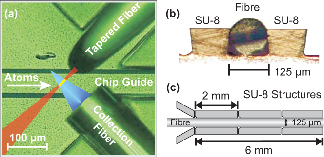
We achieve efficient light collection with small background by employing a fiber optics setup [36] as shown in figure 1(a). Our fluorescence detector is built using a single mode tapered lensed fiber which delivers the excitation light and a multi-mode fiber to collect the fluorescence. The multi-mode fiber is aligned at angle with respect to the tapered lensed fiber. If no atom is present in the beam focus, very little light is scattered into the fiber. As soon as an atom is present the multi-mode fiber collects the scattered photons.
Such an arrangement is very reminiscent of a confocal microscope. The excitation of the atoms is at a very small focal spot of the lensed fiber. The collection fiber collects light preferably from the region around the focal spot. Altogether such an arrangement leads to efficient light collection and superb reduction of background.
3 Implementation
For stable and reliable operation both the excitation and detection fibers should be fully integrated into the atom chip. External mountings are poor alternatives since they might move relative to the chip structures and hence lead to non-reproducible results. The fibers can be glued to the chip by first employing fiber grippers for positioning and alignment. While this method may result in good alignments it is cumbersome to employ and requires significant time and skill to achieve consistent results. Lithographically fabricated robust and precise fiber mounting structures [41] are a great help in assembling the detector.
3.1 Fabrication
Our atom chip holding the micro structures and the detector is fabricated on a m thick silicon substrate. Using optical lithography the micro structures to manipulate the atoms are patterned into an high quality evaporated gold layer [39, 40] of 2 m thickness. These wire micro structures support current densities exceeding A/cm2 without the risk of wire destruction.
To achieve the precise alignment of the fibers and robust integration on the atom chip we employ a lithographically patterned layer of SU-8 on top of the chip structures. SU-8 [43] is an epoxy based negative photo resist which is typically developed using UV-radiation in the range 365-436 nm. SU-8 has high mechanical, chemical and thermal stability. Its specific properties facilitate the production of thick structures with very smooth, nearly vertical sidewalls. With a single SU-8 layer a coating film thickness of up to 300 m is possible. Once fully developed its glass transition temperature is approximately C with a degradation threshold around C. Both temperatures are not reached during operation of the atom chip.
The detection fibers are held in SU-8 trenches 90 m deep and 125 m wide, corresponding to the fiber diameter. Careful selection of the fabrication parameters produces slightly undercut sidewalls, as shown in figure 1(b). The layer thickness of 90 m is chosen to be larger than the fiber radius, which allows the undercut to effectively clamp the fibers to the chip surface.
The total length of the trenches was chosen to be 6 mm, sectioned into three 2 mm long substructures to reduce mechanical stress during thermal expansion (figure 1(c)). The entry port is funneled to simplify the insertion of the fiber. The total length guarantees supreme pointing stability, while allowing accurate positioning of the fibers with longitudinal alignment precision of a few ten nanometers, as well as excellent long term stability. Temperature changes and gradients up to C resulted in no measurable misalignment of the fibers. Long term stability of more than three years under experimental conditions has been achieved.
In fabricating the fiber mounts a % shrinkage of the SU-8 during development has to be taken into account [43], leading to a slight variability in the dimensions of the holding structures. It should be noted here that the variations in fiber diameters are large in comparison. The diameter of a fiber used in the experiment is specified with a precision of only 1 m to a cladding diameter of m. Therefore we fabricated a set of 3 parallel mounting structures with slightly different sizes (124.5 m, 125 m and 125.5 m).
To assess the quality and stability of the alignment structures and the glued fibers, we used the SU-8 structures to hold fiber optical resonators [44]. The finesse of the resonator strongly depends on losses introduced by misalignment. In our tests we measured a very small additional average loss in the spliced and mounted resonators of % which, neglecting other additional losses, corresponds to a maximal transversal misalignment of less than nm.

3.2 Integration in the experiment
With a diameter of the mounted fibers of 125 m, the detection region is situated 62.5 m above the chip surface. To avoid stray light from the mounting structures when loading the atoms in the mirror MOT, the detector is built 5.5 mm away from the chip center. A magnetic guide on the chip transports the atoms to the detector (see figure 2).
The fibers mounted on the atom chip are then connected to the outside of the vacuum chamber via an ultra-high vacuum (UHV) compatible feed-through [45]. The whole setup can be baked to C and achieves UHV below mbar.
3.3 Excitation of the atoms
To excite the atoms to fluorescence the tapered lensed fiber delivers the light to a focal spot in the guide potential minimum. Our tapered fibers feature a focal length of with a focal diameter of m. For the F=2F’=3 transition in saturation intensity is reached in the focus at a power of pW. The focus of the tapered fiber defines the interaction region as shown in figure 1(a) and is located m (half a fiber diameter) above the chip surface.
The excitation light is generated by an external cavity diode laser (ECDL) frequency stabilized to the F=2F’=3 transition with a precision better than 1 MHz, smaller than the natural line width of the transition. The probe laser is frequency stabilized to a reference laser by means of a frequency offset (beating) lock. This locking scheme enables us to shift the lock point by several hundred MHz during operation, allowing to probe the atomic ensemble over the full range of the Rb-D2 transition.
For additional intensity stabilization part of the light is split off in a commercial fiber beam splitter and directed to a PIN-type photo diode (PD) (see figure 2(b)). The PD signal is fed into custom built proportional-integral-differential lock electronics (PID) stabilizing the beam power with an uncertainty below 10 pW to the set value by controlling the output level of an acousto-optical modulator (AOM) used as a fast light switch. The polarization of the excitation light can be rotated employing mechanical fiber paddles.
Using a mechanical fiber splice the stabilized excitation light is coupled into the single-mode tapered lensed fiber guiding the light into the vacuum chamber to the detection region.
3.4 Light Collection
The light scattered by the atoms is collected by a multi-mode fiber that guides the light to a single photon counting module (SPCM). To protect the SPCM and to filter non-resonant background light a narrow interference filter is included in the beam path (3 nm FWHM).
The multi-mode fiber has a limited field of view, given by its numerical aperture of NA and the core diameter of m. Only light hitting the core at angles up to maximally will be collected. Consequently only emission from atoms within the dark blue cone marked in figure 1(a) is collected with the full NA. Hence the region of maximum collection efficiency for the atomic signal is given by the intersection of the excitation mode field (red) and the full NA cone. This defines the detection region, which is depicted yellow in figure 1(a).
The height of the detection region is automatically aligned to the excitation region since the outer diameters of the fibers match. By aligning the MM fiber such that the collection cone defined by the numerical aperture overlaps with the excitation region we reach both a highly selective excitation of the atoms and a matched collection region. The angle between the tapered (excitation) and the multi-mode (detection) fiber has been chosen to be . This leads to an excellent geometrical suppression of stray light. Of each nano watt of excitation light only about 30 photons per second are collected by the detection fiber, corresponding to a stray light suppression of better than . The detection setup has been positioned such that both fibers are at to the guide to avoid blocking of the guide.
For our collection fiber (NA=0.275) a maximum photon collection efficiency of % can be determined. Together with the finite efficiency of the SPCM and optical losses this leads to a total photon detection efficiency of .
3.5 Experimental Cycle
In our experiments the atom chip [19, 20] serves as the experimental platform for efficient cooling and trapping of the atoms and for transporting them in a magnetic guide to the detection region.
Our experimental procedure is described in [46]. The heart of our setup is a hybrid macroscopic-microscopic atom chip assembly. It holds the macroscopic wire structures used to pre-cool and capture the atoms in the primary phase of the experiment as well as the appropriately designed wire micro structures on the atom chip needed for trapping and manipulating the atoms, including the atom detector.
The experimental procedure starts typically with more than 87Rb atoms accumulated in a mirror MOT. The atoms are subsequently optically pumped into the state and transferred to a Ioffe-Pritchard type magnetic trap on the atom chip generated by a Z-shaped wire on the chip surface. The procedure is optimized by a genetic algorithm [47]. The atoms in the magnetic trap are released into a magnetic guide (L-shaped wire) where the atomic cloud can expand toward the detector. The position of the magnetic guide above the chip surface is aligned with the focus of the tapered lensed fiber at the detection region by adjusting the current through the chip wire and the strength of the external magnetic field [20].
When the atoms are released from the initial Z trap into the magnetic guide they thermally expand towards the detector. In the focus of the lensed fiber the atoms are excited by a laser operating near one of the the rubidium D2 transitions (for example tuned to the to transition) and the fluorescence photons are collected by the multi-mode fiber and detected by a single photon counting module (SPCM), their arrival times are recorded with 1 ns resolution. The experiment is repeated several times to measure the photon statistics. A typical signal is shown in Fig. 3a.
In the current experiment the phase space density in the magnetic trap and guide is always less than .
4 Characterization of the atom detector
One observation in our experiments is that we see the full length of the atom pulse guided in the magnetic guide (Fig. 3(a)) even though the resonant excitation light of the detector is always on. These measurements show that in our experiments effects of stray excitation light on the guided atoms can be neglected. This is quite remarkable since magnetic traps are extremely sensitive to light scattering. On average, scattering of a little more than a single photon is sufficient to pump the atom into a magnetically un-trapped state, removing it from the magnetic guide.
Figure 3(a) shows the atomic signal together with its variance, calculated from 600 consecutive measurements. The shape can be described by a 1D Maxwell-Boltzmann distribution given by the temperature of the atoms when the reflection of the part of the atom cloud that starts to expands towards the closed end of the guide is also taken into account. The measured temperature of agrees with independent measurements via time of flight methods.
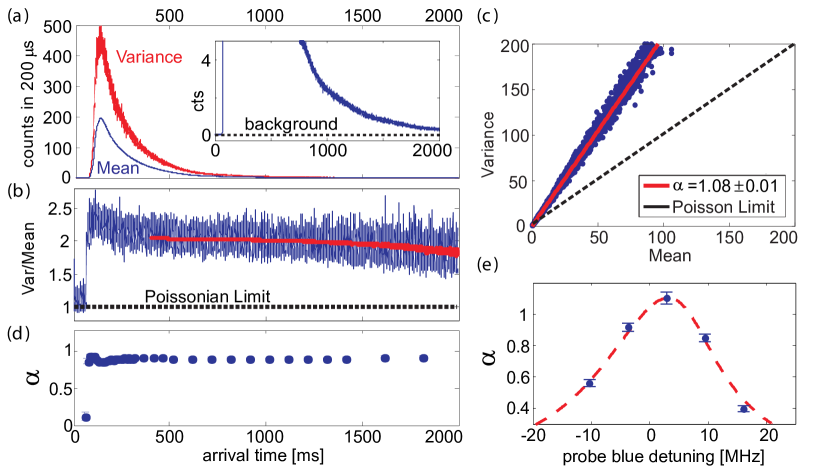
(a) Mean and variance of the photon counts: The lower (blue) curve shows the mean photon count for 600 experimental runs while the upper (red) curve shows their variance . An integration time of has been used. Inset: Even after 2 s the signal is still significantly above the background level of 0.06.
(b) Ratio /: As soon as the atoms arrive, / exhibits a sudden jump to a super-poissonian value of . Even though remains constant, the ratio decreases with atomic density as background becomes more important. The red line gives a fit according to equation 1 over more than two orders of magnitude in atom density. Note that the initial overshoot is an artifact of the analysis because around peak the steep sloes can not be neglected during the 200 s integration time.
(c) as a function of the mean recorded count rate . An analysis according to equation 1 (red line) yields a signal strength of counts per atom (integration time s). The dashed line corresponds to Poissonian statistics.
(d) The signal strength remains constant and is independent of atom density over three orders of magnitude. Here is evaluated for a shorter s and shows a reduced value of (compare figure 4).
(e) as function of the probe beam detuning reveals an optimal blue detuning of 3 MHz. The dashed red line is a model based on ref.[17].
4.1 Background
The fiber-based detector presented here has exceptionally low background count rate of only counts per seconds (cps) at 1nW resonant probe light . The dominating contribution are the dark counts ( cps) of the employed photon counter (Perkin-Elmer, SPCM-AQR-12).
Despite the proximity of the atom chip surface (at a distance of 62.5 m) the influence of stray probe-light is essentially eliminated with a suppression of better than . 1 nW excitation light contributes only cps to the background.
This excellent suppression of stray light is achieved by the fact that the a tapered lensed fiber delivers excitation light efficiently to a very small detection region and the multi-mode fiber, mounted at an angle of 90 degree, selectively collects the fluorescent photons from this small volume (Fig. 1a). Basically all the background light originating from scattering on the close by chip surface or the vacuum chamber is blocked very efficiently, because it is not matched to the guided modes in the collection fiber. In this sense the setup has characteristics similar to a confocal microscope, with the difference that the involved point spread functions are different.
Other background sources are stray light from the outside and the glow of the hot dispensers. An interference filter efficiently suppresses this remaining background to below 10 cps. (see Fig. 2b)
The excellent stray light suppression and overall small background level allows high fidelity detection of a single atom and accurate measurements of photon and atom statistics.
4.2 Signal Strength
An important parameter of the detector is the total number of photons that can be scattered by the guided atoms before they are lost for the detection process. We discuss this here for detecting atoms in F=2 using the F=2F’=3 transition. The total number of scattered photons can be estimated from the ratio of the fluorescence counts when exciting on the closed F=2F’=3 transition to the fluorescence counts on the open transition F=2F’=1. Exciting on the later an atom scatters slightly more than one photon before being optically pumped into the other hyperfine ground state, where it remains dark. We find that that in our detector each atom scatters photons when excited on the F=2F’=3 transition.
Combining this number with the overall photon detection efficiency % given above, we estimate that our detector sees in average photon from each atom passing by. This number was confirmed from independent global atom number measurements using absorption imaging.
The maximum signal per atom is generated not for resonant illumination, as might be expected, but for a blue detuning of 3 MHz of the exciting light field as shown in figure 3(e). Looking more into the details, the atoms accumulate a time dependent detuning during interaction with the probe field due to photon recoil induced Doppler shift. An initial blue detuning allows pushing the atoms trough resonance to maximize the total number of scattered photons during interaction [17].
4.3 Photon statistics
When an atom arrives at the detector, it absorbs and then re-emits photons. A few of these photons are counted by the SPCM. This photon scattering strongly disturbs the atom. Besides the photon recoil it will pump the atom into an un-trapped state and eventually into a different hyper fine ground state which is not excited by the probing light. Consequently after a time the atom will either leave the detection region and / or stop scattering photons. During detection each atom emits a photon burst, and on average photons are detected per atom. These photon bursts lead to a super-poissonian statistics for the detected photons (Fig. 3(b)). As we will show below we can relate the variance and the mean of the photon counts directly to the average number of photons detected per atom ().
A coherent light source of constant mean photon number creates a Poisson distributed photon stream with variance equal to the mean, and hence
The superpoissonian photon statistics for the atom detection events can be seen in Fig. 3(b) by the jump of / 1 as soon as atoms reach the detector. The statistical atom number fluctuations lead to increase in the photon noise. The atom number follows its own statistical distribution around a mean value and Mandel’s formula [48] can be used to describe the photon count distribution in the presence of atoms. The probability to measure counts is then expressed by folding the conditional probability
to measure counts in the presence of atoms with the atom number probability distribution .
The ratio / can then be calculated to
| (1) |
Hence the ratio of the variance of the photon counts to its mean value deviates from the Poissonian value 1 by the number of photon counts per atom times the ratio of variance to mean of the atom number.
If in addition a Poissonian background with is taken into account equation 1 is modified and the photon statistics can be expressed as
| (2) |
It is worth noting that this relation is independent of the actual atom number. For a Poissonian atom number distribution, i.e. , the signal strength can be measured as the slope of the relation variance versus mean (see figure 3(c)). Conversely, if is known equation 2 allows examining the statistical distribution of the atoms by measuring the photon count distribution. Figures 3(b) and (c) show the measured ratio / respectively versus together with a fit according to equation 2. The signal strength is determined to counts per atom (cpa), independent of atomic density over three orders of magnitude as demonstrated in figure 3(d).
A detailed analysis of the distributions show that an integration time of is needed to collect the full signal. Specific applications will benefit from shorter integration times. Figure 4(a) illustrates that drops rather slowly when reducing the integration time, while the mean number of background counts is a linear function of . For the integrated signal is cpa and even for we still find cpa.
4.4 Single atom detection efficiency
| [cpa] | SNR | |||
|---|---|---|---|---|
If we require to count at least one photon to see an atom the single atom detection efficiency is given by
In our experiment we find for s integration time. Background counts during this time lead to a false positive detection probability of . The relation between detection efficiency and integration time is shown in figure 4(b) together with the false positive detection probability for the current setup and a background reduced setup. While the detection efficiency is determined by the finite NA of the collection fiber the SNR is mainly limited by the background. Exchanging the SPCM by a low noise model with a dark count rate below 25 cps, a total background as low as 55 cps can be reached.
At the atom detection efficiency is with a false detection probability of only (see table 1). Defining a signal to noise ratio is reached in the current setup at (). At a background level of 55 cps will already be reached at ().
4.5 State Selectivity
A key signature of an ideal atom detector is the selectivity to internal states, distinguishing between the two hyperfine ground states is most important. Most atoms used in ultra-cold atom experiments have a sizable hyperfine splitting in the ground state, and consequently the two ground states can very easily be distinguished by (near) resonant fluorescence excitation, and state selectivity comes natural.
One characteristic of our fluorescence detector is that for high detection efficiency many scattered photons per atom are necessary, and consequently one needs to use a closed atomic transition. In our present experiment we use atoms with the two hyperfine ground states (F=1 and F=2 separated by 6.8 GHz). From the F=2 ground state there is a closed transition (F=2F’=3) where one can scatter 1000 photons before changing the hyperfine ground state by off-resonant excitation.
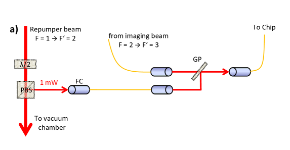
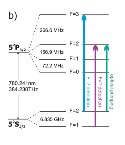
For atoms in the F=1 ground state the situation is not so simple. To ensure a high scattering rate excitation with F=1F’=2 transition is advantageous. This transition leads to rapid optical pumping into the other hyperfine ground state F=2, and light scattering stops. This can be overcome by adding a second laser excitation light tuned to F=2F’=3. With both lasers on one can scatter many photons also off atoms in the F=1 hyperfine ground state and detect them. For large intensities ( 300 pW) of light resonant with the F=1F’=2 transition, the value of signal strength has been measured to be comparable to the case of atoms in the F=2 ground state. The results of our measurements are summarized in table 2.
| Detector F=1 | Detector F=2 | |
|---|---|---|
| Atoms F=1 | ||
| Atoms F=2 |
Introducing the re-pumping laser means that a detector that detects F=1 will also detect F=2. For state selective detection this is not so much of a problem, because one can arrange two detectors in such a way that the first detector measures the F=2 atoms. This detector removes the F=2 atoms from the guide, but leaves the F=1 atoms propagating. A second detector behind the F=2 detector with both excitation frequencies will register the remaining atoms, all in F=1.
5 Measurements
We have employed our detector in a series of experiments to illustrate its robustness and versatility.
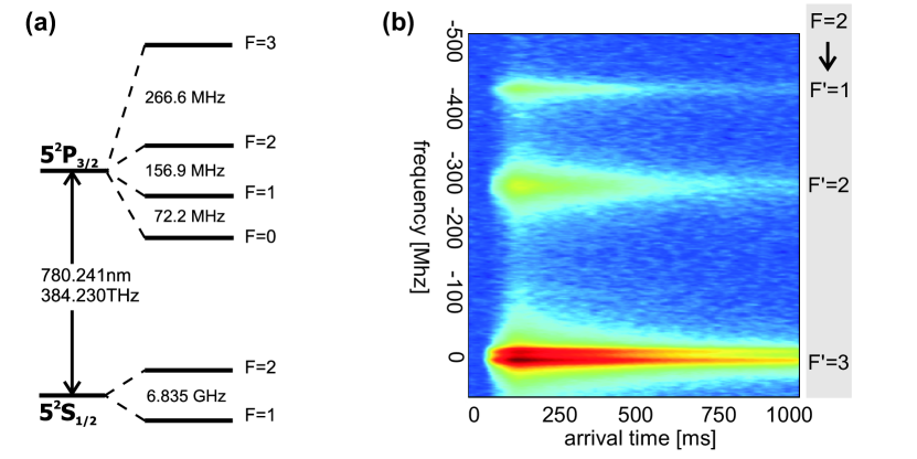
5.1 Spectroscopy in the magnetic guide
To demonstrate that the integrated fluorescence detector allows selective addressing of atomic levels we have measured the signal of an atom pulse passing the detector for different frequencies of the probe light.
For these measurements the atoms are prepared such that upon arrival at the detector the atoms are in the ground state and can be excited to the or state. Figure 6 displays the results of a 600 MHz sweep, starting 60 MHz blue detuned of the transition and going down to more than 100 MHz red detuning of the transition. The transition F=2F’=31, gives the strongest signal as expected and has correspondingly been employed for the high efficiency atom detection presented in the remaining sections of this paper. The F=2F’=1 transition gives the weakest signal, an atom scatters slightly more than one photon before being optically pumped into the other hyperfine ground state, where it remains dark. As discussed above the ratio between the signal observed for the F=2F’=X and F=2F’=1 transitions can be used to estimate how many photons the atom scatters at the F=2F’=X transition. In an optimized setting we observe that the 87Rb atoms scatter about 120 photons on the F=2F’=3 transition before they leave the detector.
For the measurement displayed in figure 6b a remaining magnetic field at the guide minimum of approximately 4 G was chosen. This field leads to a Zeeman-splitting of the magnetic sublevels. The splitting between adjacent levels is smaller than the line width for the and transitions, hence only one peak is observed. Note though, that for the transition the two cyclic transitions and can be clearly separated. The clear detection signal at the untrapped transition demonstrates that the scattering process is much faster than the dynamics of atoms leaving the trap.
5.2 Atom cloud extension in the guide
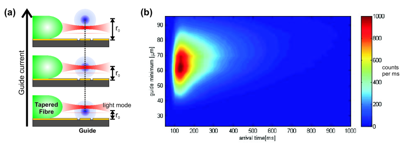
The position of the magnetic guide above the chip surface can be aligned relative to the focus of the tapered lensed fiber at the detection region by adjusting the current through the chip wire and the strength of the external magnetic field perpendicular to the wire. The guide is located at height , where is the vacuum permeability. Scanning the chip current at constant bias field, different slices through the guide potential can be probed, allowing to examine the extension of the atomic cloud in the guide with only small changes to the potential shape as shown in figure 7(a). Figure 7(b) shows the result of a scan shifting the guide potential minimum from 25 m to 95 m. The maximum signal is retrieved if the guide minimum is aligned with the detection area, given by the 5 m focal spot of the tapered lensed fiber and only the longitudinally fast atoms reach the outlying regions of the guide.
5.3 Time interval analysis
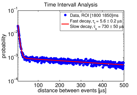
Time interval analysis (TIA) examines the temporal distance between neighboring events to draw conclusions on the statistical distribution of the atoms [49]. In contrast to the noise analysis presented in section 4.3, TIA does not require a series of measurements, but extracts statistical information from a single run of the experiment. Central to TIA is the probability to measure no counts in a time bin of size . For example: For independent counting events, such as multi-mode fluorescence from a constant source, is a constant and the probability of finding a time interval of bins that contain no photon counts is given by . It follows that is a linear function of for uncorrelated events.
The measured time interval distribution for atom detection events in our detector is shown in figure 8. It is composed of two superimposed exponential functions (red line, linear on the log scale of the graph). This suggests that we observe two distinct processes. An atom creates fluorescence counts according to its instantaneous fluorescence rate while it is present in the interaction region. After a certain time, characterized by the interaction time , the atom leaves the detection region. Except for random background counts with very low probability the detector sees no further light until the next atom arrives. Therefore, the steep slope for short time intervals is determined by the instantaneous fluorescence rate of individual atoms. For long time intervals the slope is given by the atom arrival rate.
In the experiments presented here we use thermal atoms in a multi-mode guide (typically transverse modes are occupied), thus their statistical distribution can be well approximated by a Poisson distribution. Indeed the linear relation between and for times shows that the atoms arrive independently from each other. Additionally equals the mean rate of atom detections, verifying a Poissonian distribution of arrival times in the multi-mode guide.
5.4 Photon antibunching

A single atom can emit only one photon at any given time. Before a second photon can be emitted, the atom has to be transferred to the excited state again. Therefore photon antibunching is expected to occur for single atom detection events at timescales of the order of the excited state lifetime ns [50, 51]. The second-order intensity correlation function is given by
| (3) |
Photon antibunching is characterized by , and for a single photon is expected.
For late arrival times larger than 1000 ms the atomic density in the guide is so low that collisional broadening and multi atom effects can be completely neglected. In this regime an approximation of for arbitrary probe beam powers can be given if the illumination is on resonance [51].
| (4) |
With and denoting the Rabi frequency.
For high efficiency atom detection a single SPCM is employed while correlation measurements require two SPCMs in Hanbury Brown-Twiss like configuration. Consequently for these measurements the light from the collection fiber is sent on to a 50/50 beam splitter, and both output ports are coupled to separate SPCMs (see Fig. 2). The counts from the SPCM are recorded and timestamped at 1 ns resolution by a multichannel counter card (FAST ComTec P7888 Multiscaler) in a dedicated computer. Special care has to be taken to compensate for secondary emission effects in the SPCMs.
Figure 9(a) shows three different measurements of from the cross-correlation of photon counts in two SPCMs in a Hanbury Brown-Twiss type setup for Rabi frequencies ranging from to . The correlation function was reconstructed from the low density tail of the atom distribution where the mean atomic distance is large enough to guarantee the presence of at most one atom in the detection region at any given time. We find beautiful agreement between the measurements and the theoretically predicted shapes according to equation 4. For Rabi oscillations in the correlation function can be clearly observed. We extract a value of from 4400 single measurements at . The total photon count rate for this measurement was approximately 3500 cps. If coincidental background correlations are corrected for the correlation reduces to even , demonstrating that we are able to observe near-perfect photon antibunching in the emission of single atoms passing the detector. This is a clear proof that our detector is capable of detecting single atoms in passage.
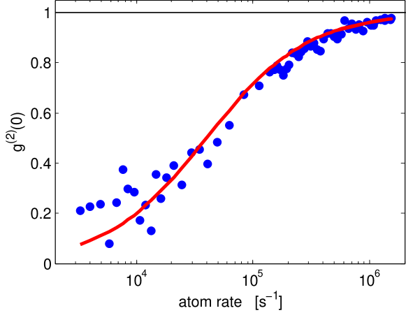
Our detector allows us to examine the photon antibunching as function of the atom density by evaluating as function of the arrival time, as the atom pulse passes the detector (compare the signal shape in figure 3(a)). For a single-mode field with mean photon number the second-order correlation at lag 0 is limited by [51]
| (5) |
while for the lower limit is 0. For a Fock state with fixed photon number the inequality (5) becomes an equality and the minimal value of is reached. While for classical light sources holds, the region is exclusively non-classical and can only be reached by quantum emitters.
Since is evaluated when at least one photon count has been recorded, the mean photon number has to be calculated under the condition . This leads to with mean atom number emitting. Hence is limited by
| (6) |
As can be seen from figure 10 the measured follows the expected shape for the full atom pulse duration. With this measurement we extend the original experimental investigation [50, 52] of the influence of atomic density on the second-order correlation function over almost three orders of magnitude change in atomic density.
6 Future improvements
The detection efficiency of the current detector setup is mainly limited by the photon collection efficiency given by the numerical aperture NA= of the multi-mode collection fiber. The detection efficiency can be significantly improved by increasing .
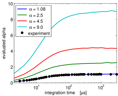 ,
,
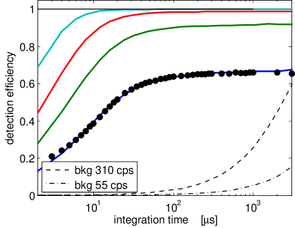
A single atom detection efficiency close to unity can be achieved by substituting the present detection fiber (NA=0.27) by a fiber with NA=. This increases the photon collection efficiency to %, which would result in counts per atom (see table 3). Such an improved system is expected to reach even at 50 kHz bandwidth a single atom detection efficiency of .
The detection efficiency can be further improved by collecting light from two sides by mounting two facing high NA detection fibers. Using two NA=0.53 fibers one can reach at integration times below . For such a detector system a signal strength of cpa is expected.
With either improvement implemented, high fidelity atom counting (in the sense of identifying the number of simultaneously present atoms) and observation of atom transits in transient count rate analysis will become feasible.
| [cpa] | SNR | |||
|---|---|---|---|---|
7 Conclusion
To conclude, we have built and evaluated an optical fiber-based atom detector which is fully integrated on an atom chip, alignment free by fabrication, and mechanically very robust and capable of state selective single atom detection at an efficiency of by counting fluorescence photons. It enables spatially and spectral highly selective probing while at the same time offering extremely robust operation. The total background is dominated by the dark count rate of the employed SPCMs. High efficiency detection is possible as well as low noise, high bandwidth detection. At 20 s integration time single atom detection can be performed at an efficiency of . The disadvantage of fluorescence detection is the destructive nature of the process, which our detector shares with photon detection. Our detector can therefore be best characterized as the atom optic equivalent of an avalanche photo diode type SPCM.
Low noise, high efficiency and insensitivity to stray light is achieved using fiber optics to create very selective excitation of the atoms in a small, matched observation volume.
The detection efficiency is currently limited by the numerical aperture of the multimode collection fiber. A straightforward substitution of the employed NA=0.275 fiber by a commercially available fiber with NA=0.53 increases the photon collection to = 4.5 counts/atom and the single atom detection efficiency to 95% at 50 kHz bandwidth. Employing two collection fibers = 9 cpa and at integration times below can be achieved. With these improvements, full atom counting becomes feasible.
The high efficiency, signal-to-noise ratio and bandwidth of our integrated detector make it suitable for many physical systems where only a few photons can be scattered. A prime example would be detecting trapped cold molecules. With its extremely low sensitivity to stray light, our detector is well suited for studies of correlated atomic systems and scalable quantum experiments on a single-atom or molecule level.
References
References
- [1] G. S. Hurst, M. H. Nayfeh, and J. P. Young. Appl. Phys. Lett., 30 229, 1977.
- [2] A. Öttl, St. Ritter, M. Köhl, and T. Esslinger. Phys. Rev. Lett., 95 090404, 2005.
- [3] T. Aoki, B. Dayan, E. Wilcut, W. P. Bowen, A. S. Parkins, T. J. Kippenberg, K. J. Vahala, and H. J. Kimble. Nature, 443 671, 2006.
- [4] C. J. Hood, T. W. Lynn, A. C. Doherty, A. S. Parkins, and H. J. Kimble. Science, 287 1447, 2000.
- [5] P. Münstermann, T. Fischer, P. Maunz, P. W. H. Pinkse, and G. Rempe. Phys. Rev. Lett., 82 3791, 1999.
- [6] H. Mabuchi, Q. A. Turchette, M. S. Chapman, and H. J. Kimble. Opt. Lett., 21 1393, 1996.
- [7] H. Mabuchi, J. Ye, and H.J. Kimble. Appl. Phys. B, 68 1095, 1999.
- [8] A. Haase, B. Hessmo, and J. Schmiedmayer. Opt. Lett., 31 268, 2006.
- [9] I. Teper, YJ Lin, and V. Vuletić. Phys. Rev. Lett., 97 023002, 2006.
- [10] M. Trupke, J. Goldwin, B. Darquié, G. Dutier, S. Eriksson, J. Ashmore, and E. A. Hinds. Phys. Rev. Lett., 99 063601, 2007.
- [11] Y. Colombe, T. Steinmetz, G. Dubois, F. Linke, D. Hunger, and J. Reichel. Nature, 450 272, 2007.
- [12] Y. Miroshnyenko, D. Schrader, S. Kuhr, W. Alt, I. Dotsenko, M. Khudaverdyan, A. Rauschenbeutel, and D. Meschede. Opt. Express, 11 3498, 2003.
- [13] B. Darquie, M. P. A. Jones, J. Dingjan, J. Beugnon, S. Bergamini, Y. Sortais, G. Messin, A. Browaeys, and P. Grangier. Science, 309 454, 2005.
- [14] F. Diedrich and H. Walther. Phys. Rev. Lett., 58 203, 1987.
- [15] D. Leibfried, R. Blatt, C. Monroe, and D. Wineland. Rev. Mod. Phys., 75 281, 2003.
- [16] D. Leibfried, M. D. Barrett, T. Schaetz, J. Britton, J. Chiaverini, W. M. Itano, J. D. Jost, C. Langer, and D. J. Wineland. Science, 304 1476, 2004.
- [17] T. Bondo, M. Hennrich, T. Legero, G. Rempe, and A. Kuhn. Opt. Commun., 264( 271, 2006.
- [18] M. L. Terraciano, R. Olson Knell, D. G. Norris, J. Jing, A. Fernandez, and L. A. Orozco. Nat. Phys., 5 480, 2009.
- [19] R. Folman, P. Krüger, D. Cassettari, B. Hessmo, T. Maier, and J. Schmiedmayer. Phys. Rev. Lett., 84 4749, 2000.
- [20] R. Folman, P. Kruger, J. Schmiedmayer, J. Denschlag, and C. Henkel. Adv. At. Mol. Opt. Phys., 48 263, 2002.
- [21] J. Reichel. Appl. Phys. B, 75 469, 2002.
- [22] J. Fortagh and C. Zimmermann. Rev. Mod. Phys., 79 235, 2007.
- [23] P. Krüger et al. Phys. Rev. Lett., 91 233201, 2003.
- [24] W. Hänsel, J. Reichel, P. Hommelhoff, and T. W. Hänsch. Phys. Rev. Lett., 86 608, 2001.
- [25] D. Cassettari, B. Hessmo, R. Folman, T. Maier, and J. Schmiedmayer. Phys. Rev. Lett., 85 5483, 2000.
- [26] H. Ott, J. Fortagh, G. Schlotterbeck, A. Grossmann, and C. Zimmermann. Phys. Rev. Lett., 87 230401, 2001.
- [27] W. Hänsel, P. Hommelhoff, T.W. Hänsch, and J. Reichel. Nature, 413 498, 2001.
- [28] S. Schneider et al. Phys. Rev. A, 89 023612, 2003.
- [29] T. Schumm et al. Nature Physics, 1:57, 2005.
- [30] P. Bohi, M. F. Riedel, J. Hoffrogge, J. Reichel, T. W. Hansch, and P. Treutlein. Nat Phys, 5 592, 2009.
- [31] D. Gallego, S. Hofferberth, T. Schumm, P. Krueger, and J. Schmiedmayer. Opt. Lett., 34 3463, 2009.
- [32] J. Denschlag et al. Appl. Phys. B, 69 291, 1999.
- [33] B. Grüner, M. Jag, A. Stibor, G. Visanescu, M. Häffner, D. Kern, A. Günther, and J. Fortágh. Phys. Rev. A, 80 063422, 2009.
- [34] A. Günther, H. Bender, A. Stibor, J. Fortágh, and C. Zimmermann. Phys. Rev. A, 80 011604, 2009.
- [35] P. Quinto-Su, M. Tscherneck, M. Holmes, and N. Bigelow. Opt. Express, 12 5098, 2004.
- [36] M. Wilzbach, D. Heine, S. Groth, X. Liu, T. Raub, B. Hessmo, and J. Schmiedmayer. Opt. Lett., 34 259, 2009.
- [37] P. G. Petrov R. A. Nyman M. Trupke E. A. Hinds M. Kohnen, M. Succo. arXiv:0912.4460v1, 2009.
- [38] P. Horak, B. G. Klappauf, A. Haase, R. Folman, J. Schmiedmayer, P. Domokos, and E. A. Hinds. Phys. Rev. A, 67 043806, 2003.
- [39] S. Groth, P. Krüger, S. Wildermuth, R. Folman, T. Fernholz, J. Schmiedmayer, D. Mahalu, and I. Bar-Joseph. Appl. Phys. Lett., 85 2980, 2004.
- [40] M. Trinker, S. Groth, S. Haslinger, S. Manz, T. Betz, S. Schneider, I. Bar-Joseph, T. Schumm, and J. Schmiedmayer. Appl. Phys. Lett., 92 254102, 2008.
- [41] X. Liu, K.-H. Brenner, M. Wilzbach, M. Schwarz, T. Fernholz, and J. Schmiedmayer. Appl. Opt., 44 6857, 2005.
- [42] D. Heine, M. Wilzbach, T. Raub, B. Hessmo, and J. Schmiedmayer. Phys. Rev. A, 79 021804, 2009.
- [43] A. del Campo and C. Greiner. Journal of Micromechanics and Microengineering, 17 R81–R95, 2007.
- [44] M. Wilzbach et al. Fortschr. Phys., 54 746, 2006.
- [45] E.R.I. Abraham and E. A. Cornell. Appl. Opt., 37 1762, 1998.
- [46] S. Wildermuth et al. Phys. Rev. A, 69 030901, 2004.
- [47] W. Rohringer et al. Appl. Phys. Lett., 93 264101, 2008.
- [48] L. Mandel and E. Wolf. Rev. Mod. Phys., 37 231, 1965.
- [49] M. Köhl, A. Öttl, S. Ritter, T. Donner, T. Bourdel, and T. Esslinger. Appl. Phys. B, 86 391, 2007.
- [50] H. J. Kimble, M. Dagenais, and L. Mandel. Phys. Rev. Lett., 39 691, 1977.
- [51] R. Loudon. The Quantum Theory of Light. Oxford Science, 3rd edition, 2000.
- [52] H. J. Kimble, M. Dagenais, and L. Mandel. Phys. Rev. A, 18 201, 1978.