Excitonic effects in the optical properties of CdSe nanowires
Abstract
Using a first-principle approach beyond density functional theory we calculate the electronic and optical properties of small diameter CdSe nanowires. Our results demonstrate how some approximations commonly used in bulk systems fail at this nano-scale level and how indispensable it is to include crystal local fields and excitonic effects to predict the unique optical properties of nanowires. From our results, we then construct a simple model that describes the optical gap as a function of the diameter of the wire, that turns out to be in excellent agreement with experiments for intermediate and large diameters.
Nanowires (NW) exhibit a wide range of unique properties intro-05.Review , including tunable band gaps, ballistic transport intro-09 , optical anisotropy CdSe-exp01 and strong excitonic effects intro-08.Nature . It is therefore not surprising that for the past twenty years NW have emerged as one of the most active fields of research in material science intro-05.Review . This growing interest is mainly due to their short term promising applications intro-09 ; intro-06 ; intro-08.Nature and is empowered by a strong demand from industries for smaller and more effective devices. To a large extent, the novel properties emerge from the lateral confinement of the electrons in the wire, leading to the blue shift of the electronic band gap with decreasing diameter.
In this article we focus on the optical properties of CdSe NW from a first-principle perspective, based and going beyond standard density functional theory (DFT). Beside analyzing how optical properties evolve with the diameter of the wire, we test some approximations that are commonly used for bulk materials and discuss their applicability to electronic excitations in 1D systems. Several studies of the optical properties of CdSe wires have appeared in the past years CdSe-theo.semiempiricalo ; cdse-theo1 ; CdSe-theo.semiempiricalF . Classical CdSe-exp01 and semi-empirical CdSe-theo.semiempiricalF methods have been quite successful in describing large-diameter wires, but they fail for small and medium diameters. Furthermore, none of articles using first-principle methods present in the literature CdSe-theo.semiempiricalo ; cdse-theo1 was capable of capturing the physics of electronic excitations in these confined systems. This was due to the neglect of at least one of the following physical effects that are fundamental for an accurate description of nano-scale objects:
(a) Crystal local-field effects. When the polarization of the light is perpendicular to the long axis there is an accumulation of charges at the wire surface, which in turn is responsible for the attenuation of the electric field inside the NW. This leads to a strong suppression of the absorption for light polarized perpendicular to the NW axis, increasing dramatically the optical anisotropy of the system Marinopoulos2003 ; *Bruneval2005-comm. This huge effect has already been measured CdSe-exp01 in polarized photo-luminescence experiments, but unfortunately some recent theoretical works cdse-theo1 ; SiNW still neglect it.
(b) Electron-electron interaction and excitonic effects. These effects are very pronounced in semi-conducting NW due to the attenuation of the screening. The strong electron-hole binding is responsible for a red shift of the fundamental absorption frequency. Due to this effect, NW can be seen as exciton traps, a property that endows them of great technological interest intro-08.Nature .

To study the importance of local-field corrections, we calculated the absorption spectra of unpassivated CdSe NW of 5 different diameters (0.73, 1.17, 1.59, 1.77, and 2.01 nm) starting from DFT Kohn-Sham states and applying the random-phase approximation (RPA) to obtain the dielectric tensor (for details on this and all the other approximations employed in the following, refer to Ref. botti-review-07, ). The neglect of local-field effects is equivalent to applying Fermi’s golden rule, i.e., to treat only independent particle transitions, and completely ignores the inhomogeneity in the dielectric response due to the reduced dimensionality of the nano-object.
All CdSe NW were assumed to be infinitely long with periodic length 7.01 Å and with their axis parallel to the wurtzite (001) axis. Ground state calculations were performed using the DFT code ABINIT Software-ABINIT1 , and the core electrons of Cd ([Kr]4d10) and Se ([Ar]3d10) were described by Hamann norm conserving pseudo-potentials. We chose the Perdew-Burke-Ernzerhof PBE approximation to the exchange-correlation functional. Converged calculations required a cutoff energy of 20 Ha and a Monkhorst-pack sampling of the Brillouin zone. Atomic positions were relaxed starting from the bulk wurtzite structure. The converged spacing between the wires in our supercell approach was at least 7 Å.
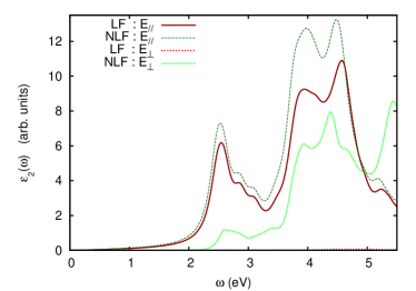
The optical spectra of the wire with 0.73 nm, calculated at the RPA level including or neglecting local fields is shown in Fig. 1 . Without local fields, there is a small anisotropy between the absorption perpendicular and parallel to the NW axis, comparable to the anisotropy in bulk CdSe. However, and as expected, turning on local-field effects suppresses completely the low energy absorption peaks in the perpendicular direction, rendering the wire almost transparent below 6.5 eV. This optical anisotropy, in agreement with experimental results CdSe-exp01 , clearly decreases with the diameter, but it is known to be still relevant for NW with a diameter of 100 nm.

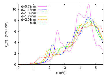
To observe how the optical properties vary with diameter, we plot the RPA spectrum (including local fields) for five small wires in Fig. 2 . It is expected that the RPA gives a poor quantitative result due to the inappropriate treatment of electron-electron and electron-hole interactions, but it is however possible to extract qualitative trends thanks to the partial cancellation of these two terms (see below). We see that increasing the diameter, and thereby decreasing the confinement effect, leads to a red-shift of the spectrum, with the absorption threshold moving towards the RPA bulk value. There is also a redistribution of the oscillator strengths, with the first peak loosing intensity.

To go beyond the RPA and to include the relevant missing contributions, we performed calculations solving the Bethe-Salpeter equation (BSE) Onida2002 and using time-dependent DFT botti-review-07 — both in the adiabatic local density approximation (ALDA) and with the model long range (LRC) kernels Other-LRCab ; *Other-LRCa derived from the BSE. The BSE approach is the state-of-the-art method for calculations of optical absorption and gives results in excellent agreement with experiments Onida2002 ; botti-review-07 . For the LRC and BSE calculations, one requires as a starting point the quasi-particle band structure, usually obtained within the GW approximation Hedin1965 . Note that the GW approximation predicts accurate band gap energies for CdSe, in contrast with the systematic underestimation of the gap obtained in DFT. Unfortunately, GW calculations are computationally demanding, even for the small wires studied here. We therefore used the following approach to obtain the quasi-particle corrections: we solved the GW equations for our smallest NW ( nm), and then used a simple theoretical model Other-Model based on crystal field theory to interpolate between this result and the GW gap of the bulk cdse-theo4.Angel .
The GW calculations were performed with ABINIT, applying the standard plasmon-pole approximation. An energy cutoff for the dielectric matrix of 9 Ha and the technique of Ref. Other-Bruneval.trick, to reduce the number of unoccupied states in the sums over states were employed. Despite the use of a cylindrical cutoff for the Coulomb interaction Other-Beigi , a distance of 10 Å between the wires was required to converge the GW corrections to the Kohn-Sham band structure. These corrections turned out to be quite insensitive to the -point and band index, in agreement with other results for Si and Ge NW Other-Si.NW ; Other-Ge.NW , and in contrast with findings for graphene nanoribbons Other-Nribons.S.louie . The GW gap for the smallest wire was eV, and the final form of the model relating the quasi-particle gap with the diameter of the wire ( in nm) turned out to be (eV).
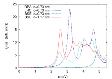
The BSE results (see Fig. 3), obtained using the code YAMBO Software-YAMBO , prove the existence of strong excitonic effects, with the excitonic peaks in the visible energy range. The excitonic binding energy compensates almost entirely the large blue-shift coming from the quasi-particle corrections, and leads to a transfer of the oscillator strength from the higher energy absorption peaks to the first peak. On the other hand, the LRC kernels derived from the BSE, that yield results comparable to the solution of the BSE for bulk CdSe Other-LRCab , fail dramatically for NW — in fact, as shown in Fig. 3 , even the optical gap resulting from DFT+RPA calculation is in better agreement with the BSE result. The attempt to increase the excitonic effect by modulating the empirical parameters of the LRC kernel did not lead to improvements. The reason is that the simple LRC approximations are only valid for delocalized excitons, but fail to reproduce the considerable binding energy of the very localized excitons existing in NW.
The exciton binding energies from BSE calculations, for the NW with diameters of 0.73 and 1.17 nm are respectively 1.6 and 1.13 eV. These values are much larger than the binding energy in bulk CdSe intro-08.Nature , 5.1 meV, and almost twice as large as the ones found in carbon nanotubes nanotubes . The decrease of the binding energy with the NW diameter, also followed by a transfer of the intensity of the absorption-edge peak to the higher energy ones (see Fig. 3), reflects the weakening of the excitonic effects with the increasing of the exciton spatial extent. In fact, the exciton radius of bulk CdSe is 5.6 nm intro-08.Nature : A nano-object where one of its dimensions is smaller than this value will have strongly bound excitons, due to a large overlap between electron and hole. Furthermore one expects that the larger the confinement the larger is the excitonic binding energy. In our BSE results we also found spin singlet dark excitons throughout the spectra, with the first one appearing at 3.2 eV for the smallest wire. This dark exciton may play a role in non-radiative decay processes and thus affect the luminescence properties.

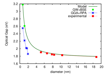
Based on our BSE results for the two smallest wires and on the experimental optical gap of the bulk CdSe-exp02 , we constructed a simple model to interpolate the optical gaps of CdSe NW. The form is the same as the previous model for the GW gaps, and the formula connecting optical gaps and the diameter of the wire turns out to be (eV). We can see, from Fig. 4 , that this model describes extremely well the experimental results CdSe-exp02 not only for large NW but also in the intermediate regime. Finally, from Fig. 4 we conclude that although the RPA results are red-shifted with respect to the latter they still conserve approximately the correct slope.
In conclusion, the first-principle calculations reported here show how indispensable is the inclusion of local-field and excitonic effect to describe quantitatively the optical response of CdSe NW. In fact, calculations based on the Fermi’s golden rule will never be able to catch the physics arising from the low dimensionality of the system, which is at the heart of the novel properties of NW. We have then provided a simple model for the dependency of the optical gap with diameter, which is in excellent agreement with available experimental results. Furthermore we have observed the failure of long-range model kernels of time-dependent density functional theory for these nano-scale systems, in spite of their success in the calculation of the optical properties of bulk CdSe.
SB acknowledges support from EU’s 7th Framework Programme (e-I3 contract ETSF), MALM from the Portuguese FCT (PTDC/FIS/73578/2006) and the French ANR (ANR-08-CEXC8-008-01), JGV from the FCT (SFRH/BD/38340/2007). Calculations were performed at the LCA of the University of Coimbra and at GENCI (project x2009096017).
References
- (1) M. Law, J. Goldberger, and P. Yang, Annu. Rev. Mater. Sci. 34, 83 (2004).
- (2) D. J. Sirbuly, M. Law, H. Yan, and P. Yang, The journal of Physical Chemistry B 109, 15190 (2005).
- (3) C. X. Shan, Z. Liu, and S. K. Hark, Phys. Rev. B 74, 153402 (2006).
- (4) G. D. Scholes and G. Rumbles, Nat. Mater. 5, 683 (2006).
- (5) Y. Li, F. Qian, J. Xiang, and C. M. Lieber, Mater. Today 9, 18 (2006).
- (6) J. Li and L.-W. Wang, Phys. Rev. B 72, 125325 (2005).
- (7) S. P. Huang, W. D. Cheng, D. S. Wu, J. M. Hu, J. Shen, Z. Xie, H. Zhang, and Y. J. Gong, Appl. Phys. Lett. 90, 135301 (2007).
- (8) Q. Zhao et al., Nano Lett. 7, 3274 (2007).
- (9) A. G. Marinopoulos, L. Reining, A. Rubio, and N. Vast, Phys. Rev. Lett. 91, 046402 (2003).
- (10) F. Bruneval, S. Botti, and L. Reining, Phys. Rev. Lett. 94, 219701 (2005).
- (11) X. Zhao, C. M. Wei, L. Yang, and M. Y. Chou, Phys. Rev. Lett. 92, 236805 (2004).
- (12) S. Botti et al., Rep. Prog. Phys. 70, 357 (2007).
- (13) X. Gonze et al., Comput. Mater. Sci. 25, 478 (2002).
- (14) J. P. Perdew, K. Burke, and M. Ernzerhof, Physical Review Letters 77, 3865 (Oct. 1996).
- (15) G. Onida et al. 74, 601 (2002).
- (16) S. Botti et al., Phys. Rev. B 72, 125203 (2005).
- (17) S. Botti et al., Phys. Rev. B 69, 155112 (2004).
- (18) L. Hedin, Phys. Rev. 139, A796 (1965).
- (19) S. Li and G. W. Yang, Appl. Phys. Lett. 95, 073106 (2009).
- (20) O. Zakharov et al., Phys. Rev. B 50, 10780 (1994).
- (21) F. Bruneval and X. Gonze, Phys. Rev. B 78, 085125 (2008).
- (22) S. Ismail-Beigi, Phys. Rev. B 73, 233103 (2006).
- (23) X. Zhao, C. M. Wei, L. Yang, and M. Y. Chou, Phys. Rev. Lett. 92, 236805 (2004).
- (24) M. Bruno, M. Palummo, A. Marini, R. D. Sole, V. Olevano, A. N. Kholod, and S. Ossicini, Phys. Rev. B 72, 153310 (2005).
- (25) L. Yang, M. L. Cohen, and S. G. Louie, Nano Lett. 7, 3112 (2007).
- (26) A. Marini, C. Hogan, M. Grüning, and D. Varsano, Comput. Phys. Comm. 180, 1392 (2009).
- (27) C. D. Spataru et al., Phys. Rev. Lett. 92, 077402 (Feb 2004).
- (28) H. Yu, J. Li, R. A. Loomis, P. C. Gibbons, Wang, and W. E. Buhro, J. Am. Chem. Soc. 125, 16168 (2003).