Photonic Crystal Nanobeam Cavity Strongly Coupled to the Feeding Waveguide
Abstract
A deterministic design of an ultrahigh Q, wavelength scale mode volume photonic crystal nanobeam cavity is proposed and experimentally demonstrated. Using this approach, cavities with Q and on-resonance transmission T90% are designed. The devices fabricated in Si and capped with low-index polymer, have Q=80,000 and T=73%. This is, to the best of our knowledge, the highest transmission measured in deterministically designed, wavelength scale high Q cavities.
Photonic crystal (PhC)Yablonovitch87 John87 cavities, with quality(Q) factors over million and wavelength scale mode volumes, are widely applied in the fields that range from quantum information processing and nonlinear optics, to biomedical sensing. The fourier space analysisVuckovic02 Katik02 , the multi-pole cancelationJohnson01 , and the mode matching mechanismwatts02 lalanne01 lalanne04 have been developed to explain the origin of high Qs. The design of PhC cavities, however, is typically based on extensive parameter search and optimizationNoda03 -Notomi08 , also known as intuitive design. The large computational cost, in particular the computation time, needed to perform the simulation of high-Q cavities make this trial based method inefficient. Inverse engineering design, in which the physical structure is optimized by constructing specific target functions and constraints, was also proposedgeremia02 Burger04 . A design recipe based on the desired field distribution is proposed in Dirk05 . In this letter, we propose and experimentally demonstrate a deterministic method to design an ultrahigh Q, sub-wavelength scale mode volume, PhC nanobeam cavity(Figure.1) that is strongly coupled to the feeding waveguide(i.e. near unity on resonance transmission). The design approach is deterministic in the sense that it does not involve any trial-based hole shifting, re-sizing and overall cavity re-scaling to ensure ultra-high Q cavity. Moreover, the final cavity resonance has less than 2% deviation from a predetermined frequency. Our design method requires only computationally inexpensive, photonic band calculations (e.g. using plane wave expansion method), and is simple to implement.
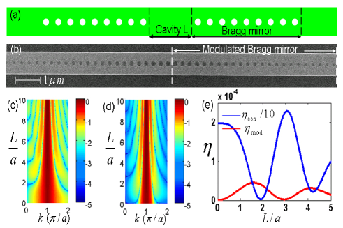
The Q factor of a PhC nanobeam cavity can be maximized by reducing the out-of plane scattering() due to the coupling to the radiation modes. As shown previouslyVuckovic02 Dirk05 , scattered power () can be expressed as an integral of spatial fourier frequencies within a light cone, calculated over the surface above the cavity: . The integral is minimized when major fourier components are tightly localized (in k-space) at the edge of the first Brillioun zoneKatik02 . We start by considering the ideal field distribution on this surface which would minimize . A general property of these nanobeam cavities is that it consists of the waveguide region of length L, that supports propagating modes, surrounded by infinitely long Bragg mirror on each side(Figure.1a). Without the loss of generality, we consider the TE-like cavity mode with Hz as a major field component. In the case of conventional periodic Bragg mirror, evanescent field inside the mirror can be expressed as , where is attenuation constant. The cavity field inside the waveguide region can be represented as . As mentioned above, scattering loss decreases in mirror section when , while phase matching between mirror and waveguidelalanne01 , , minimizes the scattering loss at cavity-mirror interface. The spatial fourier transform of such cavity field is approximately a Lorentzian in the vicinity of . As proposed in Noda03 , spatial frequencies within light-cone can be minimized (Q maximized) if the field attenuation inside the mirror has a Gaussian shape . In Figure 1(c)&(d), the fourier space spectrums of the cavity modes with exponential and with Gaussian attenuation are shown respectively. The fraction of the energy associated with spatial harmonics within the light-cone, , for both cases is shown in Figure.1(e). It can be seen that cavity with the Gaussian attenuation has more than an order of magnitude smaller .
The preferred Gaussian attenuation can be obtained by making a linearly increasing function of the position within the mirror(). We name such mirror ”modulated Bragg mirror”. At the same time, to prevent scattering, the oscillating part of the field, , should have constant throughout the mirror. This condition is satisfied only if each segment of modulated Bragg mirror has the same length (”periodicity”) , and if the operating frequency is kept inside the bandgap of each segment of the modulated Bragg mirror. In the case of dielectric-mode cavity, this can be achieved by lowering the band-edges of each modulated mirror segment in a way that linearly increases the mirror strength. Moreover, the optimal cavity length for this type of cavity is from Figure.1(b), which simultaneously minimizes the mode volume () of the cavity and thus increases . It is worth noting that in Figure.1(b) corresponds to the so-called L3 cavityNoda03 .
One way to make ”modulated Bragg mirror” is to linearly decrease the filling factor(FF) in nanobeam cavity, which, as we show later, correspond to a linear increase in mirror strength around the cavity center. FF is defined as the ratio between the hole area and the area of the unit cell. Other types of modulation may exist that enable a linearly increasing mirror strength. In such structure, cavity resonance frequency is expected to be very close but slightly smaller than the dielectric band-edge of the the central segment. This is due to the reduction of the hole size in the modulated Bragg mirror, and can be estimated using perturbation theory. The difference decreases as the number of modulated mirror segments increases. To summarize the design principles we obtained so far: (i) zero cavity length (), (ii) the length of each segment be the same (period=a) result in constant phase velocity at and (iii) a modulated Bragg mirror results in Gaussian shaped field attenuation.
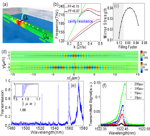
We demonstrate the power of the recipe by designing an ultra-high Q and small mode volume PhC nanobeam cavity that operates at (196.6THz) in a realistic geometry. We assume that the nanobeam is made with silicon-on-insulator material with 220nm thick Si device layer (constrained by our SOI wafer properties), and capped with silica: nanobeam is made of silicon (n=3.46), while holes, bottom and top cladding are made of material with (n=1.45) (air-holes backfilled with silica). Our design approach is as follows: (i)We choose the period a by selecting to be between and . is a good compromise, resulting in . We note, however, that any (and thus any periodicity) which opens a band gap can be used as a starting point to realize a high Q cavity, assuming that sufficiently slow modulation is used. (ii) Next, we choose the width of the nanobeam to be as wide as possible in order to push the mode away from the light-line, while still being single mode. Band diagram simulation shows that 700nm is an optimal choice, that keeps the second order mode (of the same symmetry as the fundamental one) at the edge of the banggap. (iii) Next, we find the proper FF which produces a dielectric band edge at . With , FF can be estimated using sakoda , which gives 0.19. Then numerical band diagram simulation shows the actual . Figure.2(b)&(c) shows the banddiagram and mirror strength at several FFs. The linear region between FF=0.15 and FF=0.09 can be used to construct the ”modulated Bragg mirror”. (iv) Finally, the nanobeam cavity needs to be strongly coupled to the feeding waveguide in order to achieve a large transmission efficiency when probing the cavity. The transmission at the cavity resonance can be written as johnson . Therefore, the cavity should be limited by . The linear decrease of the FF from 0.15 to 0 provides a natural way to achieve this. More sophisticated couplers will be discussed elsewhere. In the proposed design method, (i) - (iv), all cavity parameters are determined using fast band diagram calculations, only. We note, that the most critical part of our method is that the modification of the periodic photonic crystal is achieved by keeping the periodicity constant, modulating the filing fraction and using zero cavity length. This approach preserves the phase velocity of each segment and is essential for realization of high-Q cavities. Our design strategy has an additional important advantage over other types of photonic crystal nanobeam cavitiesNoda03 -Notomi06 ,Deotare08 -painter : it provides a natural way to efficiently over-couple the cavity to the feeding waveguide. Again, we stress that these high Qs are obtained by-design, performing only simple band-diagram calculations, and no additional parameter-search trial-based method was performed. This significantly reduces the computational time to a few minutes, while a full FDTD simulation takes more than 24 hours using a grid with 64 processors.
| type | () | Trans. | ||||
|---|---|---|---|---|---|---|
| mod40 | 1.552 | 2.2E7 | 1.3E6 | 1.2E6 | 1.1 | 0.91 |
| mod50 | 1.549 | 2.5E7 | 2.2E7 | 1.2E7 | 1.2 | 0.53 |
To verify our designs, 3D FDTD modeling is used to study the cavity with above mentioned parameters. The results are summarized in Table.1 for two cavities with 40 and 50 modulated mirror segments on each side. It can be seen that cavities feature ultra-high Qs (both and ). At the same time, high transmission, particularly in cavity ”mod40”, is obtained. In principle, Qs can be arbitrarily high by applying sufficient slow modulation, at the cost of larger mode volumes. However, in practical case, cavity Q is limited by material losses and fabrication precisions, and therefore, Q of tens of millions is sufficient.
To experimentally verify our designs, we fabricated waveguide-coupled cavity ”mod40” using a silicon-on-insulator(SOI) wafer with a 220nm device layer on a 2um buried oxide, using the fabrication procedure described in our previous workDeotare08 . Spot size converterIBM , that consists of (cross section) polymer pad() was used to couple light in and out of the cavities. The devices were embedded in polymer with refractive index . The reduction of refractive index of top cladding from the simulated one () slightly affects our cavity design. We modeled devices with polymer top cladding and found that the cavity resonance is shifted to shorter wavelength (), the cavity is 2.72E6, and the the on-resonance transmission is .
We characterized the device using a tunable laser source(1470-1580nm) and a tapered fiber tip(2.5m spot diameter) to couple light in and out of the polymer waveguide. A polarizer is placed at the output to filter out the TM-like mode. Figure.2(e) is the experiment transmission spectrum through one of the resonators. The signal is normalized by the band-edge modes, which has a unity transmission as verified by 3D FDTD simulations (inset). A nonlinear bistability is observed and Figure.2(f) further shows the zoom in of the fundamental mode at different input power levels. We fitted the experimental data using the following expression typical for the nonlinear bistability
| (1) |
is the characterized power in the presence of a third order nonlinearity. is the nonlinear feedback parameter introduced by Soljacic et. alsoljacic02 . is an indicator of the extent of the field that is confined in the nonlinear region. is the natural cavity linewidth. We obtained a and an on-resonance transmission for the on-substrated and capped cavity. This corresponds to a , which is comparable with our previously reported results for free-standing photonic crystal nanobeam cavityDeotare08 . The demonstrated transmission is much higher than previous works with the same QNotomi09 .
In summary, we proposed and demonstrated a deterministic design of the high Q PhC nanobeam cavities. Our cavities are ideally suited for the coupling to the feeding waveguides and allow for high transmission efficiency. This makes them ideal candidates for the realization of densely integrated photonic systems, and are suitable for applications ranging from optical interconnects to biochemical sensors. Finally, record high Q/V ratios of photonic crystal nanobeam cavities will enable further fundamental studies in spontaneous emission control, nonlinear optics and quantum optics.
Acknowledgements.
We acknowledge useful discussions with M.W. MuCutcheon. This work is supported by NSF Grant No. ECCS-0701417 and NSF CAREER grant. Device fabrication is performed at the Center for Nanoscale Systems(CNS) at Harvard.References
- [1] E. Yablonovitch, Phys. Rev. Lett. 58, 2059-2062 (1987)
- [2] S. John, Phys. Rev. Lett. 58, 2486 (1987)
- [3] J. Vuckovic, M. Loncar, H. Mabuchi, & A. Scherer, IEEE Journal of Quantum Electronics, 38, 850-856 (2002)
- [4] K. Srinivasan, & O. Painter, Optics Express 10, 670-684 (2002)
- [5] S. G. Johnson, S. Fan, A. Mekis, & J. D. Joannopoulos, Appl. Phys. Lett. 78, 3388-3390 (2001)
- [6] M. R. Watts, S. G. Johnson, H. A. Haus, & J. D. Joannopoulos, Optics Letters, 27, 1785-1787 (2002)
- [7] M. Palamaru, & P. Lalanne, Appl. Phys. Lett. 78, 1466-1468(2001)
- [8] P. Lalanne, S. Mias, & J. P. Hugonin, Optics Express 12, 458-467 (2004)
- [9] Y. Akahane, T. Asano, B. S. Song, & S. Noda, Nature 425, 944-947 (2003)
- [10] B. S. Song, S. Noda, T. Asano, & Y. Akahane, Nature Materials 4, 207-210(2005)
- [11] S. Tomljenovic-Hanic, C. M. de Sterke, & M. J. Steel, Optics Express 14, 12451-12456 (2006)
- [12] E. Kuramochi et. al., Appl. Phys. Lett. 88, 041112 (2006)
- [13] M. Notomi, E. Kuramochi, and H. Taniyama, Optics Express, 16, 11095(2008)
- [14] J. M. Geremia, J. Williams & H. Mabuchi, Phys. Rev. E 66, 066606(2002)
- [15] M. Burger, SJ Osher, and E. Yablonovitch, IEICE Trans. Electron. E87C, 258 C265 (2004).
- [16] D. Englund, I. Fushman & J. Vuckovic, Optics Express 13, 5961-5975 (2005)
- [17] K. Sakoda, ”Optical Properties of Photonic Crystals”, 2nd Edition, Springer (2005)
- [18] P. B. Deotare et. al, Appl. Phys. Lett, 94, 121106 (2009)
- [19] M. W. McCutcheon & M. Loncar, Optics Express 16, 19136-19145 (2008)
- [20] Y. Zhang & M. Loncar, Optics Express 16, 17400-17409 (2008)
- [21] J. Chan, M. Eichenfield, R. Camacho & O. Painter, Optics Express 17, 3802-3817(2009)
- [22] J. D. Joannopoulos, S. G. Johnson, J. N. Winn, R. D. Meade, ”Photonic Crystals: Molding the flow of light”, 2nd Edtition, Cambridge University Press (2007)
- [23] S. J. McNab, N. Moll and Y. A. Vlasov, Optics Express 11, 2927(2003)
- [24] M. Soljacic, M. Ibanescu, S. G. Johnson, Y. Fink and J. D. Joannopoulos, Phys. Rev. E 66, 055601(R) (2002)
- [25] L. Haret, T. Tanabe, E. Kuramochi & M. Notomi, Optics Express 17, 21109(2009)