Plasmonic crystal demultiplexer and multiports
††preprint: DRAFTArtificially built periodic optical structures in dielectric and metallic media have generated considerable interest due to their potential for optical device miniaturization PC ; Smith ; Barnes:2003 ; Ebbesen . In this context plasmonics, i.e., optics based on surface plasmon polaritons (SPPs) Barnes:2003 offers new exciting prospects. SPPs are hybrid light/electron surface waves at the interface between a dielectric and a metal Raether:1988 and as such hold the potential for 2D optical functionality. Indeed, SPP elements as mirrors, splitters and interferometers have been recently demonstrated Ditlbacher:2002 ; Weeber:2005 ; Stepanov:2005 ; Drezet:2005 ; Drezet:2006 . However, for plasmonics to qualify at the information technology level requires necessarily the realization of wavelength division (demultiplexing) which constitutes a fundamental ingredient of optical communication. In the following we experimentally demonstrate 2D SPP demultiplexing in the visible spectral range by using photonic crystals for SPPs (plasmonic crystals). In addition, we demonstrate that plasmonic crystal are capable of realizing integrated linear multiports which could constitute building blocks of analog or quantum optical computing.
The introduction of 2D plasmonic crystals creates new opportunities for nanooptics since such metal-based structures can generate huge optical band gaps Weeber:2006 . Indeed, complete SPP confinement (i. e., an all-angle optical band gap) has been demonstrated Barnes:1996 which opens up a venue for SPP based waveguiding Bozhevolnyi:2001 . Simpler geometries as 1D plasmonic band gap structures (Bragg mirrors or gratings) are already well mastered, typical SPP Bragg reflectors being built from periodically arranged lines of nanoscale metal protrusions or indentations on a metal film Ditlbacher:2002 ; Weeber:2005 . Bragg diffraction occurs when the in–plane wave vector of the incoming SPP wave can pick up a momentum . is a reciprocal vector of the Bragg lattice oriented along the periodicity direction of the mirror, is the lattice period and p is an integer. The diffracted wave vector must consequently fulfill
| (1) |
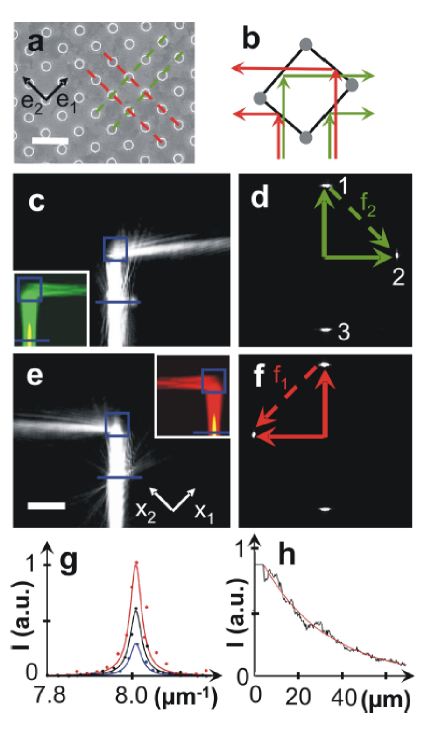
In addition, energy conservation imposes the condition and as a consequence Bragg reflection occurs only for specific angles and wavelengths. This opens a possibility for spectral demultiplexing if we put different Bragg mirrors 1, 2,… in series such that for each mirror Eq. 1 is satisfied at a different SPP wavelengths , ,… . For practical reasons, however, we do not use this configuration here due to the short SPP propagation length m in the visible spectral range. We propose rather a compact solution in which two Bragg mirrors optimized for two different wavelengths are superimposed. Indeed, if nanoscale protrusions (or indentations) are positioned at the intersection points of two sets of Bragg lines with different orientations built to reflect respectively the wavelengths and one obtains a 2D plasmonic crystal presenting optical band gaps around these wavelengths (Figs. 1a,b).
To demonstrate this approach we have investigated a plasmonic crystal demultiplexer optimized for the two SPP wavelengths nm and nm which correspond to laser wavelengths of respectively 800 nm and 750 nm. We fabricated rectangular 2D lattices made of gold protrusions (200 nm diameter, 50 nm height) deposited on a gold film (see Fig. 1a). As sketched in Fig. 1b we expect in such conditions that incoming SPP waves with wavelength and are reflected in two opposite directions. This is indeed what is observed experimentally (compare Fig. 1c and 1e) using leakage radiation microscopy (LRM) which is based on the conversion of SPP waves to propagating light Hecht:1996 ; Bouhelier:2001 ; Stepanov:2005 .
To understand more precisely this effect we must apply Eq. 1 considering the reciprocal vector . The reciprocal lattice basis (i=1,2) is connected to the primitive lattice vector basis (see Fig. 1a) by , where are the lattice periods . Values of nm and nm were chosen in order to realize Bragg reflection. An incident SPP impinging on the crystal in the vertical direction (see Fig. 1a) is thus expected to be reflected to the right (i. e., the direction, see Fig. 1b) or to the left (i. e., the direction, see Fig. 1b) depending on the SPP wavelength or , respectively. SPPs are launched by focussing a laser beam onto a gold ridge Ditlbacher:2002 and propagate subsequently in the directions , as seen in Figs. 1c,e which show the LRM images for the SPP wavelengths and . We observe that the SPP propagating in the direction is efficiently reflected upon interaction with the plasmonic crystal as expected, i.e., to the right for and to the left for (Figs. 1c,e).
Being a far-field optical method LRM enables the imaging and direct quantitative analysis of SPPs in both direct and Fourier space Hecht:1996 ; Drezet:2006 . The Fourier image (i.e., momentum maps) corresponding to Fig. 1c (respectively 1e) is shown in Fig. 1d (respectively 1f) and reveals three distinct spots. The spots labelled 1 and 3 correspond to the SPPs propagating in the and directions, respectively, while the spot labelled 2 corresponds to the reflected SPP (Figs. 1d). Due to energy conservation all three spots 1-3 must be located on a same Ewald circle, as found in the experiment. The transfer of momentum (i. e., at the SPP wavelength ) is directly evident from the images as plotted by the dashed arrows in Figs. 1d,f while incident and reflected SPPs are represented by the continuous arrows.
Furthermore, these data allow the strightforward quantitative analysis of the plasmonic crystal efficiency. For this purpose, we have to take into account the exponential damping of the SPP intensity along the SPP propagation direction. In quantitative terms, the intensities of the three spots 1-3 in Figs. 1d,f are related by the expressions and , where and are the reflection and transmission coefficients of the plasmonic crystal and r=32 is the distance separating the SPP launch ridge from the plasmonic crystal. On the basis of cross-cuts trough the spots 1-3 to retrieve quantitative information from the images (see Fig. 1g) we deduced % and % for the SPP wavelength Drezet:2006 . This implies losses of around 20% which we attribute to out-of-plane scattering. The radial shape of the observed SPP peaks (see Fig. 1g) can be theoretically reproduced by using a Lorentzian fit. This is in agreement with previous studies Burke:1986 ; Drezet:2006 showing that the full-width-at-half-maximum of such peaks are a direct measure of . We found here which is in good agreement with the measurement of the exponential SPP damping in direct space (not shown). Angular cross–cuts of the SPP peaks (see Fig. 1h) show that the angular divergence is conserved when going from 1 to 3. The same analysis for the SPP wavelength yields %, % and %.
To corroborate our results we simulated the interaction of a SPP beam with the plasmonic crystal by using a 2D dipolar model Drezet:2005 . While interparticle coupling was neglected in our model (i. e. we worked in the limit of the first Born approximation) qualitative agreement with the experimental observations for the two considered wavelengths is obtained, see the insets in Figs. 1c,e.
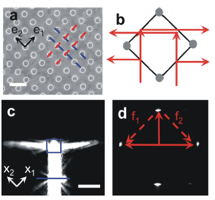
We now turn to the special case (and thus a plasmonic crystal with a quadratic unit cell) which corresponds to a SPP splitter (Figs. 2a,b). We studied this system for a laser wavelength of 750 nm corresponding to a SPP wavelength nm. In the direct space LRM image in Fig. 2c the splitting of the incoming SPP beam is clearly observed. In the Fourier image in Fig. 2d one observes 4 spots corresponding to the two counter–propagating SPPs launched from the gold ridge and to the two reflected SPP beams. This image again illustrates directly how momentum transfer operates in such a device. Quantitative analysis as above indicates that about 80 % of the incoming SPP intensity is reflected equally between SPPs propagating to the right and to the left of the crystal (i. e., in the and directions, respectively). The residual part of the intensity ( %) is again attributed to loss due to scattering.
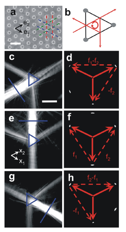
The beam splitting and demultiplexing properties of plasmonic crystals are not restricted to two output beams. For example, choosing a triangular lattice instead of a rectangular one (Fig. 3a) splits an input beam into three output beams. The triangular lattice can be thought of as resulting from the overlap of three Bragg mirrors such that the angle between the corresponding Bragg lines equals . Choosing the distance separating two adjacent parallel Bragg lines such that one obtains Bragg reflection at incidence angle. This corresponds to an interparticle distance in the triangular lattice of . Due to its symmetry such a plasmonic crystal represents a six-port device (three inputs and three outputs) that has been called “tritter” before Zeilinger:1997 . We realized a tritter working at nm, i. e., at 750 nm laser wavelength by placing gold particles with 200 nm diameter and 70 nm height within an area enclosed by an equilateral triangle with m side length. The LRM image in Fig. 3c shows that a SPP beam (incident from the lower left) is indeed split into three reflected beams. The identical results when using the two other inputs are shown in Figs. 3e,g. Again, the directions of the vectors can be taken directly from the Fourier space images in Figs. 3d,f,h which show clearly the four spots corresponding to the incident and the three reflected SPPs. The dashed arrows correspond to a momentum transfer of , , or , depending on the incident beam direction and the output beams considered (compare Figs. 3d,f,h). We find that for the chosen geometry the plasmonic crystal tritter distributes 85% of the incident SPP intensity equally between the three outputs. The remaining % are again attributed to scattering loss.
While all results discussed here were achieved within the visible spectral range, plasmonic crystal devices are expected to perform even better (e.g., in terms of spectral selectivity) in the infrared (telecom) spectral range due to significantly lower ohmic losses Nikolajsen:2003 . In general, the use of multiplexers, splitters and tritters in photonic applications might be specifically appealing due to their small footprint in the range of m2. Furthermore, the use as building blocks for classical Teich or quantum Knill:2001 optical computing can be envisaged.
We acknowledge financial support from the EU under projects FP6 NMP4-CT-2003-505699 and FP6 2002-IST-1-507879.
References
- (1) Joanopoulos, J. D., Villeneuve, P. R., Fan, S., Photonic crystals: putting a new twist on light. Nature 386, 143-149 (1997).
- (2) Smith, D. R. et al., Composite Medium with Simultaneously Negative Permeability and Permittivity . Phys. Rev. Lett84, 4184-4187 (2000).
- (3) Barnes, W. L., Dereux, A., Ebbesen, T. W., Surface plasmon subwavlength optics. Nature 424, 824-830 (2003).
- (4) Genet, C., Ebbesen, T. W., Light in tiny holes. Nature Nature 445, 39-46 (2007).
- (5) Raether, H. Surface Plasmons (Springer, Berlin, 1988).
- (6) H. Ditlbacher, Krenn, J. R., Schider, G., Leitner, A. and Aussenegg, F. R. Two-dimensional optics with surface plasmon polaritons. Appl. Phys. Lett. 81, 1762-1764 (2002).
- (7) Weeber, J.-C., González, M. U., Baudrion, A.-L., and Dereux, A. Surface plasmon routing along right angle bent metal strips. Appl. Phys. Lett. 87, 221101 (2005).
- (8) Stepanov. A et al. Quantitative analysis of surface plasmon interaction with silver nanoparticles. Opt. Lett. 30, 1524-1526 (2005).
- (9) Drezet, A. et al. Surface plasmon propagation in an elliptical corral. Appl. Phys. Lett. 86, 074104 (2005).
- (10) Drezet, A. et al. How to erase surface plasmon fringes. Appl. Phys. Lett. 89, 091117 (2006).
- (11) Baudrion, A. L. et al. Influence of the filling factor on the spectral properties of plasmonic crystals. Phys. Rev. B 74, 125406 (2006).
- (12) Kitson, S. C., Barnes, W. L. and Sambles, J. R. Full Photonic Band Gap for Surface Modes in the Visible. Phys. Rev. Lett. 77, 2670-2673 (1996).
- (13) Bozhevolnyi, S. I. et al. Waveguiding in Surface Plasmon Polariton Band Gap Structures. Phys. Rev. Lett. 86, 3008-3011 (2001).
- (14) Hecht, B. et al. Local Excitation, Scattering, and Interference of Surface Plasmons. Phys. Rev. Lett. 77, 1889-1892 (1996).
- (15) Bouhelier, A. et al. Plasmon optics of structured silver films. Phys. Rev. B 63, 155404 (2001).
- (16) Burke, J. J., Stegeman, G. I. and Tamir,T. Surface-polariton-like waves guided by thin, lossy metal films. Phys. Rev. B 33, 5186-5201 (1986).
- (17) Zukowski, M., Zeilinger, A. and Horne, M. A. Realizable higher-dimensional two-particle entanglements via multiport beam splitters. Phys. Rev. A 55, 2564-2579 (1997)
- (18) Nikolajsen, T. et al. Polymer-based surface-plasmon-polariton stripe waveguides at telecommunication wavelengths. Appl. Phys. Lett. 82, 668-670 (2003).
- (19) Saleh, B. E. A., Teich, M. C. Fundamentals of Photonics (Wiley, New York, 1991).
- (20) Knill, E., Laflamme, R. and Milburn, G. J. A scheme for efficient quantum computation with linear optics. Nature 409, 46-52 (2001).