Thermal shot noise in top-gated single carbon nanotube field effect transistors
Abstract
The high-frequency transconductance and current noise of top-gated single carbon nanotube transistors have been measured and used to investigate hot electron effects in one-dimensional transistors. Results are in good agreement with a theory of 1-dimensional nano-transistor. In particular the prediction of a large transconductance correction to the Johnson-Nyquist thermal noise formula is confirmed experimentally. Experiment shows that nanotube transistors can be used as fast charge detectors for quantum coherent electronics with a resolution of in the – band.
pacs:
73.63.Fg, 72.10.Di, 73.22. fField effect transistors (FETs), such as quantum point contact transistors Gustavsson2008NL , are an alternative to Coulomb blockade devices (SETs)Andresen2008JAP for fast single charge detection in nanostructures due to their smaller impedance. In the perspective of a future quantum electronics based on ballistic electrons Feve2007Science , or the fast readout of charge qubits, a nanosecond time resolution is needed that is challenging but should be reachable by using nano-transistors. A well-known realization is a top gated single carbon nanotube Tans1998Nature , which works at high frequency Chaste2008NanoL (see review in Rutherghen2009NatMat ). Ultimate gate coupling and finite density of states in the channel push these nano-transistors close to the quantum limit where gate capacitance approaches the quantum capacitance Chaste2008NanoL . Beside large charge sensitivity, an important limiting factor of resolution is thermal noise from hot electrons which is prominent in low-dimensional conductors due to poor energy relaxation Pothier1997PRL ; Lazzeri2006PRB . Effect of dissipation can be investigated by measuring the out-of-equilibrium phonon population at finite bias Steiner2009NatureNanotech but also by noise thermometry Wu2007PRB . The nano-transistor geometry offers an opportunity to revisit these hot electron effects using the additional control of electronic transmission.
The noise thermometry approach of electronic population relies on assumption of a thermal distribution and the Johnson-Nyquist formula relates the current noise spectral density to the electronic temperature via a so-called ”noise conductance” van_der_Ziel1962IEEE . In general one has , the differential drain conductance. The situation is different in gated semiconductors where an additional contribution arises, at finite bias, associated with transconductance where is the drain current and the gate voltage. This term depends a priori on geometry, at least for the 3D and 2D transistors van_der_Ziel1962IEEE ; Naveh1999PRB . We show here that the situation is different at 1D and that a simple relation exists between , and which only brings in the gate coupling factor .
The paper reports on current noise and transconductance of top-gated single nanotube transistors. Measurements were carried at 4K to take advantage of the enhanced noise resolution of cryogenic setups and in a GHz bandwidth to overcome the low frequency noise and benefit from the good AC coupling in the contact impedance. Hot electron effects show up both in the thermal current noise and the width of the transconductance peak at the onset of conduction. Using a 1D nano-transistor model based on scattering theory Blanter2000PhysRep we obtain a generalized Johnson-Nyquist noise formula in the form,
| (1) |
where conductance terms and noise are to be taken at the same frequency. Eq.(1) is supported by the RF measurements of transconductance and noise and the electronic temperature reported below as function of bias voltage. As electronic temperature depends on current, one can alternatively express thermal noise as , by introducing a pseudo Fano factor . The limit corresponds to a classical shot noise as observed in vacuum diodes. The hot electron regime shows up in our nanotube transistor by a full thermal shot noise with at low bias followed by some reduction () resulting from Pauli principle and the effect of electronic degeneracy which generally shows up at high bias.
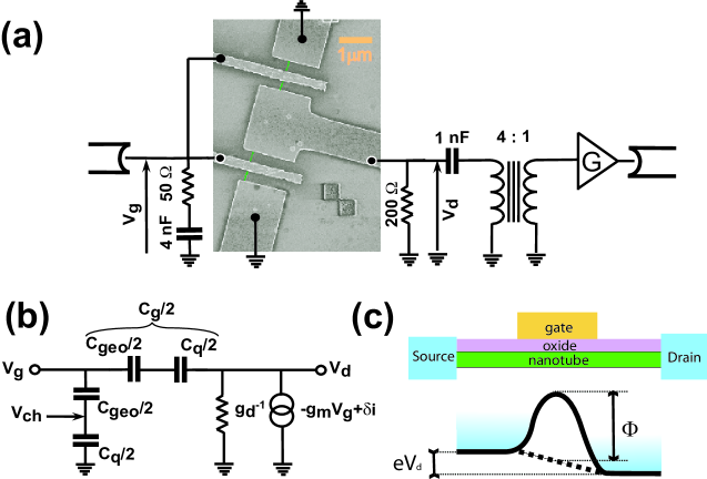
The sample (Fig.1(a)) is taken from a batch which was extensively described and characterized in Ref.Chaste2008NanoL . A symmetric double gate RF design is used (Fig.1(a)) on high resistivity silicon substrate. The high mobility CVD-grown nanotube (diameter ) is equipped with a top gate (length ) deposited on a thin AlOx oxide (thickness ). Palladium drain and source metallisations are used for low Schottky barrier contacts. Our high-sensitivity cryogenic setup includes a low noise amplifier fitted to a – impedance matching transformer with a cutoff. Matched resistors are fitted at the input and output lines to obtain a broad – measuring band. The 200 Ohms output load ensures DC voltage bias conditions and serves as an auxiliary white noise source for in-situ calibration. The lumped circuit element description of the nanotube transistor (Fig.1(b)) is used for RF data analysis and the theoretical model below. The gate capacitance, , is taken from the room temperature RF probe station measurements Chaste2008NanoL . With () we deduce Chaste2008NanoL . We have used negative drain bias, which shows lower noise and symmetric gate bias conditions. and are taken by reference to the pinch-off value (at ).
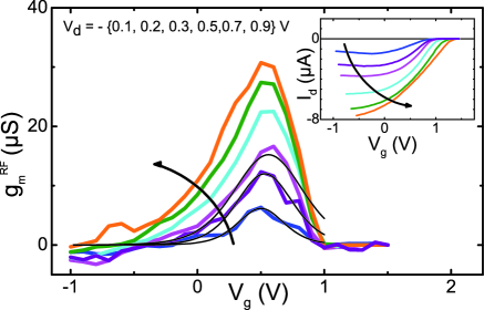
Figure 2 shows the radio frequency transconductance deduced from transmission measurements Chaste2008NanoL as function of gate voltage for different bias conditions. The DC conductance and transconductance are obtained from the characteristics (Fig.2-inset). Reflection coefficients, and , cannot be accessed with this setup. The sample shows large , typically 3-times larger than , which suggests AC contact coupling. We observe a small temperature dependence of (a decrease between 4K and 300K) which we take as a first indication of a hot electron regime.
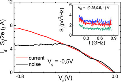
In Fig.3 we discuss measurements of the transistor in the open state () where . Here the nanotube behaves as a metallic wire with a finite transmission , deduced from low bias current and presumably limited by contact barriers. As seen in the figure, a full shot noise limit is observed for , followed by a saturation plateau. Although the noise characterization is certainly relevant for understanding the saturation mechanism that takes place in nanotubes at very high bias, we prefer to leave this discussion for a future work. Using ( and in Eq.(1)) we deduce and an (over-) estimate of electronic temperature . Indeed, this ratio is larger than a theoretical expectation, , for a Wiedemann-Franz resistance limited thermal sink Kumar1996PRL . Importantly, both numbers show that a hot electron regime is expected and present in the nanotube. As discussed below, we can rely on the transconductance characteristics for an independent determination of the electronic temperature of the nanotube working as a transistor.
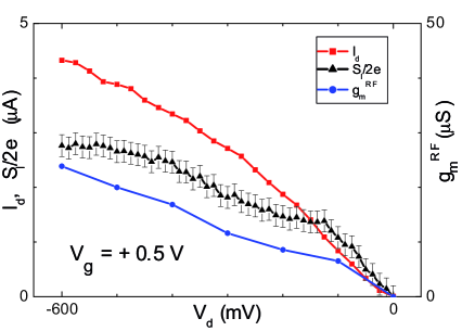
Fig.4 contains the main experimental results of the paper, namely the bias dependence of , and , at the transconductance maximum (). The dependence is similar to that observed in the open state with, as a difference, a first noise plateau () observed in range –. The two step increase of noise and the width of the plateau () are suggestive of the subband structure of the nanotube (intersubband-gap – for a diameter). In order to secure 1D transport conditions, we shall therefore focus below to the () bias range.
For the theoretical analysis we rely on a simple 1D nano-transistor model. The nanotube is described as a fourfold degenerate 1D channel decomposed in three sections (see Fig.1(c)): a central part covered by the top-gate which acts as a local classical barrier and two ungated nanotube leads on both sides which constitute the drain and source reservoirs of the transistor. The leads are diffusive and assumed to be populated with Fermi distributions and . The barrier (height ) acts as an high-pass energy filter with quasi-ballistic high energy electrons (transmission for ) and reflected low energy ones ( for ). With these assumptions and scattering theory Blanter2000PhysRep one can readily calculate current and noise to deduce the differential conductance , the transconductance
| (2) |
and the noise conductance . According to the equivalent circuit in Fig.1(b), we have taken . These three ”conductances” depend on two parameters, the drain and source occupation numbers (at ), and therefore obey the constitutive relation which gives rise to Eq.(1). Details of screening, which are encoded in the functional, or temperature in , are implicit in Eq.(1) which can be regarded as a universal result for 1D transistors. In terms of thermal shot-noise one has (for ) at low bias where . At high bias one has whenever ; one also expect Pauli noise suppression with a reduction factor like in the usual 2D case Naveh1999PRB .
As a first test of the model we obtain a good fit of the data in Fig.2 with Eq.(2) by taking and in according to the equivalent circuit and the potential landscape in Figs.1(b) and (c). We have used a scaling factor that accounts for residual electronic diffusion above the barrier. Electronic temperatures deduced from theoretical fits corresponds to a large absolute temperature ( at ), but still a small energy spread when compared to the bias voltage () .
The model accounts qualitatively for a full shot-noise at low bias ( for ) and for the noise reduction at intermediate bias (–). Using the electronic temperature from transconductance fits in Fig.2, we can quantitatively compare noise and transconductance in Eq.(1): At , where , and we obtain in good agreement with theoretical prediction from Eq.(1). By comparison standard noise thermometry would give a smaller value (taking ). We take this agreement as a strong support for the 1D model. Further experimental investigations should involve direct measurement of to test Eq.(1) over the full bias range including the crossover .
Finally we can use our data to estimate the charge resolution . The best signal to noise conditions, for and where and , give ( Chaste2008NanoL ) for our double gate device which corresponds to an rms charge resolution of 0.4 electron in the bandwidth of our set-up. Within a factor five of the best resolution achieved in SETs Andresen2008JAP , this smaller sensitivity of the present CNT-FETs is balanced by a much larger bandwidth ( here against in Andresen2008JAP ) and the possibility to operate at room temperature.
In conclusion, our comprehensive study of high-frequency transport and shot noise has confirmed that the single nanotube transistor is a model system and that hot electron effects are prominent at 1D. In particular our data support a generalized Johnson-Nyquist expression for thermal noise in 1D transistors introduced in the paper. Finally we have benchmarked nanotube FETs against nanotube SETs for applications as fast single electron detectors.
Acknowledgements.
Authors acknowledge fruitful discussions with G. Dambrine, V. Derycke, P. Dollfus, C. Glattli, H. Happy and M. Sanquer. The research has been supported by french ANR under contracts ANR-2005-055-HF-CNT, ANR-05-NANO-010-01-NL-SBPC, and EU-STREP project CARDEQ under contract IST-FP6-011285.References
- (1) S. Gustavsson, R. Leturcq, T. Ihn, M. Studer, K. Ensslin, D.C. Driscoll, and A.C. Gossard, Nano Lett. 8, 2547 (2006).
- (2) S. E. S. Andresen, F. Wu, R. Danneau, D. Gunnarsson and P. J. Hakonen, J. Appl. Phys 104, 033715 (2008).
- (3) G. Fève, A. Mahé, B. Plaçais, J.-M. Berroir, T. Kontos, A. Cavanna, Y. Jin, B. Etienne and D. C. Glattli Science 316, 1169 (2007).
- (4) S.J. Tans, A.R.M. Verschueren, and C. Dekker, Nature 393, 49 (1998)
- (5) J. Chaste, L. Lechner, P. Morfin, G. Fève, T. Kontos, J.-M. Berroir, D. C. Glattli, H. Happy, P. Hakonen, B. Plaçais, Nano Lett. 8, 525 (2008)
- (6) C. Rutherghen, D. Jain P. Burke, Nature Nanotech.. 4, 911 (2009).
- (7) H. Pothier, S. Gueron, N.O. Birge, D. Esteve, M.H. Devoret, Phys. Rev. Lett. 779, 3490 (1997).
- (8) M. Lazzeri, F. Mauri, Phys. Rev. B 73, 165419 (2006).
- (9) M. Steiner, M. Freitag, V. Perebeinos, J. C. Tsang, J. P. Small, M. Kinoshita, D. Yuan, J. Liu, P. Avouris, Nature Nanotech. 4 , 320 (2009).
- (10) F. Wu, T. Tsuneta, R. Tarkiainen, D. Gunnarsson, T.H. Wang, and P.J. Hakonen , Phys. Rev. B 75, 125419 (2007).
- (11) A. van der Ziel, Proc. IRE 50, 1808 (1962).
- (12) Y. Naveh, A.N. Korotkov, and K.K. Likharev, Phys. Rev. B 60, 2169 (1999).
- (13) Y.M. Blanter, M. Büttiker, Phys. Rep. 336, 1 (2000)
- (14) A. Kumar, L. Saminadayar, D. C. Glattli, Y. Jin and B. Etienne, Phys. Rev. Lett. 76, 2778 (1996).