Effective-mass model of surface scattering in locally oxidized Si nanowires
Abstract
We present a simple model to describe the lowest-subbands surface scattering in locally oxidized silicon nanowires grown in the [110] direction. To this end, we employ an atomistically scaled effective mass model projected from a three-dimensional effective mass equation and apply a quantum transport formalism to calculate the conductance for typical potential profiles. Comparison of our results with hole-transport calculations using atomistic models in conjuction with Density Functional Theory (DFT) points to an intra-subband scattering mechanism from a potential well.
Index Terms:
Intraband scattering, silicon nanowires, oxidationtoday
I Introduction
Recent bottom-up [1] and top-down [2, 3] demonstrations of Si channels with diameters of only a few nanometers shape the roadmap towards the ultimate limits of scaling. Silicon nanowires (SiNWs), in particular, can be easily integrated with existing semiconductor technologies. As experimental results remain difficult to obtain and analyze at this lengthscale, modelling has a crucial role to play in assessing this technology.
Owing to computational and methodological advances, great progress has been achieved in atomic-scale transport calculations, first in molecular systems [4, 5] and later in semiconductor nanowires [6, 7, 8, 9]. Nevertheless, semiconductor physics is most easily captured within the effective mass theory and many device simulators are built based on this approximation [10, 11]. This implies that simple models describing the basic mechanisms are required [12]. Recently, using an effective mass model we were able to determine the important parameters in scattering from neutral P-dopants in SiNWs and reproduce results from a first-principles approach within DFT [13].
Here, in a similar fashion, we take a first step in explaining scattering from Si atoms at the wire surface promoted to different oxidation states (typically Si+1 and Si+2). Due to oxidation, this type of oxygen-related defects are unavoidable at the surface of a pure semiconductor wire core even in surface treated SiNWs and can be considered as a source of roughness on the atomic scale [8, 14]. Using an effectively one-dimensional model of scattering from a well we fit the conductance of ultrathin ( 3nm in diameter) SiNWs as obtained from a combined DFT-Green’s function formalism. An atomic-scale analysis based on calculations from first-principles will be presented elsewhere [9]. This approach allows us to identify the scattering mechanism as intra-subband scattering from a shallow potential well.
In Section II, we summarize the equations of the effective mass model solved using a quantum transport scattering approach. In Section III, we present a discussion of our results for various typical scenarios of local surface oxidation. We conclude with Section IV.
II Effective mass equations
The general Hamiltonian that governs the three-dimensional electron motion reads
| (1) |
Here, is the effective mass tensor in the coordinate system of the device (i.e., x-axis is oriented along the channel) , is the momentum operator for a fully spatially quantized electron motion and is the single-particle operator for the electrostatic potential that the electron feels when injected in the channel. In what follows we focus on hole transport and take that the effective mass tensor is diagonal within our SiNW coordinate system. This leads to an effective mass Hamiltonian 1 for the nanostructure reading [15]
| (2) |
We also assume that the effective mass varies only along the channel, i.e., the x-direction, allowing us to use an ansatz of the form
| (3) |
Applying this ansatz and using the orthonormality property for the function together with a ’smooth disorder’ assumption along transport, i.e. very slow variation, then it is eligible to assume that the function is independent of . This approximation has also been used in Ref. [16]. Under these assumptions we end up with an one-dimensional effective mass equation governing transport within the nanowire
| (4) |
where is determined by the solution of
| (5) | |||
The quantum mechanical scattering problem corresponding to Equation 4 is then solved to yield the transmission coefficient, , for each channel and, hence, the Landauer conductance .
III Results
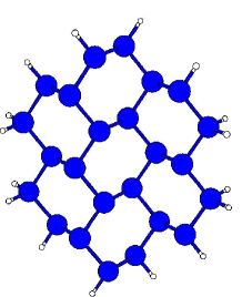
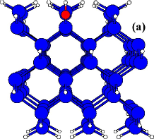
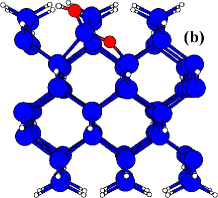
For definitiveness, we consider SiNWs grown along the [110]-direction and fix the diameter to nm. Similar results are obtained for the lowest subbands in wires with larger W. Figure 1 shows the cross-section of the wire channel. The atomistic model for the promotion of Si atoms to the states Si+1 and Si+2 consists of starting from the neutral oxidation state Si0 at the surface of the hydrogenated wires and introducing oxygens as shown in Figure 2. The resulting Si-O-H and Si-O-Si bonds are the simplest cases of oxygen bridge- and back- bonds.
Before performing a transport calculation using Eq. 4 it is instructive to compare the electronic structure of the pristine hydrogenated wire with the bands of a large enough supercell that includes an oxygen-derived defect. This is done in Figure 3, where we plot the bands derived from a density functional tight-binding (DFTB) approach. The latter is an efficient approximation to the Kohn-Sham DFT scheme. We first note that the effective mass as determined by the curvature of the bands does not change by the introduction of the oxygen. In general, impurities cause variations of the effective mass along the channel. But here this effect can be disregarded.
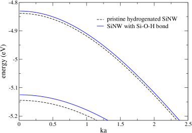
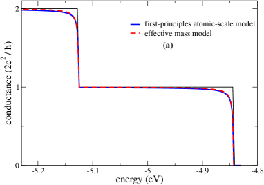
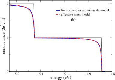
A second observation is that alignment of the bands in a pristine-oxidised-pristine wire arrangement would yield a potential well of the order of a few meV for hole propagation in both subbands. For the effective mass model, we take this into account as a phenomenological parameter in Eq. 4 through the x-dependence of W. The conductance for a potential well extending over a region of length is plotted in Figure 4. Also in Figure 4, we show for comparison the result of a combined DFTB-Green’s function approach as well as the ideal hole conductance of a pristine hydrogenated wire. It is evident that for both cases of an Si-O-H bond and an Si-O-Si back-bond the simple model of considering the region around the oxidized Si site as a shallow potential well yields a remarkable quantitative agreement. This picture is consistent with ballistic transport and the positive oxidation state of Si. We note that within the effective mass model only intrasubband scattering is considered, thereby, implying that this is the dominant scattering mechanism. As an aside we confirmed this by independent analysis of the quantum mechanical S-matrix in the atomic-scale model.
IV Conclusion
In conclusion, effective mass models are useful in analyzing measurements, model building and for practical calculations of charge carrier transport in semiconductor wires. To this end, we derived a simple picture within this framework to explain results of hole-transport calculations in locally oxidized silicon nanowires grown in the [110] direction using atomic-scale models in conjuction with Density Functional Theory (DFT). This appoach points to an intra-subband scattering mechanism from a potential well and may further apply in other impurity systems.
Acknowledgment
P. Drouvelis acknowledges financial support from the Irish Research Council for Science Engineering and Technology while at Tyndall National Institute where part of this work was performed. The research of G. Fagas is supported by Science Foundation Ireland.
References
- [1] C. Yang, C. J. Barrelet, F. Capasso, and C. M. Lieber, Nano Lett. 6, 2929 2006.
- [2] C. P. Lansbergen, R. Rahman, C. J. Wellard et al, Nat. Phys. 4, 656 (2008).
- [3] J.-P. Colinge(ed), FinFETs and Other Multi-Gate Transistors (Springer, 2007).
- [4] G Cuniberti, G Fagas and K Richter(eds), Introducing Molecular Electronics, (Springer, 2005)
- [5] S. Datta, Quantum Transport Atom to Transistor (Cambridge University Press, 2005).
- [6] Y. Zheng, R. Lake, K. Alam, T. B. Boykin, G. Klimeck, Electronic properties of silicon nanowires, IEEE Trans. Elec. Dev. 52, 1097 (2005).
- [7] N. Neophytou, A. Paul, M. S. Lundstrom, and G. Klimeck, IEEE Trans. Elec. Dev. 55, 1286 (2008).
- [8] M. Luisier, A. Schenk, and W. Fichtner, Appl. Phys. Lett. 90, 102103, (2007)
- [9] G. Fagas and J. Greer (submitted)
- [10] S. Roy and A. Asenov, Science 309, 388 (2005).
- [11] D. Vasileska, D. Mamaluy, H. R. Khan, K. Raleva, and S. M. Goodnick, J. Comput. Theor. Nanosci. 5, 999 (2008).
- [12] N. Neophythou, A. Paul, M. S. Lundstrom, G. Klimeck, J. Comput. Electron. 7, 363 (2008).
- [13] P. Drouvelis and G. Fagas (submitted)
- [14] M. H. Evans, X.-G. Zhang, J. D. Joannopoulos, and S. T. Pantelides, Phys. Rev. Lett. 95, 106802 (2005)
- [15] A. Rahman, M. S. Lunstrom, A. W. Gosh, J. Appl. Phys. 97, 053702 (2005).
- [16] J.Wang, E. Polizzi, M. Lundstrom, J. Appl. Phys. 96, 2192 (2004).