Engineering Time-Reversal Invariant Topological Insulators With Ultra-Cold Atoms
Topological insulators are a broad class of unconventional materials that are insulating in the interior but conduct along the edges. This edge transport is topologically protected and dissipationless. Until recently, all existing topological insulators, known as quantum Hall states, violated time-reversal symmetry. However, the discovery of the quantum spin Hall effect demonstrated the existence of novel topological states not rooted in time-reversal violations. Here, we lay out an experiment to realize time-reversal topological insulators in ultra-cold atomic gases subjected to synthetic gauge fields in the near-field of an atom-chip. In particular, we introduce a feasible scheme to engineer sharp boundaries where the “edge states” are localized. Besides, this multi-band system has a large parameter space exhibiting a variety of quantum phase transitions between topological and normal insulating phases. Due to their unprecedented controllability, cold-atom systems are ideally suited to realize topological states of matter and drive the development of topological quantum computing.
I Introduction
The search of exotic states of matter has been one of the key driving elements of condensed-matter physics. Among these unconventional phases, the quantum Hall effect has been the paradigm of topological phases not captured by Landau symmetry breaking. Recently, the subject of topological insulators has emerged as a new frontier, discovering novelties in the single-particle band theory and providing a new impetus to the constantly evolving quantum many-body physics of strongly correlated systems HasanKane . The topological classication of insulators and superconductors points towards an inherent universality underlying these exotic states of matter Kitaev .
A new kind of topological insulator, based on the quantum spin Hall (QSH) effect Kane2006 , was first theoretically predicted Kane2005bis ; Bernevig2006 ; Bernevig2006bis ; Fu2007 , then experimentally confirmed in HgTe/CdTe quantum wells Konig2007 and three-dimensional Bi2Te3 Chen2009b . Unlike quantum Hall effects, both integer Klitzing1980 (IQHE) and fractional Tsui1982 , the QSH effect occurs at zero magnetic field and thus respects time-reversal (TR) symmetry. The simplest model of the QSH effect consists of non-interacting charged spin-1/2 fermions where the two spin components are described as IQHE states at equal but opposite “magnetic fields.” This composite system produces degenerate (Kramers) pairs of counter-propagating chiral edge states with opposite spins. Residing in the bulk gap of the band structure, edge modes are gapless excitations that provide the backbone for the topological classification of the insulators. In contrast to the usual IQHE where edge states carry electrical current with quantized conductance Hatsugai1993 , the edge states in QSH systems carry robust spin currents. In the ideal model, the latter are associated to a quantized spin-conductivity Kane2005 ; Bernevig2006 .
In electronic materials QSH effects result from spin-orbit (S-O) coupling, and spin-mixing interactions destroy the quantization of the spin Hall conductivity. A simple way to determine the fate of QSH insulators upon spin mixing is to count the number of Kramers edge pairs inside the bulk gap. Due to TR symmetry, perturbations can only mix different Kramers pairs and gapless edge states are protected when their number is odd. This signals a QSH insulator whose properties are topologically different from a normal band-insulator (NI) that presents an even number of edge states edge ; edgebis . Therefore, a even/odd topological index captures the distinction between QSH and NI quantum phases. The discovery of topological QSH systems has opened the possibility to design new spintronic devices exploiting the spin-dependent direction of edge or surface states in order to manipulate and transport spin current without dissipation.
Here, we propose an optical-lattice realization Lewenstein2007 ; Bloch2008 of such quantum phases and show that cold atoms provide a simple system where quantum spin-Hall physics can be investigated. The origin of these QSH phases is rooted in engineered gauge fields Lin2009 ; Lin2009bis rather than S-O coupling. We describe an original scheme to synthesize gauge fields, exempt from spontaneous emission implicit in all previous proposals Jaksch2003 ; mueller ; Sorensen2004 ; spielman ; Gerbier2009 ; Osterloh2005 ; Ruseckas2005 . The great versatility offered by cold atom experiments allows us to reach the purest realization of the QSH effect and to explore striking aspects of this topological state of matter. Besides, the non-interacting limit – the ideal realization of QSH phases – and the stability of the topological phases can be explored by means of Feschbach resonances and engineered disorder maciejarxiv .
II The system
Realizing topological insulators with cold atoms is particularly attractive Stanescu2009 ; Stanescuarxiv , and we hereby provide a concrete setup using fermionic 6Li subjected to synthetic gauge fields. There are numerous proposals for creating Abelian Jaksch2003 ; mueller ; Sorensen2004 ; spielman ; Gerbier2009 and non-Abelian Osterloh2005 ; Ruseckas2005 gauge fields, leading to interesting phenomena Goldman2009 ; Goldman2009bis ; Satija1 ; Satija2 ; Zhu2006 ; oh . The vast majority of these proposals depend on laser-induced Raman coupling between internal atomic states; such a method was recently implemented with bosonic 87Rb atoms creating an Abelian gauge field Lin2009 ; Lin2009bis . For the alkali atoms, the requisite coupling limits the possible detuning of the Raman laser beams from the ground S to first excited P transition, about to the excited state fine-structure splitting [ for 87Rb, for 40K, and only for 6Li]. The very small detunings possible for fermionic atoms – 40K and 6Li – imply large spontaneous emission rates and thus the desired gauge fields must be synthesized through an alternate scheme. Here we describe such a setup that combines state-independent optical potentials, with micron scale state-dependent magnetic potentials in an atom chip. Our discussion focuses on harmonically trapped quantum degenerate systems about above the atom chip’s surface. Figure 1 depicts how the required potentials for this proposal can be realized using a combination of static and radio-frequency magnetic fields. By completely eliminating spontaneous emission, this approach makes practical the realization of gauge fields for all alkali atoms.
Our proposal for realizing a fermionic model with a SU(2) gauge structure requires four atomic states , , , and [see Fig. 1 (a)], which are confined in a square optical lattice and described by the Hamiltonian
| (1) |
is a 2-component field operator defined on a lattice site , is the lattice spacing, are integers, and is the nearest-neighbor hopping. In this model the matrices modify the hopping along the -directions and result from the synthetic gauge field [cf. below and Methods]. Here, all the states experience a primary lattice potential along which gives rise to a hopping amplitude kHz. A secondary much weaker lattice slightly staggers the primary lattice with . These lattices, with an approximate period of , are produced by two pairs of lasers, slightly detuned from each other and incident on the reflective surface of the atom chip [see. Fig 1 (b)]. Additionally, these beams create a lattice along with a period, confining the fermions to a 2D plane.
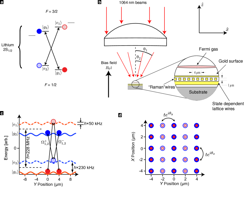
We propose to design the SU(2) hopping operators as follows
| (2) |
where we have set the units , and are Pauli matrices. In order to engineer these state-dependent tunnelings, the states and must experience oppositely-signed lattices realized along the direction of the chip, as in Fig. 1 (c). This scheme exploits the Zeeman shift of an array of wires with alternating currents . The hopping operator in Eq. (2) involves -dependent phases that can be realized with an additional grid of wires spaced by along [cf. Methods]. Remarkably, these moving Zeeman lattices reproduce the Raman-assisted hopping from previous schemes Jaksch2003 ; mueller ; Sorensen2004 ; spielman ; Gerbier2009 and lead to the operator . A potential gradient along detunes this Raman coupling into resonance and is produced by simply shifting the center of the harmonic potential – equivalent to adding a linear gradient. The specific form of the hopping operator is motivated by the fact that it corresponds to opposite “magnetic fluxes” for each spin component, where and are mutually prime numbers. Finally, the additional contribution to the hopping that mixes the and states can be realized in a like manner. The corresponding control parameter , and the additional staggered potential which induces alternate on-site energies along the -axis, are shown below to enrich the phase transitions in a novel manner. Let us emphasize that the Hamiltonian (1)-(2) satisfies Time-Reversal invariance, since it commutes with the TR-operator defined as , where is the complex-conjugate operator. This fundamental symmetry opens the possibility to realize the first instance of -topological insulators in a cold-atom laboratory. Finally, we stress that the two components of the field operators correspond in general to a pseudo-spin 1/2, but in our proposal refer specifically to spin components of 6Li in its electronic ground state.
In this paper, we present results for the case , namely when the synthetic gauge field (2) corresponds to . This choice exhibits an extremely rich phase diagram with almost all possible topological phase transitions [cf. Figs. 4]. The topological phases discussed below are robust against small variations : indeed the properties rely on the existence of bulk gaps which are continuously deformed when is varied, as in the Hofstadter butterfly Hofstadter1976 . Moreover, other configurations of the gauge field could be experimentally designed and would lead to similar effects. In Sect. III, we investigate the phase transitions between topological insulators for a cylinder geometry in the absence of the confining potential . We then show in Sect. IV how these properties can be detected when this confinement is applied.
III Topological insulators and phase transitions
When , Eqs. (1)-(2) describe two uncoupled quantum Hall systems. For generic , the fermion band-structure splits into subbands, the lattice analogues of Landau levels. These subbands are separated by gaps, or by “pseudogaps” exhibiting nodal Dirac fermions. Our setup thus provides a multi-band system, where a variety of band-insulators, separated by metal or semi-metal regions, can be reached by varying the atomic filling factor. As discussed below, some of these insulators are topologically non-trivial and feature gapless edge states. The latter are localized at the boundaries of the sample, and correspond to gapless excitations. When the Fermi energy lies inside a bulk gap, the presence of these states is responsible for the spin transport along the edges.
Figure 2 (a) illustrates the energy spectrum obtained for a cylindrical geometry [cf. Methods]. In this figure, the bulk bands [thick blue bands] are clearly differentiated from the gapless edge states within the bulk gaps [thin purple lines]. In the lowest bulk gap, the edge state channel A, and its TR-conjugate B, correspond to localized excitations which travel in opposite directions [cf. Fig.2 (b)]. Each boundary is populated by a single pair of counter-propagating states, each corresponding to an opposite spin [i.e. helical edge states]. Accordingly, this lowest bulk gap describes a topological QSH phase. Conversely, the next gap located at is traversed by an even number of Kramers pairs, thus yielding a normal band insulator. Remarkably enough, different topological insulators can be experimentally engineered in this multi-band scenario by simply varying the atomic filling factor. The Fermi surface at half-filling, namely , corresponds to a discrete set of isolated points, and thus describes a semi-metal phase.
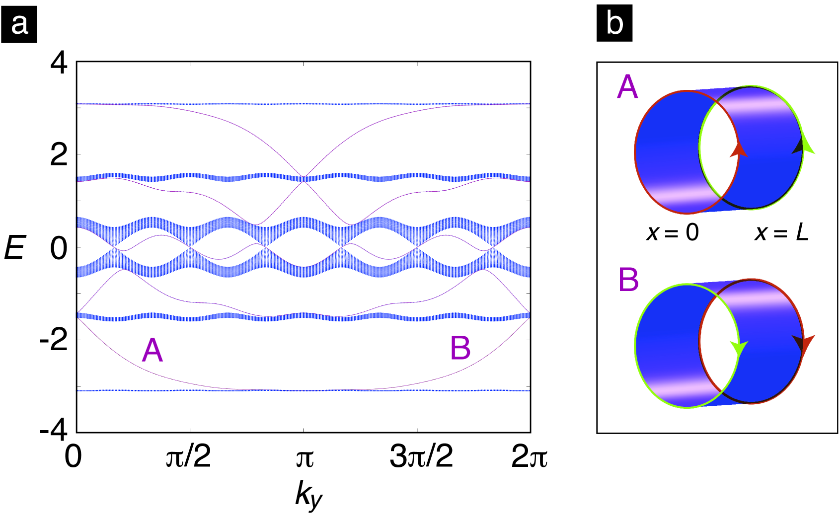
An alternative approach to the above even-odd criteria relies on the computation of a topological invariant that characterizes the bulk gaps [see Methods]. The QSH phase is distinguished from the normal insulator by the index , which respectively takes the value and . We computed this index inside the four gaps depicted in Fig.2 (a), obtaining the following sequence
in perfect agreement with the above edge-state analysis. Therefore, in the uncoupled case where spin is a good quantum number, the spin conductivity is quantized as and is related to the spin current . Additionally, this quantized spin Hall conductivity is equal to the difference of the Chern numbers associated to the up- and down-spin [cf. Methods].
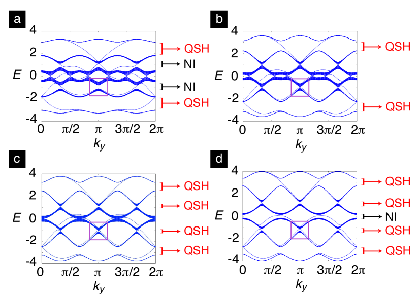
In our multi-band system, the lattice-potential distortions can drive direct transitions between normal and topological insulating states. Figure 3 shows the bulk gaps and edge states for increasing values of the staggered potential’s strength . In the simple case , where two quantum Hall systems are superimposed, we already obtain various realizations of QSH phases. By tuning , one can observe a NI to semi-metal transition, and more importantly, a semi-metal to QSH phase transition in the bulk gaps located around . Remarkably enough, we have shown that the staggered potential, which can be controlled in an optical-lattice experiment, induces a quantum phase transition from a NI to a QSH phase at the critical value [cf. Fig. 3 (b)]. At half-filling, the existence of Dirac points appear to resist the opening of the gap for small staggered potential and eventually lead to a NI phase for [cf. Fig. 3 (d)]. As we describe below, the latter situation radically changes as the coupling is switched on.
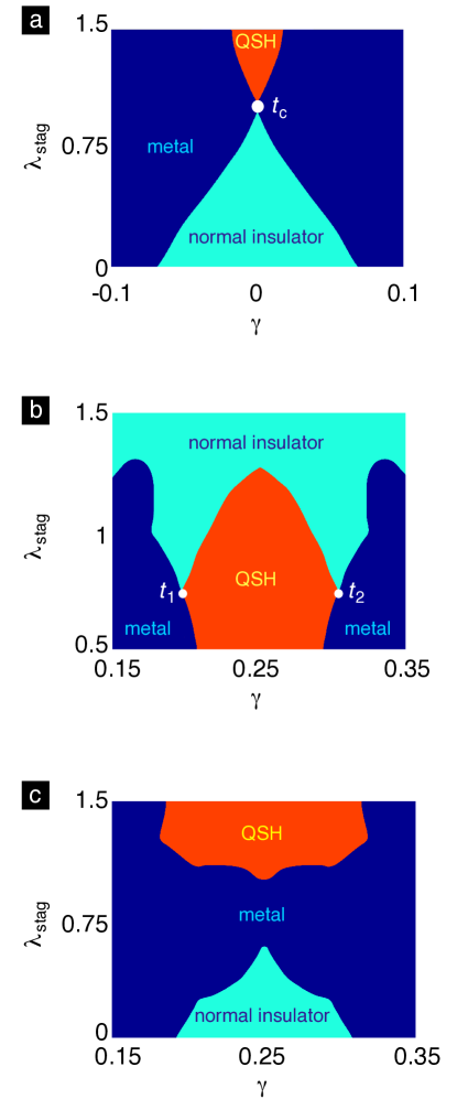
The parameter perturbs the ideal quantum spin Hall system and fundamentally changes the aforementioned phase transitions. The invariant analysis provides a particularly useful and efficient tool to obtain the full phase diagram of the system in the parameters plane [cf. Methods]. The phase diagram represented in Fig. 4(a) has been obtained numerically by evaluating the index inside the bulk at in the vicinity of . Here we observe three distinct regions, namely the metallic (blue), QSH (red), and NI (cyan) phases. These three phases coexist at a tricritical point situated at and . It is interesting to highlight that the QSH phase occurs for a wide range of the parameter , which indicates the robustness of this topological phase under small local perturbations of the Hamiltonian (1).
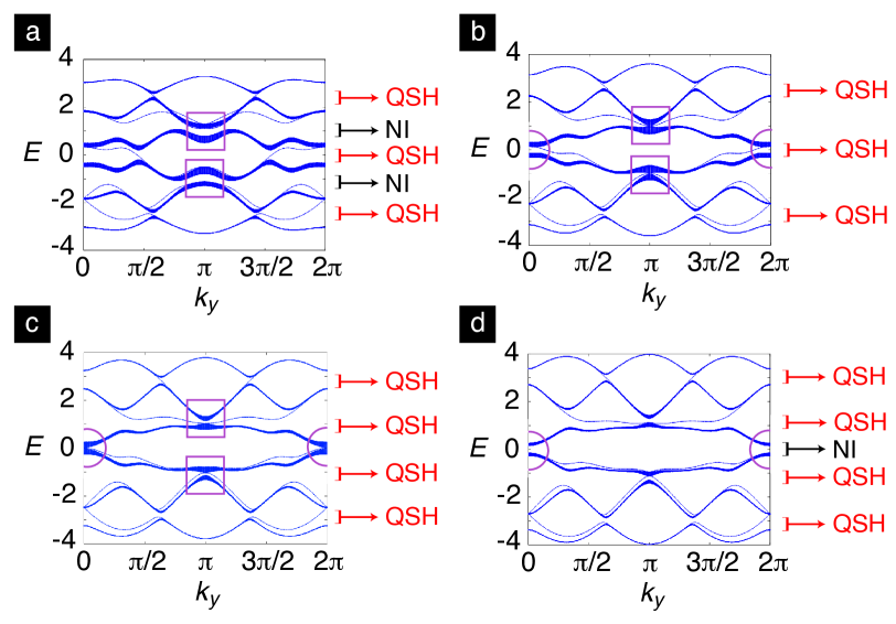
The wide range of possibilities offered by optical-lattice experiments enables us to consider the strong coupling regime corresponding to . In this limit, the previously independent quantum Hall subsystems () become maximally coupled, a fact that drastically modifies the topological phase transitions presented above. In Fig. 5, we illustrate the bulk bands and edge states for increasing values of the staggered potential. Each gap is associated to a QSH or a NI phase according to the even-odd number of TR pairs. In this strong-coupled regime, we observe a completely different phase transition associated to the bulk gap at half filling. Contrary to the semi-metal to NI phase transition described in the uncoupled case [cf. Figs. 3(a)-(d)], we identify here a QSH to NI transition which occurs after a gap-closing at . This process is emphasized on the figures with purple circles [cf. Figs. 5 (b)-(d)]. The QSH phase can only occur at half-filling for large couplings . Furthermore, one also notices that the neighboring bulk gaps at present exactly the opposite phase transition, from a NI to a QSH phase. The latter occurs at , as emphasized on the successive figures with purple rectangles [cf. Figs. 5 (a)-(c)]. Both Figs. 3 and 5 show that the parameters and play competing roles: tends to shrink the gaps width, while tends to open them. In this multi-band configuration, an opening of one of the gaps may result in a gap-closing of the neighboring bands. Therefore, by manipulating the coupling between the states, the staggered potential and the Fermi energy, the system discussed here offers the possibility to explore different topological phase transitions within the several bulk gaps. These novel features endow the topological phase diagram with an intrinsic richness and complexity, not present in other condensed-matter realizations of the QSH effect.
In our model, topological phase transitions of different nature can exist in each of the bulk gaps. As shown in Fig. 5, neighboring bulk gaps can undergo reverse transitions successively. To fully capture the richness of this phenomenon, we numerically compute the index for a wide range of the parameters around . Figure 4(b)-(c) show the bulk gaps at and , respectively. In Fig. 4(b), the central gap features tri-critical points, and the QSH-NI phase transitions occur along a well-defined curve. On the other hand, in the neighboring gap [Fig. 4(c)], the QSH to NI phase transition is separated by an intermediate metallic region. Therefore, we conclude that a single realization of this model allows us to study a wide variety of different topological phase transitions.
IV Detection in the presence of the confining potential
IV.1 The harmonic trap and gauge fields with anisotropic hopping
We now describe a new feasible scheme to engineer a sharp interface where edge states can be localized. This is essential for detecting topological states in optical lattices, where the indispensable harmonic trap used to confine atoms strongly influences the edge states Stanescu2009 ; Stanescuarxiv when , where is the gap’s width. In the present context , requiring temperatures nK.
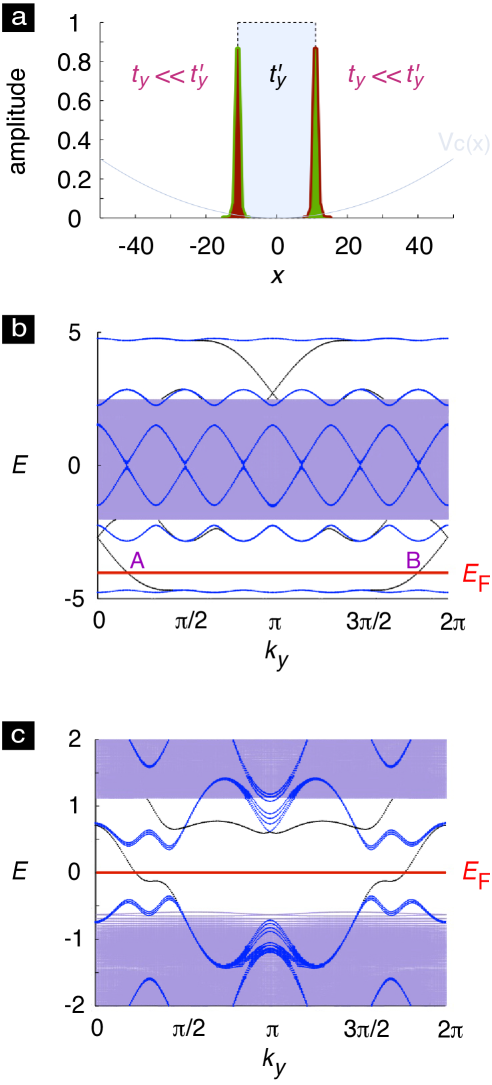
The key aspect of our proposal exploits the fact that the hopping along the -direction, , is laser-controlled and hence can be tuned. Furthermore, since the harmonic trap has a minimal effect at the center of the trap, we divide the chip into three regions: the central region is characterized by a large hopping , while the two surrounding regions feature small hoppings . This highly anisotropic hopping creates a sharp interface where the edge states of the central region – a topological insulator – localize. In other words, by controlling the strength of the Raman coupling, we squeeze the energy bands describing the outer parts so that it does not interfere with the bulk gaps of the central topological phase where the edge states reside. We show that the helical edge states are robust and exactly localized at the interface between the inner and outer regions, whose location can be easily controlled in this scheme [cf. Fig. 6 (a)]. Furthermore, since the topological phases are confined in the center of the trap, one verifies that the phase diagrams discussed in the previous sections are valid for a much wider range of the harmonic potential’s strength. These observations are illustrated in Fig. 6, where the energy spectrum and edge-state wave-functions are depicted for different configurations. In Fig. 6 (b), we observe a new metallic continuum band corresponding to the outer region, which corrupts all but the lowest and highest band gaps. When the Fermi energy lies in the preserved gap, we see how the edge states are robustly localized within the interface [cf. Fig. 6 (a)]. Moreover, Fig. 6 (c) shows that the staggered potential opens a bulk gap at half-filling, allowing to explore the phase diagrams of Fig. 4 (b)-(c).
IV.2 Detecting the edge states and the quantum spin Hall effect
Probing the topological edge states in a cold-atom experiment remains a fundamental challenge Stanescu2009 ; Stanescuarxiv ; Liu2010 . Although density measurements might already detect the accumulation of atoms at the designed edges [i.e., the aforementioned interfaces], alternate techniques should access more profound properties associated to these specific states. For instance, stimulated Raman spectroscopy techniques can measure the dispersion relation of these excitations Dao2007 . A further promising possibility would be to exploit light Bragg scattering in order to observe signatures in the dynamical structure factor Stamper1999 : whenever the Fermi energy crosses a gapless edge-state, a delta peak is distinctively observed in the structure factor Liu2010 . The present proposal is particular suited for testing the latter detection method, since the light scattering can be focused on the interfaces where the edge-states have been shown to be robust in the presence of a confining harmonic potential.
Finally, supplementary signatures of the quantum spin Hall effect could be detected through spin-resolved density measurements Zhu2006 . A synthetic electric field [e.g. by accelerating the lattice or using gravity], should separate the different spin-components, thus detecting spin-currents in the transverse direction. In the case, the spin-Chern number is given by SChN= [see Methods], which can be evaluated through the Streda formula applied to the spin-up density Umucalilar2008 .
V Conclusions and Outlook
In this article, we described a concrete and promising proposal of synthetic gauge fields in square optical lattices that overcomes the severe drawbacks affecting earlier schemes. Moreover, we showed how such engineered gauge fields are ideally suited to experimentally realize the most transparent QSH phase, simplifying the usual S-O induced effects in condensed-matter systems. Accordingly, ultra-cold atoms offer a rich playground to study time-reversal topological states of matter.
In systems where SU(2) gauge fields encode a non-trivial topology in the band structure, we showed how a staggered potential can drive a wide range of quantum phase transitions between metallic, QSH and NI phases. Both NI-QSH and QSH-NI transitions occur successively in different bulk gaps for different values of the staggered potential. Such multi-band gap-dependent quantum phase transitions constitute a unique and rich feature of our system.
The cold-atom realization of topological band-insulators and helical metals proposed in this paper will pave the way for engineering correlated topological superfluids and insulators. Superfluids arising from pairing instabilities in helical metals are of particular importance for quantum computing due to the existence of Majorana fermions in vortex cores biboutlook ; biboutlook2 . Highly controllable cold atoms are not only better suited than condensed-matter systems for manipulating vortices and quantum information stored in their Majorana modes, but also have slow dynamics, making them very promising for quantum computing applications.
Finally, let us comment on the possibility of synthesizing SU(N) gauge fields with . Considering fermionic atoms with higher hyperfine levels , it is possible to create artificial gauge fields where is even. In this respect, one can envisage situations where the helical edge states present a richer spin structure, and thus offer the opportunity to explore new avenues and exotic topological phases.
VI Methods
VI.1 Synthetic gauge fields and the quantum spin Hall effect
In condensed-matter systems, the quantum spin Hall effect finds its origin in the inherent spin-orbit coupling of the materials Kane2005bis ; Bernevig2006 . In the seminal lattice model of Ref. Kane2005bis , this term involves next-nearest-neighbor (NNN) hoppings on a honeycomb-lattice
| (3) |
where according to the orientation of the path separating the NNN and . In analogy to the Haldane model for spinless electrons Haldane1988 , this term can be expressed as
| (4) |
where is a gauge field defined on the two triangular sub-lattices, and such that according to the orientation of the path. Note that on a lattice, the gauge field modifies the hopping of a particle through the standard Peierls substitutionHofstadter1976 . In the original model of Haldane [i.e. and ], this term opens an integer quantum Hall gap, while in the spin-1/2 model of Ref. Kane2005bis , this term is proportional to the Pauli matrix and thus leads to a quantum spin Hall gap. Similarly, in the GaAs semi-conductor system of Ref. Bernevig2006 , the spin-orbit coupling is described by a gauge field , where is analogous to a uniform magnetic field. In both models, the presence of the Pauli matrix in the gauge field highlights the fact that quantum spin Hall systems can be interpreted as the coupling of two quantum Hall subsystems.
In the present setup, one proposes to engineer the coupling of two Hofstadter subsystems. The Hofstadter system describes spinless electrons on a square lattice subjected to a uniform magnetic field and leads to a multi-gap energy spectrum characterized by non-trivial topological invariants Thouless1982 . Accordingly, our square lattice Hamiltonian (1) features the hopping matrices , which are controlled in our optical-lattice setup, and which can be associated to the presence of a synthetic gauge field as follows
| (5) |
where we have set . Here, the synthetic gauge field is chosen in order to induce the operators introduced in Eq. (2). The specific form of the hopping operator corresponds to opposite “magnetic fluxes” for each spin component and thus leads to quantum spin Hall gaps.
VI.2 Experimental proposal
Here we describe our technique to create an atomic ensemble subject to a SU(2) gauge field (focusing on , but equally applicable to ) that combines state-independent optical potentials, with micron scale state-dependent magnetic potentials near the surface of an atom chip. Our discussion focuses on harmonically trapped quantum degenerate systems a distance above an atom chips surface, in the presence of lattices with period along and . We use and – the recoil momentum and energy momentum – as the natural dimensions of energy and momentum.
All proposals to create light-induced gauge fields for ultracold neutral atoms somehow involve Raman transitions that couple ground states of unlike spin that differ in momentum by by way of intermediary (and in practice off-resonant) excited states. For a typical system with two ground states, the resulting effective Hamiltonian has (potentially many) terms of the form
Formally this is the same as the linear Zeeman shift for a magnetic field in the - plane orbiting about with spatial period . We take advantage of this formal similarity and constructs the requisite magnetic field near the surface of an atom chip.
Our proposal for realizing an atomic model with a SU(2) gauge structure requires four atomic states with very specific properties outlined below. These physically correspond to hyperfine states, labeled by , in the 2S electronic ground state: ,,, and . For simplicity, the labels and , have been preserved from Ref. Osterloh2005 where they denoted physical ground and excited states.
(A) The atomic states must all experience a primary lattice potential along ; a lattice depth produces a hopping matrix element . A secondary, much weaker lattice slightly staggers the primary lattice, where . Figure 1 (b) shows two pairs of lasers, slightly detuned from each other, incident on the atom chip’s reflective surface, producing lattices with period . For our base lattice period, these angles [shown in Fig. 1] are and . These beams also produce a lattice along with a period, confining the fermions to a 2D plane.
(B) The states and experience oppositely-signed lattice potentials along as in Fig. 1 (c). This can be directly implemented with the Zeeman shift of atoms provided that and have equal, but opposite magnetic moments (i.e., are each on clock transitions). For the states – , , , and – shown in Fig. 1 (a) the magnetic moments are correctly signed and differ by less than 1% in magnitude at a bias field .
With these states, a state-dependent lattice potential can be generated by an array of current carrying wires with alternating and currents, spaced by a distance (repeating with full period ); because the evanescent magnetic field decays exponentially , the height of the atoms above the surface must be comparable to . A modest current Trinker2008 in wires below the chip-surface ( from the atoms) produces a Zeeman lattice, with a negligible hopping matrix element.
(C) Our model also requires hopping along with an dependent phase: . This can be realized with an additional grid of wires spaced by along , with currents . This provides moving Zeeman lattices with wave-vector (leading to effective “Raman coupling”) when . The transitions indicated with arrows in Fig. 1 (c), and , are independently controllable in phase, amplitude, and wave-vector by commanding concurrent running waves at the indicated resonant frequencies. For this study we confine ourselves to the equal amplitude and wave-vector case. The minimum wavelength of this moving lattice is Nyquist limited by .
In the frame rotating at the angular frequency , and after making the rotating wave approximation the coupling terms have the desired form . In the model Hamiltonian (1), the phase for hopping along is in terms of physical parameters. In this proposal we focused on , implying far exceeding the Nyquist limit.
Our scheme also requires, a contribution to the hopping along that mixes the and . Like in (C) this can be realized using a Zeeman lattice moving along , but tuned to drive transitions between and .
(D) To create effective edges within the trapped cloud of atoms, we propose to abruptly change from a larger value in the bulk to a smaller value as a function of . Here, creating such a change in can be simply implemented by making the currents in our wires -dependent such that they sharply change from a large value in the center to a smaller value near the systems edge, as is schematically shown in Fig. 6 (a).
(E) Lastly, a potential gradient along detunes into resonance the Raman fields providing the tunneling and is produced by simply shifting the center of the harmonic potential – equivalent to adding a linear gradient. This gradient implies that the coupling fields will be slightly different in frequency to be simultaneously resonant. We select a gradient so the site-to-site (spaced by ) detuning is large compared to both the bare and Raman stimulated hopping along , but small compared to the band spacing along . For example a gradient results from shifting a typical harmonic trap by . This can be effected more efficiently in the laboratory by using the linear gradient at the side of gaussian laser beams.
VI.3 The cylindrical geometry description
In order to compute the edge states, we consider a cylindrical geometry with boundaries at and . In this case, we apply periodic boundary conditions along the -direction, and consider the partial Fourier transform . The Hamiltonian (1) becomes a collection of independent tight-binding models along the -axis , where
| (6) |
and where the diagonal matrix yields
| (7) |
The energy spectra computed with this method presents the bulk bands as well as the edge states lying inside the bulk energy gaps [cf. Fig. 2].
VI.4 The index and the spin-Chern numbers
In analogy to the topological characterization of the integer quantum Hall effect by means of Chern numbers Thouless1982 ; Niu1985 ; Kohmoto1985 , we evaluate the invariants of the QSH effect through the computation of the “spin-Chern-number”(SChN) Sheng2006 ; Qi2006 ; Fukui2007 . The latter topological invariant is associated to the bulk and is therefore defined on the torus obtained by closing the cylindrical geometry [i.e. by identifying the two edges at and ]. Remarkably, the non-triviality of the SChN witnesses the presence of gapless edge-states, hence building an elegant bridge between the open and closed geometry descriptions Qi2006 .
The computation of the SChN requires the consideration of twisted-periodic-boundary conditions Niu1985 ; Sheng2006 ; Qi2006 : as a particle crosses the boundary located at , it acquires an extra phase , where is the spin index. Since the spectral bulk gaps and their correspondong topological order are immune to the boundary conditions, the topological SChN is obtained as the average of the Berry’s curvature over all the phases aquired through the boundary. Here we set for conveniency Sheng2006 ; Fukui2007 , and the twist-space spanned by describes a torus: and . Note that these boundary conditions break the translational symmetry along the -direction, while preserving it along the -direction. Besides, the closing of the cylinder is consistent as long as . The single-particle Schrödinger equation can then be expressed in the form of a Harper-like difference equation
| (8) |
where is a two-component spinor, and is defined in Eq. 7.
The topological invariant associated to the bulk energy gap, , is computed on a discrete Brillouin zone according to the expression
| (9) |
Here represents the non-Abelian Berry’s curvature Fukui2007 associated to the multiplet , where denotes the single-particle wave-functions associated to the energy bands lying below the bulk gap. The NI phase [i.e. ] is reached in the bulk gap when , while this gap corresponds to the QSH phase [i.e. ] when .
In the uncoupled regime , our setup displays a double quantum Hall system in which particles with opposite spins are coupled to opposite magnetic fields, but not to each other. Such a system exhibits TR-symmetry, and therefore, bands come in time-reversed pairs characterized by opposite Chern numbers: . The net Chern number which accounts for the charge transport is zero, but the difference is finite and defines a quantized spin Hall conductivity. The successive energy bulk gaps shown in Fig. 2 are associated to the Chern numbers [from top to bottom] in agreement with the computed indices . However, bulk gaps associated to even Chern numbers lead to a vanishing spin Hall conductivity, as such a system has even pairs of edge states. Therefore, in systems with TR symmetry, invariants are the key to distinguish QSH and NI phases.
References
- (1)
- (2)
- (3)
- (4)